
Abstract
This paper explores how the Schottky barrier (SB) transistor is used in a variety of applications and material systems. A discussion of SB formation, current transport processes, and an overview of modeling are first considered. Three discussions follow, which detail the role of SB transistors in high performance, ubiquitous and cryogenic electronics. For high performance computing, the SB typically needs to be minimized to achieve optimal performance and we explore the methods adopted in carbon nanotube technology and two-dimensional electronics. On the contrary for ubiquitous electronics, the SB can be used advantageously in source-gated transistors and reconfigurable field-effect transistors (FETs) for sensors, neuromorphic hardware and security applications. Similarly, judicious use of an SB can be an asset for applications involving Josephson junction FETs.
Export citation and abstract BibTeX RIS

Original content from this work may be used under the terms of the Creative Commons Attribution 4.0 licence. Any further distribution of this work must maintain attribution to the author(s) and the title of the work, journal citation and DOI.
1. Introduction
The direction taken by the semiconductor industry has been greatly influenced by new innovations. Planar technology led to enhanced integrated circuits and advances in computing from the 1960s onward. In addition to significantly improving device performance on bulk substrates, it also enabled the first thin film transistors (TFTs), where the channel is formed from a material deposited onto a substrated instead of from the bulk wafer. The turn of the century marked the beginning of wide interest in non-planar geometries with the introduction of the FIN field-effect transistor, FINFET, featuring source/drain 'fin' regions and a gate wrapping around the channel [1]. Most recently, emerging nano-materials, including those realized in one- and two-dimensions have led to a large variety of new technologies for integrated circuits [2]. Devices based on this plethora of novel materials often involve non-ohmic source-drain contacts, also known as Schottky barriers (SBs), which can arise not only between the interface of different materials, but also due to different geometrical constraints such as contacting a 1D nanowire or nanotube to a 3D metal.
The rectifying nature of metal-semiconductor junctions (MSJs) was first observed in 1874 by Ferdinand Braun [3] using a point-contact geometry. MTJs have been important for industrial applications since their use in the 1900s as radio detectors [4], which were notably vital during WWII. With the advent of planar techniques, the main advantage of SB junctions became their speed, due to majority carrier transport, and their ability to support high power operation compared to p–n junctions. Modern applications include their use as gates in metal-semiconductor field effect transistors (MESFETs), power devices, photodetectors, and solar cells, while of course they remain important for RF and microwave devices [5].
The use of SBs as a replacement to the doped source and drain regions of a transistor was first proposed in 1966 [6]. It was often considered as a device that would always perform worse than a conventional MOSFET because of the increased source/drain resistance. While simulations have shown that for very small devices, the SB can be an asset, they have not been commercially viable to date [7–9]. Some of the advantages that they still afford, such as economy of fabrication, may prove them yet to be an exploitable technology as the increased environmental and monetary costs of computing become more problematic. Emerging technologies such as carbon nanotube transistors are also essentially SB devices and are being considered as a promising candidate for computing in the 2028–2037 time frame [2].
As devices for computing become ever more exigent and the performance of 1D and 2D materials is enhanced to meet this challenge, the line between research in TFTs and those for high performance computing intersects. A variety of different materials fabricated in TFT geometries are now promising for use in many different electronic devices, which we term ubiquitous electronics [10], where very high performance may not be needed. TFTs are often limited by their comparatively poor material properties (low mobility, large variability due to lower precision fabrication methods), which give rise to scaling limitations. However, advantageous use of a gated SB, commonly called a source gated transistor or SGT [11], can significantly improve device performance and promises to reduce device sizes into the nanometer regime. Another emerging technology that uses SBs advantageously is the reconfigurable field-effect transistor (RFET), where gating of the SB enables operation as an n- or p-type transistor at will [12]. This allows for decreased complexity and reconfiguring of circuits at the level of the devices.
Operation of conventional MOSFETs is well-known to improve as temperature is decreased, due to an increase in mobility from decreased phonon scattering. Nevertheless operation at low temperatures has not been exploited due to the difficulty and expense of cooling. With the recent interest in quantum computing technologies, however, cryogenic electronics is of increasing importance. At very low temperatures, carriers in semiconductors freeze out and contacts therefore need to be degenerately doped or made from Schottky barriers. SBMOSFET transistors thus hold some potential for low temperature applications. In addition, if the metallic source and drain become superconducting, a novel type of quantum computing implementation can be realized.
Schottky barrier devices are thus of increasing importance in three different fields of emerging electronic technologies: high performance computing, ubiquitous electronics and cryogenic electronics. By reviewing how SB devices can be used advantageously in these fields in a single paper, we hope to enable synergies between distant fields that can enhance research going forward. The rest of this section focuses on some of the basic physics necessary to understand these devices and brings the reader up to date with the most recent research in theoretical modeling. It concludes with a discussion of Si and Ge SBMOSFETs, which have been widely studied and serve as a basis for understanding the other technologies explored here. The remaining sections are organized according to these three main fields of application: (1) high performance computing, (2) ubiquitous electronics and (3) cryogenic electronics. Throughout we include references to more specialized reviews and focus on the role of Schottky devices.
1.1. Formation of the Schottky barrier
When a metal with work function ϕm is placed into intimate contact with a semiconductor with an electron affinity χ and Fermi level position ϕn below the conduction band, a net charge transfer occurs at the interface. An ideal theory for understanding these junctions, due to Mott and Schottky, is depicted in the energy band diagram in figure 1 for ϕm > χ + ϕn. An abrupt barrier, called the SB, arises at the MSJ due to the delta function of charge at the metallic interface. A charge depleted region that extends into the semiconductor also forms. In comparison with a p–n junction, where there is a depletion region on both sides of the interface, the SB allows for a much smaller space-charge region. SBMOSFETs are therefore advantageous for avoiding the merging of the depletion widths, which results in short-channel effects in reduced-dimension MOSFETs.
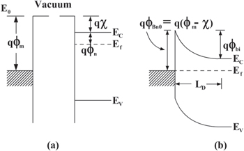
Figure 1. Energy-band diagrams of MSJs. (a) Relative electronic energies of a high work-function metal and an n-type semiconductor in separate systems. The work function of the metal q ϕm is the difference between the Fermi level Ef and vacuum level E0 [5]. (b) Relative electronic energies of the two systems in intimate contact. As the distance between the two systems is decreased, a barrier q ϕBn0 between the interface results, as shown in (b). The band bending in the semiconductor represents the built-in potential, where ϕbi = ϕm − χ − ϕn. From [5] John Wiley & Sons. Copyright © 2007 John Wiley & Sons, Inc. All rights reserved.
Download figure:
Standard image High-resolution imageThe standard ideal description of MSJs assumes that (a) a maximum electric field occurs in the semiconductor, very close to the interface (due to image charge lowering) [13], (b) the only charges involved in the semiconductor are the donor impurities with concentration ND, and (c) the space charge region is confined to a depletion zone, delimited by width WD. Solving the Poisson equation we find

where  s is the dielectric constant of semiconductor, kB is the Boltzmann constant, T is the temperature in Kelvin, V is the applied voltage, and ϕbi is the band bending in the semiconductor, known as the built-in potential. The length of the depletion region decreases with increasing doping concentration, which in general is limited by the solid solubility limit of the particular dopant. Note, however, that advanced techniques such as gas immersion laser doping [14] can overcome this limitation and are an important area of ongoing research.
Image charge lowering plays a role in the electrostatics during electron transport and becomes increasingly important in reduced-dimensional devices. As depicted in figure 2, this lowering is the result of the reduced field at the interface from the electrostatic attraction of a negative charge moving towards it. The resultant image charge lowers the barrier by

where E is the externally applied electric field across the metal/semiconductor interface.

Figure 2. Energy band diagram of Schottky barrier lowering between a metal surface and an n-type semiconductor. Note that the barrier is not at the MSJ, but is located at a distance Xm from the interface. [5] John Wiley & Sons. Copyright © 2007 John Wiley & Sons, Inc. All rights reserved.
Download figure:
Standard image High-resolution imageAlthough this ideal theory is taught in semiconductor physics classes, we know from extensive research that the observed barrier height is rarely the one obtained from this analysis. While larger work-function metals do tend to have larger barrier heights, the dependence is much weaker than expected. The lack of correlation between the barrier height and the work-function is often attributed generically to 'Fermi-level pinning', covering a wide variety of different effects, including inhomogeneities at the junction, surface states at the interface due to either defects or to metal induced states, or chemical bonding at the interface [15]. Many of these models have similar dependencies with temperature and voltage and it is therefore difficult to disentangle the origin of the deviations of the barrier height without additional structural characterization techniques or different experimental conditions for the formation of the SB. Nevertheless, enormous progress in understanding has been achieved, as described in two excellent review articles [15, 16]. This progress originates from three significant advances: (1) the realization of epitaxial MSJs using molecular-beam epitaxy resulting in inhomogeneity-free interfaces, (2) the advent of scanning probe technologies allowing electrical measurements of nano-scale junctions, and (3) the development of powerful computers enabling first-principles ab initio calculations. This knowledge now makes it possible to understand and engineer the SB to a high degree of precision. For simulations and after an eventual optimization of the experimental devices, the Schottky barrier height (SBH) can be considered a parameter obtained from measurements. The mostly widely explored MSJs involve silicon/metallic silicon alloys, known as silicides, because of their wide industrial use in CMOS technology. These investigations have allowed thorough investigations of Si SBMOSFET devices.
Understanding the SB formation in more novel materials is an important subject of current research. An excellent review on the nature of contacts with one- and two-dimensional materials can be found in [17], while more recent reviews focused on two-dimensional materials can be found in [18–20]. Understanding the image charge lowering in bounded geometries [21] and the variation of the SB height in nanowire geometries have been explored by Calahorra et al [22], and measurements of barrier heights on Si nanowires using photoemission have been carried out by Yoon et al [23].
1.2. Current Transport
Electron transport in rectifying MSJs can be broadly grouped into 3 limiting transport mechanisms [5, 24]: (1) transport over the barrier, (2) tunneling through the barrier including direct, thermal- and trap-assisted tunneling, and (3) mechanisms occurring just adjacent to the barrier, such as diffusion and recombination. The overall current is modeled by a combination of these processes. Room temperature transport processes at the SB junctions that are used for transistors are most typically fully described by transport over the barrier via thermionic emission (TE), and direct/thermal assisted tunneling through the barrier [9], which are therefore the focus of this section.
The large majority of treatments of the current transport in SB diodes use semi-classical approximations. For TE and diffusion transport the basic equations can be rigorously derived from the Boltzmann transport equation [25], which provides a complete description of the distribution function. This formalism assumes that the band structure can be included into an effective mass and that the potential due to the applied field is small and does not vary rapidly in space.
The thermionic theory, proposed by Bethe [26] in 1942, describes how carriers with energies larger than q ϕBn or q ϕBp overcome the SB and contribute to electron transport. The total current is the sum of the two current densities that flow from the metal to the semiconductor and from the semiconductor to the metal. The current density is found by integrating over the concentration of electrons with velocities vx in the transport direction and sufficient energy to overcome the barrier. In this classical calculation, the velocity is isotropic and given by a Maxwellian distribution with band structure taken into account via an effective mass m*. The sum of both current contributions for electrons is given by [13, 27–29]

where

Here ϕBn0 denotes the intrinsic barrier height and

is the effective Richardson constant with h the Planck constant and m* the effective mass. In this approximation quantum-mechanical reflections and optical-phonon scattering have been neglected, but detailed research has shown how to include these effects [28, 30] and subsequently how to include them in a modified effective Richardson constant. In silicon, A* = 120 A cm−2 K−2 for electrons and 40 A cm−2 K−2 for holes. Other descriptions of transport over the barrier can include diffusion theory [5], which becomes important for materials with a small density of states. Image-force lowering must also be included, where the resulting barrier height ϕBn0 for electrons from equation (4) is reduced by Δϕ from equation (2) [5]. The effective mass in the prefactor of this equation results in lower thermionic field emission for materials like Ge and GaAs.
Typical treatments of quantum mechanical tunneling in SB devices follow the method first considered by Bardeen [31], originally developed to explain tunneling in superconducting electrodes separated by a thin oxide. It was later extended by Harrison [32] to include regions of varying band structure. This approach solves the Schrödinger equation directly by separating the system into distinct sub-systems with known Hamiltonians and then uses the Fermi golden rule to obtain the transition probability, assumed to be constant in energy. Stratton first applied it to tunneling between two conductors through an insulator, assuming parabolic energy-momentum relations [33], and later to SBs [24]. The main shortcoming of the latter paper was that the pre-exponential terms in the forward and reverse bias resulted in different constants, such that it was unable to obtain zero current at zero bias. This was resolved by the work of Crowell [13], who noticed that due to image charge lowering the barrier occurs not at the metal/semiconductor interface but inside the semiconductor. Therefore, the effective mass in the Richardson constant should always be that of the semiconductor.
Following Crowell, the tunneling current from the semiconductor to the metal (after integration over momentum transverse to the metal/semiconductor interface) is given by [34]

where fs(ξ) and fm(ξ) are respectively the Fermi–Dirac distribution functions of occupied states on the semiconductor side of the junction and unoccupied states on the metal side of the junction, and  is the one-dimensional transmission probability for the barrier with an energy ξ, associated with the component of momentum normal to the metal-semiconductor interface. Note that this equation can also describe TE when
  and the limits of integration extend to the top of the barrier. In this framework, calculating the tunneling current is reduced to calculating the transmission coefficient.
Before discussing how the transmission coefficient can be calculated, we first briefly discuss the Richardson constant A*, which appears in both the tunneling and the TE equations. In the ideal theory A* is defined by equation (5), but the effective mass used in this equation can be different for direct tunneling versus thermally assisted tunneling and TE [13, 25]. Nevertheless, this work assumes that the effective mass should be that of the semiconductor and independent of the metal and that there is no interfacial oxide layer between the metal and the semiconductor. Research by Toyama has shown, however, that the Richardson constant varies with film thickness [35, 36]. Work exploring tunneling of metal-insulator-semiconductor junctions showed that the effective mass of each region needed to be included in order to correctly match boundary conditions [37, 38]. Variations of the Richardson constant from the ideal value are thus often attributed to the presence of a tunnel barrier at the MSJ and the resulting impact due to the additional prefactor from this mismatch of effective mass. More recently, the effective mass of the metal was used to obtain a value intermediate between that of the metal and that of the semiconductor, and was used to explain TE transport in SB SiC diodes [39].
The transmission coefficient T(ξ) has been the target of many different approximations. The most extensively used technique is the Wentzel–Kramers–Brillouin (WKB) approximation, which assumes that the amplitude of the wavefunction varies slowly compared to the phase so that, as in the classical case, the total energy is greater than the potential energy [40–42]. The Gundlach method [43] assumes that the potential barrier is linear, and transforms the Schrödinger equation into Airy functions. The transfer matrix method approximates the barrier in the transport direction as piecewise linear functions and determines the transmission coefficient for each one. Finally, the wavelet methodology approximates the wavefunction by a wavelet [44, 45].
We briefly recall the WKB approximation for determining the transmission coefficient [40–42]:

where x1 and x2 are the classical turning points, ξ ≤ V(x) and equation (7) is real. This approximation has been extensively explored by Padovani and Stratton [24] for barriers of arbitrary shape. Most often, however, it is approximated as triangular, with V(x) = q ϕBn0 − qEx. This results in the analytical solution

which leads to Fowler-Nordheim type equations.
As devices are scaled down, three-dimensional calculations become inaccurate. Other formalisms that can be employed include Wigner functions, the non-equilibrium Green's functions (NEGF)—Landauer method and/or combining these with ab initio calculations. The Wigner distribution function method [46] has typically been used to explore transport in systems far from equilibrium, most notably resonant tunneling diodes [47], where the non-stationary description is important. It models the system using a density operator (the Wigner function) whose time evolution is given by the Liouville-von Neumann equation. Solutions can be obtained using either finite difference or Monte Carlo methods. This technique has also successfully been applied to explore quantum transport in ultra-scaled MOSFETs [48].
A large majority of the models that are used to model transport through the SBs in SBMOSFETs are based on the semi-classical TE and tunneling methods because the quantum methods consume large computing resources for just the calculation of transport at the SB. Quantum techniques that describe transport in SBMOSFETs typically use the SB height as a boundary condition, grouping the different types of transport into a unified treatment [49, 50].
1.3. Silicon and germanium SBMOSFETs
During the past 25 years, research has shown that Si SBMOSFETs are intrinsically lower cost, more energy efficient and inherently more scalable than conventional doped source/drain MOSFETs [7–9]. As a result of the many obstacles in realizing this technology, however, there has been little industrial exploitation. We briefly review their fabrication and advantages as they serve as a basis for all the SB transistors considered in this review.
SBMOSFETs as depicted in figure 3(a), are realized by depositing a metallic layer onto the semiconductor source and drain contact regions, typically with a self-aligned process. To ensure reproducible, void-free and geometrically well-defined metal/silicon interface regions, a post-deposition anneal (PDA) step is carried out. In silicon the metallic region formed by the PDA typically results in a metallic alloy, known as a silicide [51]. These materials have been widely used in conventional doped source/drain FETs (DSDFETs) to realize ohmic contacts at the doped source and drain regions, as well as for doped poly-Si gate electrodes. The formation of many metal silicides is a result of the diffusion of the metallic atoms into the silicon. For SB transistors this leads to an overlap of the source/drain regions with the gate and additional control over the band bending near the interface. MSJs involving low-doped silicon result in Fermi-level pinning closer to the valence band edge, resulting in a low SB height for holes. Rare-earth silicides such as those involving yttrium, erbium, holmium, dysprosium and gadolinium [52] form low n-type Schottky barriers to silicon. By comparison, for Ge, where the metallic compounds are known as metal germanides [53], there is generally a lower phase stability compared to silicides.

Figure 3. (a) High-resolution TEM of a 22 nm p-type SBMOSFET. (b) A Schottky barrier exists along the perimeter of the source (and drain) electrodes, where there is contact to the silicon substrate. This barrier presents an impedance to the flow of current in the device that is not present in a conventional doped source/drain MOSFET. The electric field  at the SB, indicated by the arrow is normal to the metallic surface and therefore has a strong lateral component, especially near the source. In contrast, the electric field near the source in a conventional device (c) is nearly vertical.© [2006] IEEE. Reprinted, with permission, from [7].
Download figure:
Standard image High-resolution imageDepending on the SB height of the junctions, two distinct operating regimes are differentiated: (a) unipolar SBMOSFET with small barrier height or near-ohmic contacts for electrons or holes and (b) ambipolar SBMOSFET with a substantial barrier height for both electrons and holes. An ideal SBMOSFET for high performance computing corresponds to type (a), with the SB at the source playing a significant role in preventing the 'off' state leakage current between the source and the channel [7]. In the on state the SBs would become nearly or even completely transparent and the device would operate as a conventional doped source/drain FET (DSDFET). In the ideal case then, the difference in transport would be predominantly found in the sub-threshold region. For low power analog electronics, case (b), ambipolar SBMOSFETs can be employed, as will be discussed in the section on ubiquitous computing. Figure 4 shows a schematic band diagram and transfer characteristics of a Si SBMOSFET device. Figure 4(a) is biased as a p-type transistor in the on state, where the band bending is inverted so that not only TE over the barrier occurs but also direct and thermal assisted tunneling processes. These are the same processes described for MSJs in section 1.2. An example of the characteristics of a pSBMOSFET is shown in the device in figure 4(b) with a Subthreshold Swing SS of 92 mV Decade–1. Understanding the current transport mechanisms in the sub-threshold and other regimes of operation is an important part of the literature. Note that the effective barrier to transport in the sub-threshold regime includes not only the SB height, but also the height of the bands that rises above it. In this region, transport occurs by TE and the current is very small. Nevertheless, the changing effective barrier height to carriers, due to changes in gate potential, causes large changes in the sub-threshold current in the channel. The threshold voltage in bulk SB devices can thus be defined as the Vg value corresponding to the flat-band voltage [54].
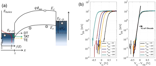
Figure 4. (a) Schematic band diagram of a p-type SBMOSFET in the 'on' state with three possible types of transport indicated (direct tunneling, DT, thermal assisted tunneling, TAT, and TE). (b) Room-temperature characteristics of an experimental PtSi-based SBMOSFET on FDSOI at Vd = 100 μA. The transistor was fabricated using standard CMOS technologies [55, 56] with a buried oxide layer (BOX) of 145 nm and a slightly n-doped channel (800 nm wide/60 nm long). The silicon substrate can be used as a back-gate, in addition to the top gate. (Left) Source/drain current Ids vs top-gate voltage for various values of the applied back gate voltage Vbg. (Right) Scaling of Ids vs Vg−VTh for various values of Vbg. The solid line shows the SS.
Download figure:
Standard image High-resolution imageIdeally, on-state device performance is equivalent to that of DSDFETs. In practice, however, this will occur only when the SB is completely transparent, which is challenging to achieve. Nevertheless, linear or ohmic contacts can be realised by strong or even degenerate doping of the semiconductor, where the SBH to the valence or conduction band edges can be reduced to 0.1 eV. Moreover, for doped Si and Ge semiconductors a special situation can occur during the PDA when the phenomenon of dopant segregation takes place. This has been observed experimentally through ion SIMS profiles and further described theoretically with DFT calculations by Kinoshita et al [57]. Typical dopant impurities for Si and Ge, like P, As, Sb and B, show a low or even zero solubility in many metal silicides and germanides [58]. Consequently, during the metal-silicide/-germanide growth, the impurity atoms initially residing in the transformed semiconductor region are dissolved and displaced by diffusion and finally accumulate in the semiconductor adjacent to the MSJ. Measurements show that the dopant atoms are not built into the semiconductor lattice because of the low silicide formation temperatures. Instead, they tend to reside as interstitials, influencing the band alignment at the Schottky junction. Experiments demonstrated that B and As dopants in CoSi2/Si junctions [57] and B, P and As dopants in Nix Si1−x /Si films [59] are the most efficient for dopant seggregation.
The SB at the source/drain will thus influence the flow of current and the distribution of charges and depend on the device materials, the voltages, temperature of operation and other factors such as interface states, barrier inhomogeneities [60], etc. The device physics of the SBMOSFET can be quite complex. We now address the more subtle differences between SBMOSFSETs and DSDFETs with a focus on the advantages of SBMOSFETs.
1.3.1. Charge transport near the Schottky barrier
The metallic source/drain electrodes constrain the electric field to be normal to their surfaces and will be determined almost exclusively by the shape of the metallic electrodes, as shown in the simulations in figure 5. This contrasts conventional DSDFETs, where, except in specific circumstances, such as near the drain under high drain voltage, the field near the source is largely vertical. It is independent of the details of the source/drain regions, as shown schematically in figure 3(c) and in the lateral direction by the simulations in figure 5. Carrier emission from the source is simply from one type of silicon to another and there is no abrupt change in velocity as charge carriers transit from source to channel.
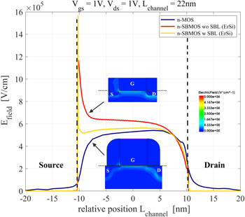
Figure 5. Comparison of the electric field underneath the silicon oxide of n-type SBMOSFET versus classical n-type MOSFET (coordinates origin set to the center of the device). The simulations were performed for the follwing device charactersitics: Vd = 1 V, Vg = 1 V, T = 300 K, Lchannel = 22 nm. The electric field for the SBMOSFET is one order of magnitude greaterthan for the MOSFET. The effect of Schottky barrier lowering strengthens this effect. Note that ErSi was introduced with a Schottky barrier height of 0.27 eV and a nonlocal tunneling model was used for the n-type barrier.
Download figure:
Standard image High-resolution imageMultiple authors have explored experimentally and via two-dimensional (2D) technology computed aided design (TCAD) simulations the effects of a metallic source/drain on device performance. A review from 2006 describes earlier devices [7], while Valentin [61–63], Pearman [64, 65], Raskin [66] and Du [67] have documented the differences in transconductance (gm), gate capacitance (Cgg) and unity current gain frequency (fT) between SBMOSFETs and conventional DSDFETs. All of these investigations show that despite reductions in gm, fT is higher for SBMOSFETs compared to DSDFETs because of significant reductions in Cgg. The root cause of the reductions in Cgg with finite SB height at the source/drain junctions remains unclear, but we see two possibilities. The first is that the SB limits transport in the channel resulting in less charge and therefore less sensitivity in the channel region to changes in gate voltage, as explored by Valentin [61] and Pearman [64]. The second one is that strong lateral electric fields near the source result in 'hot' charge carriers—carriers not in thermal equilibrium with the lattice—transiting the channel at a depth somewhat beneath the gate oxide. These carriers are likely 'hot', due to large initial velocities when emitted from the metallic source electrode, where Fermi velocities can be 10–20 times the saturation velocity of carriers in silicon. A qualitative comparison of the inversion layers—not based on simulation but rather educated approximation—is shown in figure 6. Within the Thomas–Fermi approximation, carriers leaving the source will travel approximately the Debye length before their velocity adjusts to that of the semiconductor [5]. Such effects have been especially observed to result in a strong injection of charges from the source into the gate in asymmetric transistors with a single source SB, such as in [68]. This effect should become more important as device dimensiond approach the Debye length, (20 nm at a doping of 1 × 1017 cm−3[5]). Its existence could explain, at least in part, the observed decrease in Cgg.
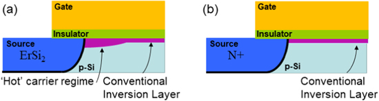
Figure 6. Schematic depiction of carrier injection from the source into the channel region for: (a) an SBMOSFET and (b) a conventional DSDFET. In the case of (a), large lateral electric fields near the source are postulated to produce hot carriers, that is, carriers not in thermal equilibrium with the silicon lattice, a phenomena that is not observed in (b), which features a conventional inversion layer in thermal equilibrium with the lattice at the source-end of the device.
Download figure:
Standard image High-resolution imageA series of papers by Shih, Luo and co-authors [69–73] have examined, both via 2D TCAD simulation and experiment, the effects of metallic source and drain electrodes on the performance of both floating gate and charge trapping non-volatile memory cells. Their results show how charge carriers near the source attain velocities large enough to enable charge trapping in oxide-nitride-oxide (ONO) structures, something that is not observed in conventional DSDFETs, in accordance with the schematic depiction in figure 6. Further, programming efficiencies are observed to be several orders of magnitude larger for SBMOSFETs, which can be explained by large velocities near the source. Simulations of injected charge in ONO films show the lateral extent of the charge distribution to be around 20 nm, about 3 × smaller than for conventional DSDFETs, and in agreement with the order of magnitude of the Debye length.
The effects of these source-side hot-carriers on long-term device degradation and reliability has received little attention in the literature and is a field of study that deserves significant attention.
1.3.2. Lower parasitics and off current
There are two parasitics that can be significantly different in SBMOSFET devices: the parasitic series resistance, the parasitic bipolar gain. The parasitic series resistance, defined as unwanted resistance external to the channel of the transistor, is greatly reduced in an SBMOSFET compared to a conventional DSDFET. The MSJ resistance, which is the largest component in a DSDFET, is now technically part of the channel in an SBMOSFET and is therefore no longer parasitic. While this may seem a mere exercise in semantics, there are important differences. In DSDFETs, the resistance associated with the SB, RSB is generally a fixed, constant number and depends only on the SB height and doping density on the semiconductor side. Often, a mid-gap SB system is used (for both p and n-FETs), with a high doping density.
As we saw from our discussion above, RSB for an SBMOSFET strongly depends on the gate voltage. Typically a metal with a low SB to the conduction band of the semiconductor is used for n-type devices and a metal with a low SB to the valence band is used for p-type devices, with the exception of RFETs, which require mid-gap SB heights. The overall channel resistance of an SBMOSFET, including the Schottky junctions on either end, is therefore a strong function of the gate voltage. The sheet resistance of the metal, Rsh, which is 1–2 orders of magnitude smaller than that of doped silicon, is still present, depicted in figure 7. There is also the very small metal-to-metal contact resistance (Rcon) to the plugs, which connect to upper metal layers. The parasitic resistance in an SBMOSFET is therefore an almost negligible fraction of the total resistance (typically ∼1% or less [7]). For a conventional DSDFET the parasitic resistance can be much larger, as high as 50% in highly scaled devices.

Figure 7. Parasitics in SBMOSFETs. For SBMOSFETs RSB is technically part of the channel and is therefore not parasitic. The relatively small sheet resistance (Rsh) of the metallic source (and drain), along with the very small metal-to-metal contact resistances (Rcon) of the plugs from the upper layers of metal make up the total parasitic resistance for the SBMOSFET. The intrinsic parasitic bipolar transistor is also shown.
Download figure:
Standard image High-resolution imageAn n-type DSDFET typically has heavily doped n-type source/drain regions and an oppositely doped (p-type) body region. As a result, there is an unavoidable parasitic NPN bipolar transistor. Under normal operating conditions this NPN is dormant, as the base-emitter junction is not forward biased because the source and body potentials are usually tied together or, in some cases, reverse biased. However, the body can become forward biased with respect to the source if, for example, the p-type body is filled with holes resulting from either impact ionization in the inversion layer or from an ion-strike. The NPN can then become activated and will amplify the original hole current into a much larger electron current. Bipolar amplification gains of around ∼200 × are typical for silicon NPN devices. Worse, this mechanism can, under the right conditions, become self-sustaining and uncontrolled by the gate electrode, usually resulting in the destruction of the device and the surrounding circuitry. This positive feedback loop can occur within single transistors or in CMOS circuits with complementary n- and p-type devices. Modern device designs such as fully depleted silicon on insulator, FDSOI, Tri-Gate FETs, FinFETs, and GAAFETs attempt to mitigate this problem by operating at low supply voltages to minimize impact ionization and also by minimizing the volume of the body region to limit charge collection during an ion-strike. SBMOSFETs, however, have a key advantage in this respect: the gain of the NPN device is much less than unity, and therefore the positive feedback loop mentioned previously cannot exist. This is due to differences between the physics of current transport across a Schottky junction (thermal emission) vs a p–n junction (drift-diffusion). As a result, SBMOSFETs are inherently immune to all parasitic bipolar action. This is true regardless of device profile, doping profiles, ionization radiation intensity, temperature, device layout, operating voltage, etc. Device design is thus liberated from having to consider unwanted bipolar gain, providing a real advantage especially in some cases, for example in power devices.
Minimizing the off-state leakage between source and drain in DSDFETs is a major challenge for highly scaled devices where direct source-to-drain tunneling currents can occur. The presence of a finite SB at the source/channel interface therefore provides SBMOSFETs with a built-in advantage. Modern device designs such as the tri-gate FET, FinFETs and gate-all-around FETs (GAAFETs) are all attempts to exert greater gate control over the channel in order to reduce off-state leakage while keeping on-state drive current large.
The leakage currents in a conventional DSDFET are controlled by creating electrostatic barriers in the channel, denoted as ϕes, by introducing dopants of the appropriate type, concentration and location into the substrate, and/or gate material engineering. These techniques work equally well in an SBMOSFET and serve to augment the existing SB, ϕSB, in order to create a larger total barrier (ϕtot) and lower the leakage current. The presence of a finite ϕSB allows for a measure of flexibility in device design. Specifically, ϕes can be reduced via channel doping and/or gate material engineering, to keep the leakage current constant compared to the zero-ϕSB case. Simulations have shown that the channel doping for a 25 nm SBMOSFET can be reduced by as much as 1–2 orders of magnitude [7]. Reductions in channel doping may also lead to beneficial reductions in gate and junction capacitance, due to the wider extension of depletion regions. Of course, the presence of a SB will also impede the flow of current in the on state. The net effects of the SB on both the drive and leakage currents will depend on the details of the device architecture: SB height, source and drain position and profile, channel dopants, channel length, etc.
As devices approach the sub-10 nm regime, direct source-to-drain tunneling becomes important in MOSFETs. Simulations by Cho et al used NEGF simulations to compare sub-10 nm SB and double-gate MOSFETs and showed that methods such as source/drain underlap and optimization of the body thickness can suppress direct source-to-drain tunneling in both devices, but that the double-gate MOSFETs show higher performance due to higher drive currents [8]. The caveat of this work, however, is that the SB was assumed to be 0.1 eV, and image charge lowering was not considered. Semiclassical simulations that do take this into account suggest that at nanoscale sizes the image charge lowering can reduce the barrier sufficiently to make it transparent [9].
1.3.3. Improved Manufacturability
If the metallic source/drain regions of an SBMOSFET are silicides, as is almost always the case in Si devices, there are several manufacturability advantages compared to a conventional DSDFET (figure 8). Most important are the simplicity and lower energy associated with the silicide formation. Metal deposition, anneal and unreacted-metal strip are done at much lower processing temperatures compared to doping, and are high-throughput and high-yield steps. Silicides for both p and n-type devices, for example PtSi and ErSi2 respectively, are typically formed at 450 °C, cause no damage to the lattice, and result in low-resistance films that have atomically abrupt interfaces to the silicon substrate. The final lateral and vertical extent of the silicide film is determined by the thickness of the original metal layer, which, once reacted to completion, is invariant with additional annealing, thus providing a wide process margin. The contact resistance of these silicides to metal 'plugs' from upper metal layers is also very small, as expected for metal-to-metal contacts. Overall the SBMOSFET will have fewer processing steps and also consume less energy due to removal of the doping steps. Therefore, it remains a very interesting device for industrial use, especially for applications seeking to reduce energy consumption and process complexity.

Figure 8. An illustration of the manufacturability advantages of the SBMOSFET over conventional DSDFETs.
Download figure:
Standard image High-resolution image2. Schottky barrier transistors in high performance computing applications
A large part of the semiconductor industry focuses on realizing the fastest and smallest transistors for intensive computing applications such as data centers, scientific calculations and artificial intelligence. Conventional techniques to improve MOSFET performance are (1) reducing the channel length (and simultaneously scaling the other parameters to limit short channel effects); (2) thinning the transistor's body (as in FDSOI devices) or wrapping the gate all-around the channel (as in trigate or GAA transistors) to improve electrostatic control over the channel potential; and (3) increasing the channel carrier mobility using a combination of materials and strain engineering.
Shrinking transistor dimensions using a top-down approach becomes increasingly difficult at nanoscale sizes. For this reason, there is great interest in bottom-up fabrication strategies, and in particular synthesizing nanoscale building blocks such as nanowires, nanotubes, graphene and transition metal dichalcogenides for use as starting materials. Transistors made from these nanomaterials can be considered as TFTs, but historically, these two communities have had limited interactions. A recent article makes important inroads into developing benchmarks and performance metrics [74]. An overview of nanomaterials in transistor geometries can be found in [75], the use of 2D materials for future integrated circuits is discussed in [76], and [77] provides a recent overview of digital electronics using carbon nanotubes. Excellent reviews on the state of the art of nanowire electronics and bottom-up silicon nanowires can be found in [78] and [79, 80] respectively.
There has become a fine line between technologies meant to target high performance computing applications and those that can be used for ubiquitous electronics, discussed in section 3 of this article, as what might be a detriment in one may serve as an advantage in the other. In this section, we consider devices realized in 1D and 2D materials and focus on how the SB can be problematic for high performance devices. This leads to section 3, ubiquitous electronics, where the focus is on devices that can take advantage of the SB.
2.1. 2D materials
2D materials are an ultimate solution to thinning the transistor body to improve electrostatics. The atomic thickness may enable very small gate length 2D FETs, thus paving the way for gate length scaling into the nanometer and even sub-nanometer regime [76, 81]. The significant ongoing research and development effort has resulted in the technology being identified by the international roadmap for devices and systems (IRDS) as a potential candidate for devices beyond CMOS [2]. Nevertheless, a large contact resistance is observed in 2D devices, typically preventing experimental realizations that are competitive with contemporary Si or even Carbon NanoTube CNT technology.
These materials exist in a large variety of classes including metallic, semiconducting, insulating, and recently even magnetic and superconducting. The schematic comparison of 2D and bulk materials in figure 9 [81] shows how the surfaces of 2D materials are free from dangling bonds, consistent with physical properties at the monolayer regime [82–84]. A dominant critical issue is therefore the interface engineering and especially the optimization of the contacts. Several proposed solutions include inserting a buffer layer between semiconductor and metal, realizing van der Waals (VdW) contacts, edge contacts, novel doping and surface engineering. These techniques have been described in an excellent recent review [20]. Nevertheless, SBs can easily dominate the transport and many 2D semiconducting transistors are essentially small-scale SBFETs [85].
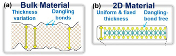
Figure 9. Schematic representation of (a) a very thin bulk material and (b) a 2D material with atomic thickness levels. © [2015] IEEE. Reprinted, with permission, from [81].
Download figure:
Standard image High-resolution imageAlthough the first exfoliated 2D semiconductor was reported in 1986 [86], it was the demonstration of the electric field-effect in single layer graphene, exhibiting unprecedented carrier mobilities and ballistic transport at room temperature [87], that sparked the recent intensive research effort. Graphene, however, has a zero band gap and is not suitable for logic applications, although it may find use in radio frequency applications [88]. Numerous 2D materials have been explored in this context for the past 10 years and are the subject of ongoing research to develop potential electronic applications [89, 90]. Of particular importance are single-layer 2D FET devices based on the transition metal dichalcogenide (TMDs) family, which have a general formula MX2, where M is a transition metal (e.g. Mo, W) and X is a chalcogen atom (eg. S, Se, Te) [91]. Mo and W-based TMDs are semiconducting with a thickness-dependent band gap that transitions from indirect (bulk) to direct (up to a few-monolayers) [92]. Cao et al rigorously analyzed the performance and scalability of 2D semiconductors, especially MoS2, through dissipative quantum transport simulations for sub-10 nm technology nodes [81]. Figure 10 clearly demonstrates that MoS2 transistors outperform Si devices in terms of (a) evaluated SS and (b) drain induced barrier lowering (DIBL). In (c), calculated Ion for devices with different numbers of layers of MoS2 and Si are compared for high performance and low standby power technologies. It is observed that MoS2 devices show higher Ion compared to Si devices because of the poor electrostatics in the latter. More than 3 layers of MoS2 must be avoided for sub-10 nm nodes, however, because of worsening electrostatics. Experimental MoS2 FETs have indeed shown superior immunity to short-channel effects [93], and also high saturation velocity (2.8× 106 cm s−1) in few-layer devices [94]. Nevertheless, the main problem remains the high source/drain contact resistance. Shen et al have recently reported breakthrough results of ultra-low contact resistance using Bi contacts to MoS2 transistors, and proposed that Bi-TMD technology could potentially meet the IRDS targets for logic transistors [95]. Nevertheless the thermal stability of this solution may prevent its large scale implementation.
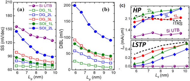
Figure 10. A comparison of (a) SS, (b) DIBL, and (c) on-current vs gate length for ultra thin body Si, and one to three layer (L) MoS2 FETs that are double-gated or semiconductor-on-insulator (SOI) structures. HP and LSTP stand for high performance and low STandby power technologies. © [2015] IEEE. Reprinted, with permission, from [81].
Download figure:
Standard image High-resolution imageIt has been more difficult to realize p-type TMD FETs due to strong Fermi-level pinning at the semiconductor interface with most metals, which also results in large contact resistances [96]. Li et al fabricated p-FETs based on few-layer black phosphorus (BP) that demonstrated reliable performance and ambipolar behavior [97]. Realization of transistors in ambipolar materials such as WSe2 and WS [98] have also been explored. To date their device performance for high performance computing has not been assessed as well as the MoS2 devices.
In order to improve the performance of existing FET technology based on 2D materials, different device architectures are also being investigated. These include devices based on vertical and lateral heterostructures of 2D materials. 2D–2D heterostructures are known to form either Schottky contacts or PN junctions, depending on the type of material used. Graphene is generally used as the contact material, while semiconducting 2D materials are used as the channel or junction materials, and hBN is used as the gate dielectric [99]. Heterojuction FETs based on heterostructures of 2D/3D materials are also being investigated. Here, 2D materials have an edge over conventional channel materials such as Si for the fabrication of ultimately scaled heterojunction FETs, as field-effect modulation of the current transport through the heterojunction provides a unique opportunity to realize band-to-band tunneling devices.
Perhaps the greatest promise for 2D materials for high performance computing is the possibility to design novel devices, and ultimately architectures based on stacking, that is not possible in conventional silicon technologies. Two recent review articles have detailed this in greater depth [100, 101]. In this way, the disadvantage of the source/drain contact resistance is offet by an advantage not possible in conventional semiconductor technologies.
2.2. Carbon Nanotubes
Single-walled carbon nanotubes (SWNTs) and nanowires have been considered as potential building blocks for future microelectronic devices because of their very small diameters and the excellent properties exhibited by single-transistor devices. Like 2D materials, the connection between nanotube and metallic contacts results in a SB, but solutions are now available to render the barrier negligible in the on-state. Simulations predict impressive 5-fold [102] to 9-fold [103] improvements in the energy-delay product (EDP) (notably coming from lower-bias operation) in comparison to Si or Si/SiGe FinFETs. The two main difficulties have been synthesizing only semiconducting SWNTs and doping the nanotubes, but some laboratories have now met the criteria for ultra large scale integration [77]. In order to do justice to this very large body of work, we first provide an overview of the advantages and disadvantages of this technology. We then focus on the role of the SB between the nanotube and the metallic contacts.
SWNTs are hollow cylinders made of sp2-bonded carbon atoms, with a diameter in the 0.7–3 nm range. Their structure, properties and applications have been thoroughly reviewed [104–106], as well as their specific electronic and transport properties [107, 108]. Depending on their chirality (diameter and helicity), they can have a metallic or semiconducting character. In the latter case, their direct band gap scales as ∼0.8/d (with d the diameter in nm) so that typical diameters (1–1.4 nm) yield sizable band gaps (0.6–0.8 eV).
The most important assets of SWNTs in the context of carbon nanotube FETs (CNTFETs) are: (i) their atomic structure is free of dangling bounds and rugosity (which notably makes them compatible with high-κ gate dielectrics without mobility degradation [109–111]); (ii) their band structure is symmetric for holes and electrons (resulting in similar m⋆ for both types of charge carriers); (iii) their capacitance is low [112], which is particularly advantageous at high-frequency [113, 114]; (iv) they have exceptionally high carrier mobility for both electrons and holes; (v) they can withstand extremely high current densities (>0.5 mA μm–2 for arrays) [2]; and (vi) charge back-scattering processes associated to defects are not efficient; (vii) at low electric field the electron (and hole) mean free path associated with acoustic phonons is as high as 300–500nm. It is reduced to ∼20 nm at high electric field due to optical phonons [108, 115, 116].
Transport in SWNTs is mostly ballistic at low bias in long-channel devices (<300 nm) and at all biases in aggressively scaled devices (<20 nm). The mobility in long SWNTs (corresponding to low electric field) scales as d2/T [117], and at RT it has been estimated to be >105 cm2 V−1 s−1 for large diameter nanotubes [115]. The highest experimentally measured value, however, is μ = 79 000 cm2 V−1 s−1 for an ultra-long SWNT (L > 300 μm) [118] but values in the 2500–20 000 cm2 V−1 s−1 range are more typical.
This technology also has some disadvantages. The main one is the difficulty in synthesizing uniquely semiconducting nanotubes. In addition, substitutional doping, which is one of the great strengths of silicon technologies, is not possible in carbon nanotubes. Alternative chemical and electrostatic doping strategies exist but are often unstable (such as potassium or molecular doping) and/or poorly scalable (such as multiple gates). It also remains extremely difficult to control the selective placement of SWNTs. To obtain high enough drive currents, optimized CNTFETs need to be composed of several parallel nanotubes with an optimized CNT–CNT pitch (5 nm) [75, 102], small enough to allow high current densities but not too small to ensure that the advantage of 1D electrostatics can be maintained. Research therefore focuses either on demonstrating devices and circuits using FETs made up of arrays of CNTs, or transistors with an individual nanotube, to explore device properties and scaling. Arrays typically exhibit a degraded SS and leakage current [119], due to the presence of metallic nanotubes.
Individual SWNTs were integrated as channels in FETs as early as 1998 [120, 121]. In these devices and in most of the following ones, metallic source and drain electrodes directly connect the undoped nanotube channel so that they operate as Schottky-barrier FETs [122]. Such SBMOSFET operation is notably central to understand their (lateral and vertical) scaling behavior [109, 123–125]. The change in band gap with diameter renders large diameters subject to ambipolar leakage currents, and very small diameters susceptible to large contact resistance. The ideal diameter has been predicted to be ∼1.7 nm [102]. It is important to note that n- and p-type CNFETs operating as conventional MOSFETs (i.e. not as SBMOSFETs) were also fabricated by doping sections of the nanotube close to the metal source and drain electrodes. This resulted in improved performance but, as mentioned, the unstable chemical doping or poorly scalable multi-gate designs used strongly limit their applications when compared with simpler, more scalable self-aligned gate SBMOSFET designs [126]. Recent work has demonstrated a new electrostatic doping strategy to realize excellent control over the p-type and n-type CNTFETs using non-stoichiometric oxides [127].
A crucial difference between conventional metal/semiconductor Schottky contacts and nanotube/metal interfaces is the limited effect of Fermi-level pinning in the latter case. As a result, the SB heights in both p- and n-type nanotube SBMOSFETs were shown to principally depend on the metal work function and on the nanotube diameter (through its impact on the band gap), as shown in figure 11. High work-function metals (e.g. Au, Pd [128]) typically result in good p-type FETs, while low work-function metals (Sc [129], Y [130]) allow good n-type FETs. Interestingly, mid-gap alignment (i.e. high SB height for both electrons and holes) results in low drive currents for bulk-silicon SBMOSFETs, but on the contrary, leads to efficient ambipolar SBMOSFETs with carbon nanotubes [131]. Indeed in SWNTs, band bending occurs at the nm scale and the low m⋆ favors tunneling through high (yet thin) barriers. Note that ambipolar nanotube SBMOSFETs were shown to be important in carbon nanotube optoelectronics, as reviewed in [132, 133].

Figure 11. ION and Schottky barrier height of carbon nanotube SBFETs as a function of nanotube diameter for Pd, Ti, and Al metal contacts. Devices are fabricated on 10 nm SiO2, with channel length of 300 nm and Vds = −0.5 V. Reprinted with permission from [134]. Copyright (2005) American Chemical Society.
Download figure:
Standard image High-resolution imageAnother important observation is the significantly different device performance obtained with metals of rather similar work function. In particular, palladium was shown to be the ideal metal for p-type CNTFET, which cannot be accounted for by its work function alone. This led to a vast number of computational studies addressing the details of the metal/nanotube interface and the impact of weak versus strong interactions on the contact resistance (see notably [135] and references therein). In particular, the contact length Lc (the length of the nanotube section embedded below the source and drain metal contacts), which was initially mostly neglected became a central element in determining the ultimate performance of aggressively scaled devices [136, 137]. Weakly interacting metals (such as palladium) usually give the best performance when Lc is kept long enough (typically above 50–100 nm). But for short contacts, the contact resistance Rc scales as  for most metals (Au, Pt, Pd).
Aggressively scaling the channel length only makes sense if Lc is also drastically reduced, which is why the details of the Rc(Lc) scaling are a central issue in the field. Figure 12 from [135] and [138] summarizes simulations and experiments, and highlights a key element going forward: metals with the lowest Rc at long Lc (notably Pd) may not be those with the best scaling trends. Conversely, Rh, which is not particularly remarkable for Lc = 100 nm, becomes a promising choice for Lc = 20 nm [138]. The current state of the art in terms of scaled contact length consists of either: (i) end-bonded molybdenum carbide contacts that allow high performance (2Rc < 36 kΩ/nanotube) down to Lc = 9 nm. Contrary to Pd and Rh contacts, the nanotube section below the annealed molybdenum metal is destroyed and replaced by a Mo2C carbide, or (ii) more conventional Pd contacts with Lc = 10 nm, which do not require a high temperature annealing step but also yield 2 · Rc = 36 kΩ/nanotube as median value (and even 2 · Rc = 13 kΩ/nanotube for the best device) [139].

Figure 12. Dependence of the contact resistance Rc on the contact length Lc in carbon nanotube SBFETs. (a) Simulations from Fediai et al [135]. (b) Experiments from Franklin et al [138]. Reprinted with permission from [138]. Copyright (2014) American Chemical Society.
Download figure:
Standard image High-resolution imageContact type and contact length optimization is clearly a key aspect for CNT-SBMOSFET improvement. However, the channel length scaling and the choice of the device topology (in particular of the gate stack) are equally important issues. Channel length scaling studies started as early as 2004 with Lch lower than 50 nm [126] and it was later shown that CNT SBMOSFETs with Lch = 15 nm do not suffer from short-channel effects. High performance CNTFETs with channel length below 10 nm [140, 141], even down to 5 nm, were then achieved [142]. In terms of geometry, a large majority of the experimental studies used planar back-gate or top-gate designs. Due to the cylindrical nature of SWNTs, it was naturally considered that a gate-all-around geometry would be ideal from an electrostatic point of view and this geometry was routinely used in calculations [124, 125, 143] In addition, its high symmetry makes the simulation less demanding. Such gate-all-around designs were successfully realized experimentally [144–146]. The cylindrical geometry efficiently shields the channel from parasitic charges, although it is not clear yet whether it actually leads to the best performance. Not only is it much more difficult to engineer, but recent studies have also shown that higher clock frequencies can be obtained with simpler geometries, as exemplified in figure 13 [147, 148], due to reduced parasitics.

Figure 13. Schematic of different CNTFET geometries (a)–(c) and total energy versus frequency of a simulated 32-bit processor showing the Energy Delay Product EDP trade-off curves for back-gate, top-gate, and GAA CNFETs. The back-gate technology was subsequently used to realize a RISC-V microprocessor [149]. © [2019] IEEE. Reprinted, with permission, from [147].
Download figure:
Standard image High-resolution imageAlthough the material characteristics of carbon nanotubes were recognized as promising when they were discovered in 1991 [150], it took 20 years before their use was demonstrated in significantly complex circuits [151]. The research described in this section focused on aligned transistors, the channel of which is either an individual CNT or a large number of parallel CNTs with a channel length much shorter than the CNT length. Another class of nanotube-based devices are CNT-TFTs, for which the channel is a dense array of randomly oriented CNTs with a channel length either longer or shorter than the average CNT length. CNT-TFTS were initially considered for applications that required low to moderate performances (in particular for flexible electronics or flexible displays), because either the density of CNTs was not high or because the channel dimensions were micron size, resulting in relatively small mobilities. These types of CNT TFTs are briefly discussed in section 3.4. More recent research has shown how non-aligned arrays of CNT transistors can be used to realize high speed logic (2 GHz) using high-purity solution processing [152] and how high-performance devices are compatible with fabrication in commercial silicon manufacturing facilities [153]. In the latter reference, simulations showed that the impact of non-aligned TFTs, as compared to aligned arrays, is less than 20% when channel lengths are smaller than 500 nm, and the density of tubes is below 56 tubes/micron. We thus see that many of the problems in realizing CNT devices, such as the purity and positioning, have solutions, and we can expect to see demonstrations of high-performing complex circuits of CNTs in the coming years [154], with the potential to move CMOS beyond Si [149, 155].
2.3. Nanowire transistors
Compared to the CNTs described in the last section, semiconductor nanowires are not closed, allowing the possibility to form bonds with a surrounding medium, for instance with a dielectric material. By varying the nanowire diameter, the electronic structure can be tuned from that of the bulk to one exhibiting quantum confinement, occuring when the diameter is comparable to or smaller than the Fermi wavelength of the semiconductor material. In addition to the possibility of exploiting the one-dimensional density of states, nanowires allow for monolithically combining different materials, which is the relevant for MSJs, both in longitudinal and radial coordinates. Here we focus only on how this type of transistor can be used for SBMOSFET devices.
Semiconductor nanowires are highly promising for implementing diverse types of emerging electronic and optoelectronic devices making efficient use of Schottky junctions. Distinctly different from bulk and thin films, this one-dimensional structure allows for an enhanced relaxation of mechanical lattice strain when combining materials with highly mismatching lattice constants and crystal structures [156]. Metal-nanowire SBs can exhibit unique properties related to the diameter [17, 22, 157, 158]. SBMOSFETs built from nanowires can achieve the ultimate electrostatic gate coupling to the channel and SB when a surround gate stack (thin insulator oxide with high dielectric constant and metallic gate electrode) is employed and the semiconductor body is sufficiently thin. A practical method to assess the influence of the channel potential to an externally applied electric gate field and thus the scalability of MOSFETs and SBMOSFETs is given by the so called natural length of the transistor. The method, has been applied to different MOSFETs in analogy to a Debye screening length, considering a specific channel geometry, doping concentration, gate insulator and gate electrode architecture. The natural length describes a critical distance, typically measured from source, across the channel length upon which the potential and thus the bands react to the external field, and is thus often taken as a figure of merit to compare the scaling behavior between different MOSFET architectures. Through this approach Auth and Plummer described the scaling behavior of surround gated semiconductor nanowires [159], proving its efficacy in reducing short channel effects.
Nanowires have been fabricated both by conventional top-down fabrication schemes, i.e. using deterministic lithographic definition and etching or depositing material, as well as by bottom-up growth techniques. In the latter self-assembly features take place, avoiding the need to define geometries via a lithographic mask [80, 156]. Bottom-up approaches like the catalyst particle assisted vapor liquid solid growth mechanism, or the growth in porous filaments in alumina templates, may lead to smooth surfaces and ultra-small diameters, but usually show limitations in deterministic position control. Finally, nanowire conducting channels can also be formed electrostatically in thin films by multi-gated electrostatic confinement [160].
For Si and Ge nanowires, SBMOSFETs can be built either by covering the nanowires with metallic top electrodes, or by intruding a metal silicide within the nanowire, thus creating a longitudinal nanowire heterostructure [161, 162]. Although the first method typically provides a larger metal-semiconductor junction area (surface contact), the transistor performance is generally degraded as the junction region is shielded from the gate field. In contrast, intruded metal nanowire heterostructures introduce the Schottky junction within the nanowire [156], spanning a nanometer-scale junction area across the nanowire cross-section. This mostly ensures comparable junction areas in the same nanowire. In contrast to thin films and bulk, the nanowire system allows for the creation of the ultimate flat junction with atomic-level precision [163, 164]. Furthermore, the needle-like metallic nanowire segment and exposition of the Schottky junction provides an efficient coupling to external electric fields from the source-drain and gate biases [162].
In addition to compound metallic materials such as metallic silicides and germanides, elemental metal electrodes can be intruded into group-IV semiconductors, creating an atomically sharp and flat junction by an exchange reaction. Therein, the in-diffused metal species replaces the host semiconductor material entirely due to the low solid-state solubility gap, and is driven by a high asymmetry in diffusion coefficients. This was first reported by Lugstein et al for the Al–Ge nanowire system [165], and has recently been found to be likewise applicable to the Al–Si nanowire system [166], as well as for Al/Six Ge(1−x) nanosheets involving the formation of a small Si interlayer [167].
The behavior of nanowire-based SBMOSFETs follows the description of the two cases described in section 1.3, (a) near-ohmic contacts and dopant segregated contacts and (b) SB contacts. Dopant-segregated contacts have been achieved in Si nanowires via the thermally driven intrusion of Nix Si1−x into Si nanowires [168–170]. Due to this dopant segregation method, several emerging transistor concepts have been implemented, such as accumulation-type FETs similar to junctionless FETs [170], as well as devices with implanted source/drain regions and dopant-segregated sharp junctions, realizing a band-to-band tunnel FET with steep SS with a silicon nanowire material [171, 172]. The mid-gap SB devices are revisited in the next section because their smaller on currents precludes their use in high performance devices.
3. Opportunities of SB devices for ubiquitous electronics
In a TFT the channel material is deposited onto a substrate chosen to have an advantageous characteristic, such as transparency, flexibility and/or biocompatibility, which is not possible with a single-crystal bulk wafer. In the past twenty years, an explosion of research has considered the realization of TFTs on flexible and biocompatible substrates using not only poly-Si [173] but also carbon nanotubes, 2D, organic and oxide materials, opening up new avenues of applications. They are of ever-increasing importance, and we have termed them here as 'ubiquitous electronics'. In addition to displays [174], exploitation of TFTs include flexible integrated circuits for the internet of things and wearable applications [175–178], environmental and biosensors [179, 180], organic memories [181], radio frequency applications [182] and recently for neuromorphic computing [183].
The difficulty in covering TFTs in an article like this one is that each of these different materials has its own challenges. A recent overview and comparison of these technologies can be found in Hosseini and Nawrocki [177]. A recent article explores how to benchmark TFT transistors regardless of the material [74]. One of the main challenges for integrating emerging technologies such as 2D material and carbon nanotubes into flexible electronics is to find processes that have low variability and low cost; characteristics that have been already carefully studied in 'traditional' TFT devices that are widely used industrially, most notably microcrystalline or amorphous silicon and more recently amorphous InGaZnO (IGZO) TFTs.
Our focus here is on how the SB can be used advantageously by controlling the flow of carriers into the channel. Two technologies in particular are relevant: SB TFTs or SGTs and RFETs. In order to put this in context and benchmark their performance, however, we also review the state of the art in this field more broadly, starting with an overview of poly and amorphous Si TFTs, whose performance is used to benchmark TFTs realized in emerging materials. We then describe typical TFT geometries. Next an overview of SGT devices and how they differ from conventional device operation is given. Finally, the remaining sub-sections explore the material system in which such devices can be realized and their advantages.
The first TFT transistors were realized in 1962 using a CdS channel and Au electrodes [184], and were in fact SB devices. In its early evolution, TFT technology paralleled the development of liquid crystal displays (LCDs), where the pixels are controlled by transistors that are fabricated on a glass substrate [185]. Initial TFT research and commercial devices were based on hydrogenated amorphous a-Si:H, where the dangling hydrogen bonds permitted controlled doping. It 1986 it was realized that by crystallizing the amorphous silicon using a low-temperature process via a high power excimer laser irradiation [186], significant improvements in the mobility of TFTs could be achieved. State of the art poly-Si TFTs can have mobilities μ up to 300 cm2 V−1 s−1, compared to a-Si transistors with typical mobilities in the range of 0.1–1 cm2 V−1 s−1 for electrons and 10−2 cm2 V−1 s−1 for holes [177]. Nevertheless, commercially available low-cost polysilicon TFTs typically have mobilities of ≈10 cm2 V−1 s−1 [175]. The performance of polysilicon TFTs are used to benchmark emerging devices. Although a-Si:H and poly-Si TFTs have doped source and drain regions and are not SBFETs, as we will see below they can be designed to function as SGT, where the source injection barrier controls the flow of current into the channel. They are thus very relevant for comparing the performance of SGTs with SB contacts.
SB TFTs were first considered in poly-crystalline Si in 2001–2002 [187, 188]. With just the SB, these CoSi SB ambipolar devices showed significant gate induced drain lowering leakage current and low on/off ratios. To improve the behavior, the authors considered a field induced drain extension that could control the transport at the drain contact. This was the first time that gating of a contact had been proposed, foreshadowing the idea of the RFET. The resulting characteristics demonstrated on/off ratios of 10−6. Further research considered using nickel silicide SBTFTs with a shallow p-type extension and smaller channel devices (down to 0.1 μm channel lengths) and found that the transconductance of transistors smaller than 1 μm were dominated by transport in the channel [189]. SBTFTs in micro-crystalline were also considered using Cr contacts on glass, thus allowing for low temperature fabrication and demonstrating inverters with a gain of 5–10. The main drawback of these devices was the high off current [190]. Rather than use a mid-band gap oxide, a Korean group then explored using Pt silicide for the p-devices and Er silicide for the n-devices [191, 192], demonstrating high on/off ratios and low leakages, but at the cost of temperatures up to 500 °C. The use of Ni silicide and dopant segregation was used to realize devices down to channel lengths of 0.1 μm with fabrication temperatures of 400 °C [193]. Most recently, SBTFTs with processing temperatures down to 350 °C, suitable for polymeric substrates using Cr and Ti barriers but only exhibiting on/off ratios of 5 × 10³ [194]. Despite these results, SBTFTs have not been considered for large scale integration because of the difficulty in realizing good SBs and the goal to work with low temperature processing. Figure 14 shows the cross-sectional view of four basic TFT structures. If the source, drain and gate contacts are on the same side of the semiconductor material, the structure is called coplanar. When the gate electrode is on the semiconductor side opposite to the source and drain contacts, it is called a staggered architecture [195]. The staggered geometry has a lower contact resistance compared to the coplanar structure due to the larger effective area for carrier injection at the source electrode [196]. Top-contact structures are easier to fabricate but render circuit integration over large areas more difficult due to the challenge of realizing precise patterning. Bottom-contact structures enable the use of thiol self-assembled monolayers (SAMs), where organic molecules spontaneously form a monolayer on a surface that can change the surface property of materials and in this case, allow lowering of the low contact resistance for metal/semiconductor contacts. We note that TFTs made with nanomaterials have similar geometries but the problems encountered can be quite different due to additional geometric contraints.
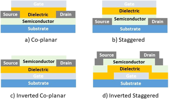
Figure 14. Cross-sectional view of basic TFT structures.
Download figure:
Standard image High-resolution image3.1. Source-gated transistors (SGTs)
Figure 15 illustrates the concept of a SGT [11, 197, 198], where a barrier at the source is used to specifically control the drain current. As a result, SGTs have a large intrinsic gain, which is independent of both voltage and geometry. This concept allows low saturation voltage, low power operation and increased stability and uniformity. The disadvantage is the lower speed due to the extra capacitance at the gate/source, and lower drive current due to the saturation at the source barrier before pinch-off in the channel. Device scaling is determined only by the channel width (W), because the source contact is shielded from the drain [11, 199, 200], and not the ratio of channel width-to-length, as in conventional transistors. SGTs therefore exhibit reduced short channel effects compared to TFTs that function in the conventional way. Performance independent of the channel length has been demonstrated down to 360 nm [174]. SGTs are especially promising for low cost manufacturing technologies because they can overcome the intrinsic processing variability of such techniques.
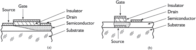
Figure 15. Comparison of electrode structure of (a) classical TFT and (b) SGT. © [2003] IEEE. Reprinted, with permission, from [11].
Download figure:
Standard image High-resolution imageSeveral non-crystalline materials have been used as active layers in SGTs [201]: a-Si:H [11, 202, 203], polysilicon [199, 204] and semiconductor oxides, in particular ZnO [200, 205]. If an additional independent gate to the channel is added to control carrier transport, known as the multimodal transistor, further functionality can be obtained [206]. Recent work shows how the key to achieving high performing SGTs lies in the optimization of the relative oxide to source capacitance [207].
We first briefly highlight some results on SGT transistors in a-Si:H TFTs, which have achieved high-performance with good frequency response and excellent stability [11]. Typical devices are fabricated by using a chromium gate metal electrode and source/drain contacts on glass substrates, a silicon nitride gate dielectric and a-Si:H deposited by plasma-enhanced chemical vapor deposition at 250°C. A phosphorus implantation is used to control the effective SB height at the source/drain. Device characteristics exhibit very stable drain currents with less than 2% variation when applying constant gate and drain voltages at 30 °C for 24 h. Numerical simulations show that this behavior is due to a decrease of the SGT carrier concentration at the source end because of the formation of a depletion region. The higher electric field near the source also contributes to a reduction in the transit time and a corresponding increase in the cutoff frequency (up to 1 MHz). Higher values of the cutoff frequency can be achieved by decreasing the dielectric and the a-Si:H layer thicknesses. Sporea et al [197] reported that the use of a self-aligned polysilicon-based SGT architecture could result in an intrinsic gain of 1000. The device used a dielectric layer consisting of 200 nm SiNx and 200 nm SiO2, and an a-Si:H 40 nm layer, which was baked at 450 °C to obtain polysilicon. A high p-implant concentration was used to form the drain-contact regions aligned with the gate. Most notably, this architecture suppressed the kink effect and leads to a very large output resistance.
3.2. Organic TFTs
An organic TFT (OTFT) uses a thin film of organic semiconductor as the channel material. The basic OTFT has a structure similar to an SBMOFET, with a metallic source/drain contacting the organic channel. The substantially fewer carriers in organic semiconductors and the polycrystalline nature of many OTFTs result in short-channel effects at much larger sizes and feature lengths. For long-channel transistors, at several tens of microns, the RSB is parasitic to device function and has only a minor impact on the device characteristics. To function in the RF regime, however, a large reduction of the OTFT channel lengths is necessary, and the contact resistance becomes crucial [208]. In addition to this role in more conventional operation, organic devices have also been used to realize source-gated transistors. In this section we discuss both of these applications.
The first OTFT was demonstrated in 1986 by Tsumura et al [209]. The main challenge for commercially viable devices is the low mobility of the transistors. Organic TFTs can be realized in conjugated polymers and conjugated small-molecule materials, the latter having in general better mobility [210]. Single crystalline films exhibit the largest mobilities, up to 40 cm2 V−1 s−1 [211] for pentacene, but are harder to fabricate for large-area applications. A breakthrough in 2012 by Li et al demonstrated record mobilities up to 10 cm2 V−1 s−1 [212] using a method that produces large-area single-crystalline organic thin films. The most promising applications take advantage of the natural mechanical flexibility of organics to integrate different types of substrates using fabrication with relatively simple and low temperature processing (<200 °C). OTFTs are therefore highly compatible with flexible substrates based on polymers and even paper.
A schematic view of the OTFT realized in coplanar and staggered architectures is shown in figure 16. Note that in comparison with figure 14, in addition to an aluminum oxide layer, the dielectric also includes a single molecular layer, known as a self-assembled monolayer, that can be used advantageously tune the properties of the device. A voltage applied to the gate induces an accumulation layer at the insulator-semiconductor interface, forming a conducting layer of holes or electrons, depending on the polarity of the gate bias. The polarity of the device depends on the type of carriers that can be injected from the electrodes into the channel region. If the Fermi level of the metal is close to the highest occupied molecular orbital (HOMO) of the organic material, then the injection of holes is enabled for a p-type device, as illustrated in figure 17. In contrast, if the Fermi level of the source is close to the lowest unoccupied molecular orbital (LUMO), an injection of electrons is possible, and the device is n-type if electron transport is possible.
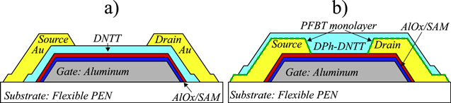
Figure 16. Schematic cross section of organic TFTs fabricated in the (a) staggered and the (b) coplanar device architecture. The gate (aluminum) and source/drain contacts (gold) were deposited by thermal evaporation or sublimation in vacuum and patterned using a high-resolution silicon stencil masks; the gate dielectric with a total thickness of approximately 8 nm is a stack of oxygen-plasma-grown aluminum oxide and a SAM [208, 213]. Reprinted, with permission, from [213].
Download figure:
Standard image High-resolution image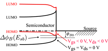
Figure 17. Energy diagrams of the interface between the organic semiconductor and the source contact of a p-channel OTFT. Application of negative gate-source and drain-source voltages increases the electric field at the SB and, according to (1), causes the barrier height to decrease due to the image charge lowering (shown in red). This effect dominates the s-shape in the output characteristics shown in figure 18. © [2021] IEEE. Reprinted, with permission, from [213].
Download figure:
Standard image High-resolution imageIn the ideal case, a matching of the HOMO in p-type devices (or LUMO for n-type) to the Fermi level of the metallic electrode would result in an ohmic contact with high conductivity and the accumulation channel alone controls the device current. In practice, the work function of the metal does not perfectly match, and a SB results bias-dependent resistance that is controlled by the gate electrode, as in an SBMOSFET. The substantially fewer carriers in organic semiconductors and the polycrystalline nature of many OTFTs result in short-channel effects at much larger sizes and feature lengths. Device operation is therefore typically restricted to several tens of microns. For long-channel transistors the RSB is parasitic to device function and has only a minor impact on the device characteristics.
To function in the RF regime, a large reduction of the OTFT channel lengths is necessary, and therefore minimizing the contact resistance is crucial [208]. At reduced channel lengths of order ∼μm, the injection of carriers at the source SB begins to have an important impact and cannot be neglected [213–217]. It results in a nonlinear S shape in the output characteristics, as illustrated in figure 18. Here, measurements on TFTs with a DNTT (dinaphtho[2,3-b:2ʹ,3ʹ-f]thieno[3,2-b]thiophene) organic semiconductor in a staggered architecture (bottom gate, top contact) are shown for a device with a channel length of 1 μm. Fitting a physics-based compact model from [213] to the measurement data results in an effective SB height at the source of ΦB0 ≈ 0.35 eV, which in the model is in series with an ohmic contact resistance of Rc Wch ≈ 117 Ωcm.
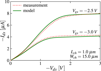
Figure 18. Calculated (green solid lines) and experimental (red dotted lines) characteristics of a staggered DNTT (dinaphtho[2,3-b:2ʹ,3ʹ-f]thieno[3,2-b]thiophene) TFT, as depicted in figure 16(a), with a channel length of 1 μm. © [2021] IEEE. Reprinted, with permission, from [213].
Download figure:
Standard image High-resolution imageThere have been several successful attempts to reduce the contact resistance and improve overall device performance. Contact doping reduces the contact resistance, possibly by reducing the width of the SB at the interface and/or by filling trap states in the organic semiconductor regions close to the contacts [218]. Another technique is to use SAMs at the interface between the contacts and the semiconductor in order to optimize the morphology of the organic material close to the contact and hence lower the SB height. A PFBT (pentafluorobenzenethiol) treatment of gold bottom contacts has successfully been applied before the deposition of the organic semiconductor for improving the charge injection across the SB [219]. This technique has allowed transit frequencies up to 21 MHz using 0.6 μm channel length transistors [208].
In summary, OTFTs have an SBFET architecture. The limitations of the SBs can be minimized by several technological approaches, which allow the accumulation channel to dominate the transport characteristics. However, if the channel length is reduced to the sub-micrometer regime, the impact of the SBs become non-negligible. One possible solution to realizing very small organic transistors is to use SGT operation [220], as discussed in section 3.1. In this case the channel does not limit the transport and the appropriate design of the transistor has shown to allow excellent characteristics down to sub 400 nm [174]. Nevertheless, SGTs will in general not be able to attain speeds as high as devices operated in conventional TFT modes due to the large gate-source depletion capacitance.
3.3. Metal-oxide TFTs
Oxide semiconductor TFTs are promising devices for large-area electronics due to their compatibility with flexible substrates, low-temperature processing, higher electron mobility compared with OTFTs, and high stability. An 32-bit ARM processor has already been demonstrated in this technology [221]. The main disadvantage of oxide TFTs is that p-type TFTs have much lower mobilities and although realization with p-type organic semiconductors have been demonstrated, to date the technologies are too different to make integration in foundries viable. Like organic semiconductors, the transistors ressemble SBMOSFETs with a metallic source/drain contact, but in their regime of operation the SB is rendered unimportant. Like organic TFTs, they have been considered as SGTs.
Metal-oxide TFTs were first demonstrated with SnO2 [222]. Investigations in this area gained traction after the discovery of colossal magneto-resistance in La–Ca–Mn–O thin films [223] and the subsequent increased interest in oxide films deposited using techniques such as pulsed laser deposition. The demonstration of a transparent ferroelectric TFT on a SrTiO3 substrate [224] is particularly noteworthy. In addition, the increasing importance of transparent electrodes for flat-panel displays, solar cells and organic light-emitting diodes, also led to research on improving the materials for the semiconducting channel in TFTs [225]. A breakthrough occurred in 2003 with the demonstration of single-crystalline indium gallium zinc oxide (IGZO) n-type TFTs with high mobilities (80 cm2 V−1 s−1) [226], and the subsequent demonstration of TFTs on a flexible foil [227].
Amorphous IGZO TFTs are now able to realize mobilities higher than 10 cm2 V−1 s−1, Ion/Ioff ratios higher than 107 and SSs close to the ideal value [228–233]. Figure 19 depicts the geometry of a recently demonstrated device. The performance of n-type amorphous (a)-IGZO transistors have been used for high-end active matrix LED displays. Their performance depends on whether the material is vacuum deposited (average mobilities >20 cm2 V−1 s−1) [234] or solution-based n-type metal-oxide TFTs (average mobilities ≈10 cm2 V−1 s−1) [235]. Because p-type oxide TFTs have generally shown much lower mobilities, although up to 5 cm2 V−1 s−1 have now been demonstrated [235], organic TFTs may provide a complementary solution for realizing more complex computing devices [236]. Source-drain ohmic contacts are, of course, the most often pursued on IGZO, and their quality depends on the contact material [234, 237]. In most cases, the electrodes are metallic, although indium tin oxide (ITO) has also been used, in particular for transparent devices [238]. An excellent overview of this technology is given in [178].
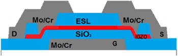
Figure 19. Cross section of the IGZO TFT fabricated at TNO. ESL is the etch stop layer and is made of SiOx . Reproduced from [228]. CC BY 4.0.
Download figure:
Standard image High-resolution imageSGTs have also been considered in oxide transistors [239]. ZnO SGTs were a natural choice because of its high electron mobility, wide band gap, good stability, easy low-temperature synthesis, and high breakdown fields [240]. As in other SB devices, below a certain gate voltage, a transition from TE to tunneling occurs [241] (figure 20). As in unipolar SBMOSFETs, this transition voltage can be identified with the threshold voltage in ZnO SGTs, since at that bias value the SB is thin enough for carriers to easily tunnel though it, therefore significantly increasing the drain current and turning the device on.

Figure 20. (a) Left: CV characteristics of the ZnO TFT measured from the gate to source electrode at VDS = 0 V. Right: Transconductance versus VGS characteristics at VDS = 7 V (long dash) and VDS = 50 mV (short-dash). (b) Energy band diagram of the Schottky SB TFT at zero VDS and zero VGS. (c) Energy band diagrams showing the variation in the width of the source barrier and the dominant carrier injection mechanism at the source with varying VGS. Please note, that as depicted in more detail in figure 17, the barrier height to the source junction will be lowered by the image charge effect for increasing gate voltage overdrive and drain bias, which boosts the tunneling current. Reprinted from [241], Copyright © 2012 Elsevier Ltd. All rights reserved.
Download figure:
Standard image High-resolution imageSB IGZO TFT fabrication is more challenging than ZnO SGTs, because of the difficulty in achieving both the high channel conductivity and the low SB heights required for its operation. In [242] an SB IGZO TFT was demonstrated. To create a Schottky contact at the source/drain contact of the IGZO TFT, the electron concentration in the IGZO film was reduced by means of a high oxygen-gas partial pressure (against argon-gas), during an RF sputtering process (figure 21). Thermal annealing was carried out to achieve a more reliable contact. The properties of the SB were exploited in deep subthreshold and low-voltage operation, with an intrinsic gain as high as 400, which is very promising for analog signal-processing applications. In this work, the effective barrier lowering at the source is responsible for a decrease in the SB width and an increase in tunneling current. It accounts for the higher transconductance in the SGT versus the conventional IGZO devices. Further studies of IGZO SB contacts found that the reverse current is drastically dependent on the IGZO thickness, which seems to be related to the inhomogeneous nature of the SB height. IGZO SGTs with extremely high intrinsic gain were reported in [174]. In that work, 10–100 nm thick IGZO films were grown on SiO2-Si wafers with 100 nm thick SiO2. RF sputtering was also applied for Pt deposition as source/drain contacts. As the IGZO thickness decreases, the threshold shifts towards positive gate voltage, due to an easier depletion of the thinner IGZO layer.
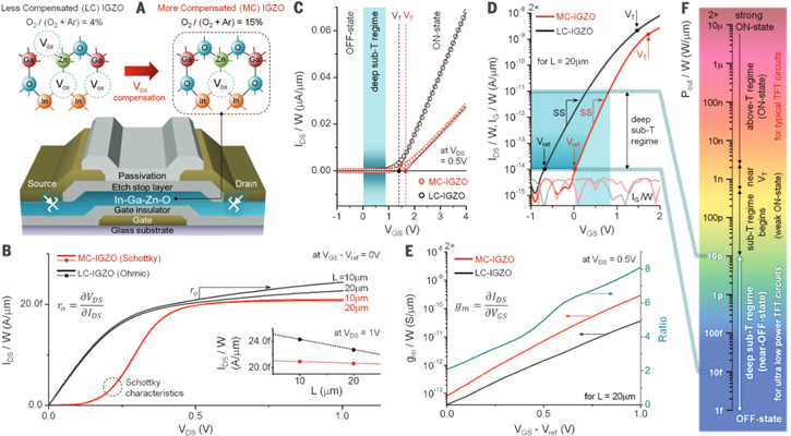
Figure 21. (a) Cross section of an IGZO TFT where the inset shows the atomic structure for the two types of devices investigated: less compensated (LC), which results in an ohmic contact and more compensated (MC), which results in a Schottky contact. (b) linear and (c) logarithmic source drain characteristics, (d) transfer curves and (e) gm−V characteristics of the two types of devices. From [242]. Reprinted with permission from AAAS.
Download figure:
Standard image High-resolution imageGraphene has also been used to change the contact properties between the IGZO layer and the metal electrode. In [243] a tunneling-contact SGT with a graphene interlayer between amorphous IGZO and Ti electrodes was reported (figure 22). In [244] a graphene monolayer was applied to create Schottky contacts with Ti electrodes. This graphene monolayer formed an effective potential barrier of 0.2 eV. In these graphene-tunnel SGTs the SS temperature dependence decreased as the drain current was increased. This suggests that the dominant electron transport mechanism changes from TE to quantum tunneling.
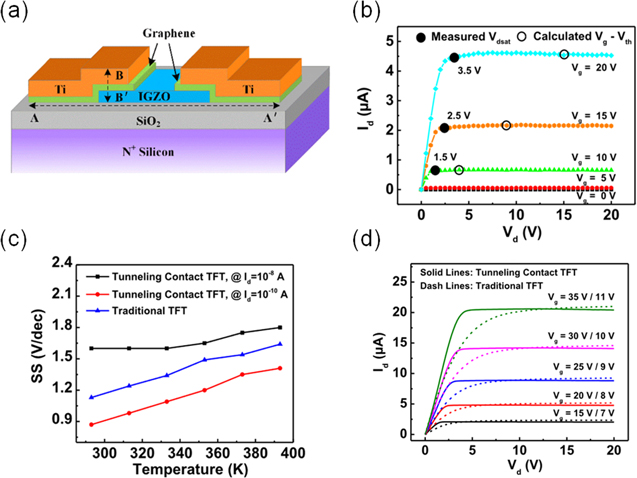
Figure 22. Cross section, I–V characteristics and sub-threshold swing of the graphene tunnel SGT reported in. Reprinted from [245], with the permission of AIP Publishing.
Download figure:
Standard image High-resolution image3.4. Nanomaterial TFTs
Bottom up emerging technologies, which have great potential for high performance computing, are often hampered by technological challenges. For 2D materials, one such challenge is the large contact resistance. For SWCNT devices, it is the realization of arrays containing only semiconducting nanotubes. The relaxation of the performance metrics due to such challenges provides these technologies possible applications in ubiquitous electronics. Here, we discuss briefly some of the ways that have been investigated.
A new class of nanocomposite TFTs have emerged in the past twenty years based on thin films of chemically synthesized nanomaterials. The basic constituent can be thin films of nanocrystals, nanowires or nanotubes. The electronic transport resembles neither that in the nanomaterial, nor transport in the bulk, but is typically dominated by the transport between nano-objects and can be described by percolation models [246]. Nanonet TFTs [247] are a fascinating topic and have been the subject of a recent review [79], although for most materials the source/drain contacts do not play an important role in the transport.
Nevertheless, it is important to mention the emerging field of TFT transistors fabricated using carbon nanotube networks. CNT TFTs can broadly be grouped into those where the channel length is about or greater than the tube length, of relevance here, and those where the channel length is much smaller, which were discussed in previous section 2.2. While aligned nanotube arrays or single devices typically have mobilities exceeding 2500 cm2 V−1 s−1, the mobility of such thin-film transistors is ∼20–500 cm2 V−1 s−1 due to the tube-tube interactions. In these nanonet-type TFTs, the contacts at the film/source or film/drain interfaces can still play an important role either by introducing an important barrier to transport [248], or by increasing the off-state current through the ambipolar transport at the drain at higher voltages [249]. Pecunia's group has shown how the ambipolar devices can be used in ultra-low power electronics [250]. CNT TFTs have been used to realize a modern microprocessor [149] with CMOS devices and channel lengths down to 1.5 μm. To the best of our knowledge these are the highest-performing TFT computing devices demonstrated.
The SB height of CNTFETs can be strongly influenced by changing its environment (from air to vacuum), where the barrier height is strongly affected by molecular adsorption (of water and oxygen in particular) both on the metal and on the CNT [251]. Electrochemical reactions at the SiO2/nanotube interface in the presence of water and oxygen were also shown to play a significant role on the electron/hole current balance [252]. Such effects have been used to develop chemical sensors [253] and biosensors [254]
Like carbon nanotubes, SBs in 2D materials also exhibit very unique properties. The SB height (SBH) and Fermi-level pinning exhibit a thickness-dependent phenomenon [243], providing an exciting playground for engineering nanodevices and novel sensors. This is reminiscent of the observation that the Richardson constant changes with film thickness, as discussed in section 1.2. For large work-function metals, p-type SB contacts have been shown to be more favorable. This thickness dependence provides a parameter to manipulate the SBH in metal-2D semiconductor interfaces, illustrated by the SBHs in table 1. Research on 2D materials has focused on realizing transistors and explorations in ubiquitous electronics are just beginning to emerge. Sensor-based technology for health and the environment also have been developed to take advantage of the ability to control the SB [255]. Another field of application related to the ambipolar nature of the contacts is reconfigurable transistors for secure circuits, as discussed at the end of the next section.
Table 1. The SBH  of the nth MoS2 layer in a 7-layer AgMoS2 junction. Vn−1,n
is the energy difference between the conduction band minimum (CBM) in adjacent layers, which shows the depinning between MoS2 layers.
of the nth MoS2 layer in a 7-layer AgMoS2 junction. Vn−1,n
is the energy difference between the conduction band minimum (CBM) in adjacent layers, which shows the depinning between MoS2 layers.  = CBMn
− EF; Vn−1,n
= CBMn
− CBMn−1. (All values are given in eV). These calculated values are taken from [243].
= CBMn
− EF; Vn−1,n
= CBMn
− CBMn−1. (All values are given in eV). These calculated values are taken from [243].
| nth MoS2 layer |

| Vn−1,n |
|---|---|---|
| 1st | 0.14 | — |
| 2nd | 0.30 | 0.16 |
| 3rd | 0.42 | 0.12 |
| 4th | 0.52 | 0.10 |
| 5th | 0.56 | 0.04 |
| 6th | 0.57 | 0.03 |
| 7th | 0.58 | 0.01 |
3.5. Reconfigurable transistors
SBMOSFET devices with mid-gap SBs and intrinsic or low-doped Si have a considerable SB for both electrons and holes., [80]. These devices have an SB for both electrons and holes, delivering an ambipolar transfer characteristic, i.e. allowing for the injection of both electrons and holes for positive and negative gate voltages respectively as shown in figure 23(a). This behavior differs significantly from that described above. Figure 23(b) shows the calculated transfer characteristics from TCAD simulations. NiS2/Si junctions were modeled and both TE and tunneling transport were taken into account.

Figure 23. Schottky barrier MOSFET with intrinsic-Si/NiSi2 junctions, exhibiting considerable barriers for holes and electrons and therefore delivering ambipolar I–V behavior.
Download figure:
Standard image High-resolution imageTo explain the underlying transport, band diagrams for such midgap aligned contacts are shown in figure 23. The transfer characteristics, plotted in a semi-logarithmic representation, generally exhibit two distinct regions below threshold voltage, which are separated by a characteristic kink: (a) a steeper and linearly increasing one for low drain currents and (b) a shallower and progressively saturating region at higher drain currents. As indicated by TCAD simulations, for Id the predominant injection mechanism is, in region (a), TE and in region (b) thermally assisted field emission (TFE). Kedzierski and Knoch [59, 256] showed that the TE region generally has a steeper SS than the tunneling dominated (TFE) region. In the TE case the potential barrier maximum is displaced linearly by the acting gate field as in a conventional MOSFET. However, in the case where TFE is dominant, the bands at the injecting junction drop below the SB height so that the barrier maximum remains fixed and only the thickness of the SB and thus the tunneling probability is modulated, delivering typically shallower SSs. As a result, the magnitude of the threshold voltage is substantially increased compare to that of conventional MOSFETs. Both the ambipolarity and the threshold voltage degradation of Schottky FETs can be addressed by manipulating the potential across the active region through the application of independently gated regions, as shown in section 3.5 for reconfigurable nanowire transistors.
Ambipolar SB MOSFETs have also been demonstrated with NiSi2/intrinsic Si nanowires following the injection mechanism [162] described in figure 23. Both the ambipolarity and the threshold voltage degradation of Schottky FETs, as discussed in section 1.3, can be addressed by manipulating the potential across the active region through the application of independently gated regions, as discussed next for reconfigurable transistors.
Reconfigurable transistors (RFETs) are an emerging type of device family based on Schottky source and drain junctions applied to an ultrathin-body semiconductor (1D or 2D) that are capable of delivering unipolar p- and n-channel MOSFET functionality as deterministically selected by an electric signal. A complete review of the transport properties, device types and emerging circuit applications can be found in [257–259]. To define the device polarity, RFETs are able to filter out a specific unwanted polarity of charge carriers by the introduction of a potential barrier within the active region. A dedicated gate electrode commonly labeled as the polarity gate (PG) is employed to control this barrier, whereas the charge carrier flow is regulated by an additional electrode, the control gate (CG). Different RFET realizations exist; in the simplest embodiment, the two independent gates are positioned to directly overlap the SB junctions, deliberately defining the CG and PG. The gated Schottky diodes allow respectively for efficient injection control at the source [260, 261] and for polarity adjustment at the drain by blocking the injection of the undesired carrier type, see figures 24(a)–(c). This 'dual gated' RFET approach was realized in heterogeneously integrated Si nanowires with intruded NiSi2 contacts [12, 262], Ge nanowires with Nix Ge1−x [263] and Al electrodes [264], as well as in Six Ge(1−x) nanosheets with Al contacts [166]. In addition to its geometric simplicity and doping-free fabrication flow, the device exhibits a very low static power consumption, with gate induced drain lowering-like leakage suppressed even for higher source-drain bias. Nevertheless, the threshold voltage remains comparatively high for the same reason as in single gated SBFETs.

Figure 24. Operating principle of the reconfigurable Schottky MOSFET (RFET). First column (a)–(c) shows the embodiment and operation as a dual independently gated RFET and the second column (d)–(f) shows the triple independent gated RFET. The first row shows the schematic technological realizations, below are the schematic band diagrams for different operation regimes. Note that e) and f) show respectively the n- and p-type program for different CG potentials.
Download figure:
Standard image High-resolution imageTo improve the SS, a second RFET embodiment called here the 'triple gate' RFET can be found in the literature. It employs three independently gated regions [164, 265–272]. Therein, both SB junctions are steered with the same potential as the PG that defines the predominant charge carrier type, while the 'middle segment' of the channel is itself steered by the CG, see figures 24(d)–(f). Since the potential at the SB junctions are decoupled from the CG by the shielding action of the PG, the subthreshold behavior is governed by the barrier maximum within the CG-steered segment, as in a conventional MOSFET. Compared to the 'dual gated' RFET, the 'triple gate' one has a higher static power consumption in the off state. Both RFET realizations however show smaller on currents than MOSFETs and therefore have a longer switching delay. The targeted applications are thus in the field of low standby and low operation power applications. Performance enhancement with respect to Si is expected with the use of Ge channels [271, 273] as TE and TAT become more efficient due to the smaller SB heights and smaller effective tunneling masses.
The benefit of RFETs becomes visible when the inherent reconfiguration feature is exploited at runtime to enable fine-grained reconfigurable circuits. Generic logic gates and circuits can thereby alter their functionality at runtime, e.g. between NAND/NOR/MIN [274] or XOR/XNOR/MAX [269], reducing overall chip area consumption [275] and enabling new opportunities for camouflaging circuits for hardware security applications [276, 277], as well as embedded electronics.
Some 2D materials exhibit ambipolarity where the SB or electrostatic gating can allow either p-type or n-type transport. This was first exploited to realize electrostatically reversible polarity using a dual top gates [278] and then complex logic gates [279] in MoTe2. More recently these ideas were extended too demonstrate more complex circuits and neuromorphic functionality [280], secure applications [272] and reconfigurable logic integrated with optoelectronic transistors [281].
4. Applications of SB devices at cryogenic temperatures
Cryogenic electronics has typically been a niche field, used for applications such as astronomy and detectors for particle accelerators. Despite better device performance at low temperatures, for mainstream electronics it has never been a viable option because of the power consumption required to cool the devices. More recently however, the increasing importance of quantum information processing has revitalized this field, which has now made its appearance in the IRDS [282].
SBMOSFETs can play a role in two ways. The first is in cryo-CMOS because of the simpler and lower-cost fabrication and the conducting metallic contacts that do not freeze out at low temperatures like non-degenerately doped source/drain regions. SBMOSFETs have not yet been explored in this context. The second is to use metallic source/drain electrodes that become superconducting at low temperatures. Superconductivity is a macroscopic quantum phenomenon and its introduction into transistors fundamentally changes their physics, behavior and device optimization. This is the main subject of this section. We first review cryogenic electronic transport in SBMOSFETs and superconductivity in section 4.1, discuss their applications in section 4.2, before addressing their optimization in section 4.3 and the special role that SB devices can play in section 4.4.
4.1. Transport at cryogenic temperatures
As temperature is reduced in crystalline semiconductors, the mobility of carriers increases significantly due to a reduction in phonon scattering. This effect gives rise to an increasing 'on' current and in Si transistors continues until about 100 K. Concomitantly, the number of carriers decreases exponentially, giving rise to an increase in the threshold voltage and a sharper SS, as shown in figure 25. Below 100 K, the majority of carriers are frozen out and various interesting physical phenomena can be observed, such as weak and strong localization, phase transitions, universal conductance fluctuations, Coulomb blockade and resonant tunneling through impurities. Such effects are seen in SBMOSFETs, but in addition the SB plays an important role in the transport. As the temperature is reduced from 300 K, current transport mechanisms across the Schottky junctions become decreasingly dominated by thermal processes until they are dominated by direct tunneling, as in Schottky diodes [9]. The dominant scattering mechanism in the mK temperature range and at low bias voltages is electron–electron interactions [283], which can give rise to a zero-bias anomaly [284]. The dopants in silicon can be frozen out [285], but the advantage of the SB device is that carriers in the metallic contacts (as opposed to non-degenerately doped source-drain ones) are not. For SBMOSFETs with relatively large widths, the SB can also be used to energetically isolate a single or small number of dopants, allowing a rich exploration of physics [286–289]. Figure 25 shows characteristics at 300 K and 4 K of an SBMOSFET device with PtSi contacts, which have a critical temperature Tc ≃ 0.8 K for film thicknesses above 20 nm [290]. At room temperature, the SS follows the expected thermally activated law and differs only minimally from the ideal 60 mV dec–1, revealing a good control of the channel carrier density.
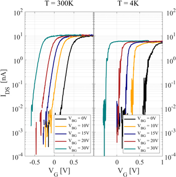
Figure 25. Characteristics of a PtSi-based SBMOSFET on FDSOI, fabricated using standard CMOS technologies [55, 56] with a buried oxide layer (BOX) of 145 nm and a slightly n-doped channel (800 nm wide by 60 nm long). The silicon substrate can be used as a back gate, in addition to the top gate. The back gate operates at low temperatures with the help of illumination in order to generate carriers in the silicon wafer. (Left) Source/drain current Ids vs top-gate voltage Vg at room temperature for various values of the applied back gate voltage Vbg, with Vd = 100 μV. (Right) The same measurements, now at 4 K. Note that the current fluctuations are completely reproducible.
Download figure:
Standard image High-resolution imageAt 4 K, Ion changes from 10 to 6 nA at a Vds = 100 μV, and the SS becomes steeper (though less than expected at 4 K). These observations indicate that the transport is limited by the source/drain contacts. At very low voltages, the observed small reproducible oscillations can be attributed to the Coulomb blockade of residual dopants that are either in the channel [291] or near the source/drain contacts [287].
Interesting and different characteristics are observed if the metallic contacts become superconducting. Superconductivity is a macroscopic quantum phenomenon, in which a phonon-mediated pair-wise attractive interaction between electrons causes a large fraction of the Fermi sea to condense into a lower-energy state [292, 293]. It causes the opening of a symmetric gap around the Fermi level in the energy spectrum and at T = 0 K, it has a magnitude of 2Δ ≈ 3.53kB Tc [292]. The energy scales important here are much smaller than those typically encountered in semiconductor physics: the superconducting gap Δ ranges from 3 × 10⁻⁴ eV (Al) to 3 × 10⁻³ eV (Nb), the most commonly used superconductors for the devices of interest here [294], and superconducting devices operate at temperatures 3–5 orders of magnitude below room temperature. When kB T ≪ Δ, the transfer of individual carriers from the semiconducting channel to the superconducting contacts is forbidden by the gap in the superconducting single-particle energy spectrum.
Transport is possible however, through a process called Andreev reflection [295], in which an incident electron from the normal material picks up an additional electron at the interface and continues as a Cooper pair inside the superconductor, while the resulting hole precisely traces back the incoming particle's path on the normal side [295–297]. The resulting 'leaking' of the superconductivity into the normal metal is referred to as the proximity effect, and induces a smaller minigap inside the channel [298, 299]. Figure 26 shows that at temperatures well below the superconducting transition of PtSi, the differential conductance exhibits a clear dip at zero Vd bias followed by symmetrical peaks around Vd = ±160 μV. The insert of figure 26 shows how the voltage at which the peaks appear evolves with temperature: It follows the expected reduction of the superconducting energy gap [292], represented by the solid line, from which we can extract the superconducting transition temperature Tc = 0.67 K of the PtSi contacts. The device essentially has two superconducting/semiconducting (S/Sm) interfaces in series, such that the peak position Vpeak should be twice the superconducting gap. Extrapolated to zero temperature, Vpeak = 0.163 mV, which differs by 20% from the value expected from the BCS relationship Δ = 3.5kB Tc/q [292, 300]. This theoretical gap value corresponds to the gap deep inside the superconducting material, and can be different at the S/Sm interface due to the proximity effect.
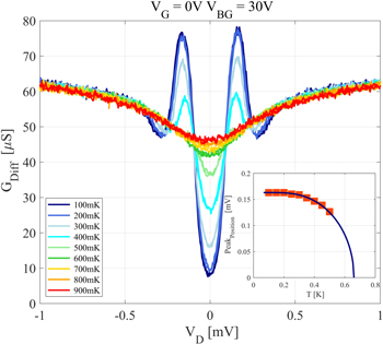
Figure 26. Low-temperature differential conductance of a silicon transistor with superconducting PtSi contacts. Insert: temperature dependence of the coherence peak voltage, together with the fitted BCS superconducting gap temperature evolution (solid line) [292].
Download figure:
Standard image High-resolution imageThe rate at which Andreev reflection occurs, depends strongly on the interface transparency of the S/Sm interface and the height of the SB [301], which is why these measurements were performed with sufficiently large Vg to be in the 'on' state of the transistor. Since the coherence of the Andreev pair also depends on scattering within the channel, a large Vbg was applied as well. If the retro-reflected hole can propagate in the channel and be itself retro-reflected as an electron at the second S/Sm interface, then this closed loop will generate a bound (Andreev) state that can carry a supercurrent, causing the conductance to diverge, as illustrated in figure 27.
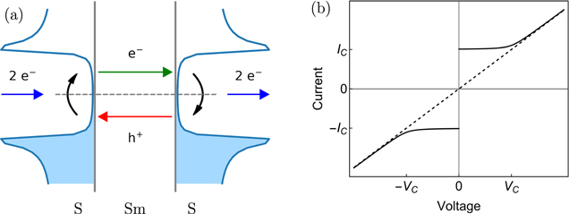
Figure 27. (Left) Illustration of a superconducting/semiconducting/superconducting (S/Sm/S) junction. The densities of states are drawn for the superconducting leads, and a dashed line indicates the Fermi level. A Cooper pair is transferred across the channel as an electron–hole pair, before forming a new Cooper pair on the other side. Note that the hole is moving in the opposite direction: the hole component of the pair travels as an electron, but 'backward in time' [296, 297]. Reproduced from [302]. (Right) This process allows current to flow in the absence of a source-drain voltage.
Download figure:
Standard image High-resolution imageIf the coherence of the Andreev pairs is strong enough such that the Josephson coupling EJ = ℏ Ic/2e, where Ic is the critical current, is greater than the thermal energy kB T, then the semiconducting channel will act as the weak link in a Josephson junction [303]. At this point, the probability of the Andreev pair entering the superconductor on the other side would depend on the phase difference between the two condensates [299, 304]. Once a Josephson coupling is established, the coherent transport creates a zero-resistance channel [305–307] such that a current can be applied without generating a source-drain voltage (the DC Josephson effect, see figure 27(b)), while an applied voltage will cause the current to oscillate (the AC Josephson effect) [308]. Note that the device in figure 26 exhibits a decrease of the conductance at zero bias, implying that the quality of the interface is not good enough to observe Josephson tunneling. Nevertheless, the fact that the conductance stays finite at zero bias, indicates that transparency is partially achieved.
4.2. Applications for superconducting SBFETs
If superconductivity can be transmitted through the semiconducting channel of SBMOSFETs with superconducting source/drain electrodes, then a Josephson FET (JoFET) is realized, where the modulation of the carrier density in the channel and SB height can control the critical current [303, 309]. It has been demonstrated that a semiconducting channel with high transparency to the superconducting leads can be used to provide a tunable Josephson coupling for superconducting qubits [310, 311]. Semiconducting channels that are small enough to behave as quantum dots have revealed a rich variety of charging phenomena [312]. Devices with larger [313], metallic channels no longer exhibit the Josephson effect, but the superconducting gap can be used to extract the hot tail of the Fermi–Dirac distribution and thus locally reduce the electron temperature [314].
This research area has recently become sufficiently mature to be of industrial interest; quantum supremacy was achieved in a superconducting system in 2019 [315], and several industrial laboratories have now published roadmaps towards quantum computers with millions of qubits [316–318]. The Josephson junctions on which these devices are built provide a dissipationless nonlinear inductance to a circuit that can be approximated as an LC resonator with quantized excitations. The nonlinearity ensures that the spacings between successive energy levels are different (i.e. the system becomes anharmonic), such that the lowest two can be isolated as an effective two-level system and serve as a qubit. Control of the interactions between multiple qubits requires the tuning of either the resonance frequencies of these circuits themselves, or that of a coupler placed between two fixed-frequency qubits. This tuning is accomplished by varying the inductance, most commonly by running a current through a nearby line to apply a magnetic flux to a superconducting quantum interference device (SQUID) made up of a pair of Josephson junctions. Alternative designs have been demonstrated where nanowire-based JoFETs replace these flux-modulated SQUID loops, creating gate-tunable transmons that rely on a static voltage instead of a continuous current [310, 311], with the advantages of reduced dissipation, cross talk, and flux noise. Lithography-based two-dimensional JoFETs [319, 320] provide the additional benefit of easier scaling, and fit in the trend of integrating CMOS technologies such as 3D routing with through-silicon vias (TSVs) and multi-level wiring in quantum circuits [321].
These experiments have typically been realized with academic fabrication techniques such as aluminum lift-off[312], electron-beam lithography of the junction areas [322], or the use of materials such as InAs and GaAs [323]. It remains to be seen if a modern transistor could be modified to perform the same tasks, and if so, what precisely would have to be changed for it to perform optimally [302]. Such mass-manufacturable JoFETs could have a large impact especially in the fast-growing field of superconducting qubits.
4.3. Optimization of superconducting devices
FETs are typically optimized for large on/off current ratios, short switching times, low energy dissipation and small footprint. Most of these concerns are irrelevant for JoFET applications. In a superconducting qubit, the supercurrent is varied by only a few percent during operation to change the Josephson coupling [310] and large on/off ratios are not essential. Concerning the switching times and low energy dissipation, in a JoFET the capacitance of the junction itself is far smaller than that of the qubit to which it provides the inductance, and therefore the LC time  to discharge the channel is guaranteed to be short enough for qubit control. The superconducting state of the circuit ensures that RC times are zero, and that dissipation is minimal even at high frequencies. The fabrication of JoFETs instead seeks to realize devices with critical currents on the order of tens of nA [310], few two-level systems [324, 325], little quasiparticle tunneling [326], and low sensitivity to flux noise in the channel or charge noise on the gate electrode. Apart from the last requirement, which is less stringent in the today's most common type of superconducting qubit [327], these aims are all helped by increasing the supercurrent density of the JoFET, as we now discuss.
For the phase information of the superconducting condensate in one lead to be coherently transmitted to the other, a few processes need to occur successively. First, Andreev reflection requires that both the incoming and outgoing particles tunnel through any potential barriers present between the superconductor and semiconductor. A good intuition for this process can be gained by considering the WKB approximation for the tunneling of a particle. If we assume, for simplicity, a square barrier potential of height ϕ and width d, we find that an incoming electron has a transmission probability (transparency)  , which for an undressed electron with m⋆ = me, a barrier of height ϕ = 0.1 eV and width d = 1 nm, equals roughly
  . Since the reflected hole would have to traverse the same region, we naively expect that the entire process of Andreev reflection occurs with probability
  (a more comprehensive calculation based on the BTK formalism [301] would find
  when
when  ). The salient point here is that Andreev reflection is exponentially suppressed by an increase in SB height, with about twice as a large an exponent as a single-particle tunneling process, making it critically important to obtain a transparent interface, as in section 1.3
Once Andreev reflection has occurred, an effective energy gap  will be induced on the semiconducting side of the interface, where Δ is the gap in the bulk superconductor and δ the factor by which it is reduced (δ ∝ T2 in the above approximation). The Andreev pair then has to traverse the channel, during which the electron and hole will dephase due to accumulated differences in energy, and finally a second reflection needs to take place in order to enter the opposing lead. Intuitively, one may expect that the critical current of the junction, which is proportional to the combined likelihood of this entire string of events, would scale as δ2 and drop exponentially with the length of the channel [305, 306],

where ξSm is an effective coherence length for the Andreev pair inside the semiconductor. Although this exponential decay is an accurate depiction of thermal effects [303, 328, 329] when we replace  , where D = vF
ℓe/3 is the diffusion constant, it does not fully capture the physics of longer channels. For diffusive junctions (L ≫ ℓe), the relevant energy scale for the proximity effect turns out to be the Thouless energy
ETh = ℏ
D/L2 [330, 331], where ETh/ℏ is the rate at which single charges diffuse across the channel [307]. Unless the superconducting gap Δ is smaller than ETh, this diffusion rate will then limit the supercurrent that can cross the channel (before thermal effects are taken into account), as is shown in figure 28. We can thus summarize the zero-temperature behavior as:
, where D = vF
ℓe/3 is the diffusion constant, it does not fully capture the physics of longer channels. For diffusive junctions (L ≫ ℓe), the relevant energy scale for the proximity effect turns out to be the Thouless energy
ETh = ℏ
D/L2 [330, 331], where ETh/ℏ is the rate at which single charges diffuse across the channel [307]. Unless the superconducting gap Δ is smaller than ETh, this diffusion rate will then limit the supercurrent that can cross the channel (before thermal effects are taken into account), as is shown in figure 28. We can thus summarize the zero-temperature behavior as:

where the dependence of δ on the barrier strength at the interface is described by the BTK model [301]. Depending on how the thermal energy kB
T compares to Δ and ETh, a finite temperature can then be accounted for with a further factor that ranges from  to
to  [307, 332].

Figure 28. At zero temperature, the remaining limiting energy scales for the proximity effect are the superconducting energy gap Δ and the Thouless energy ETh. This means that when the junction has a large effective length, such that ETh < Δ, the critical current will be limited by the Thouless energy, while shorter junctions, with ETh > Δ, will see Ic limited by the gap Δ instead. Reprinted figure with permission from [308], Copyright (2001) by the American Physical Society.
Download figure:
Standard image High-resolution imageThese limits to the critical current can be directly translated to guidelines for the design of a good Schottky barrier JoFET (SBJoFET), which are illustrated in figure 29. The main concerns are: (a) to ensure a low barrier between the contacts and the channel, which can be achieved by using materials with good lattice matching, similar effective electron mass, clean interfaces and low SBs. Note that the SB lowering described in figure 2, should significantly aid the latter as channel lengths are made smaller; (b) The effective channel length may be reduced by downscaling the device and increasing its mobility, which could possibly bring it into the ballistic regime; finally, (c) if the Thouless energy is of the same order, or even larger than the superconducting gap of the contact material, further improvements in performance could be gained by using a higher critical temperature of the superconducting contacts.
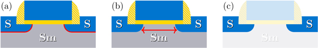
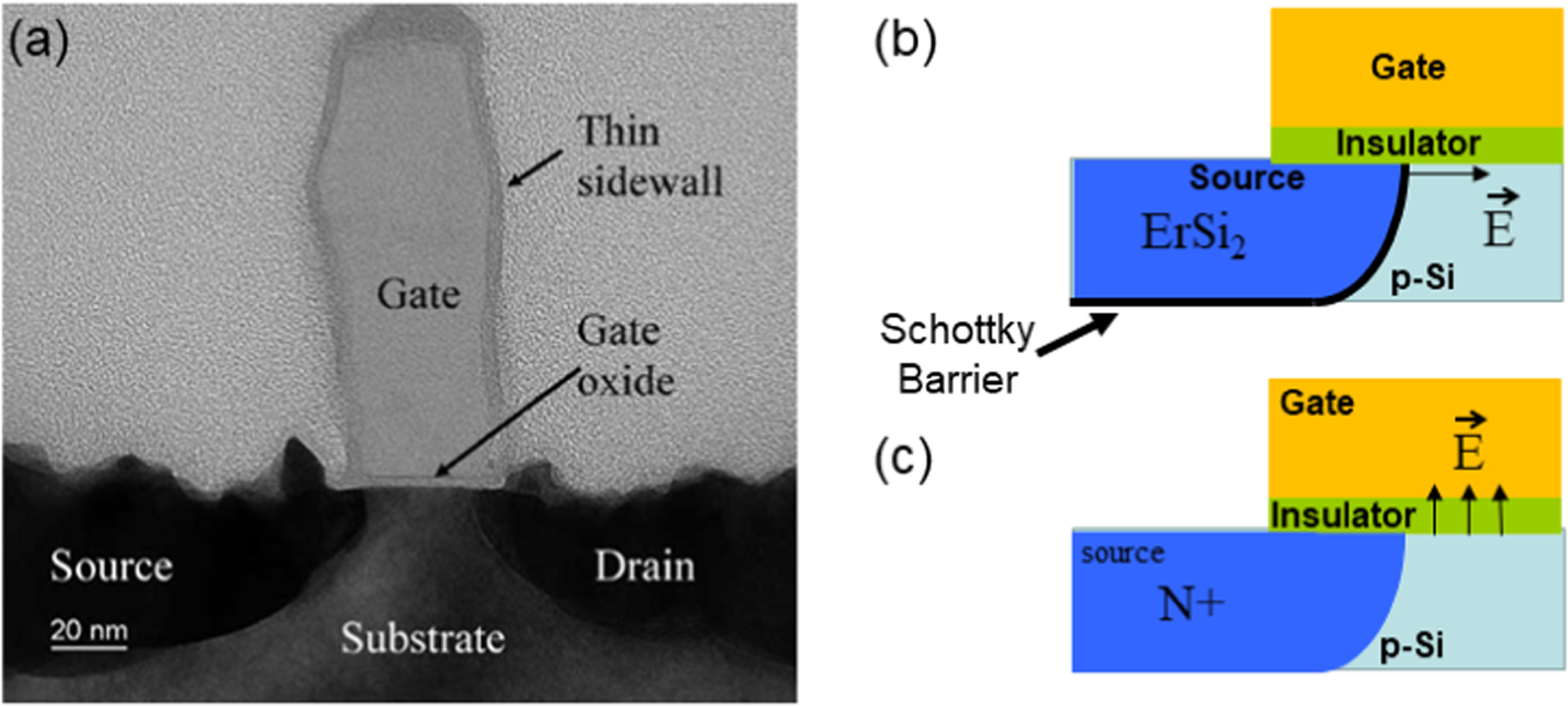
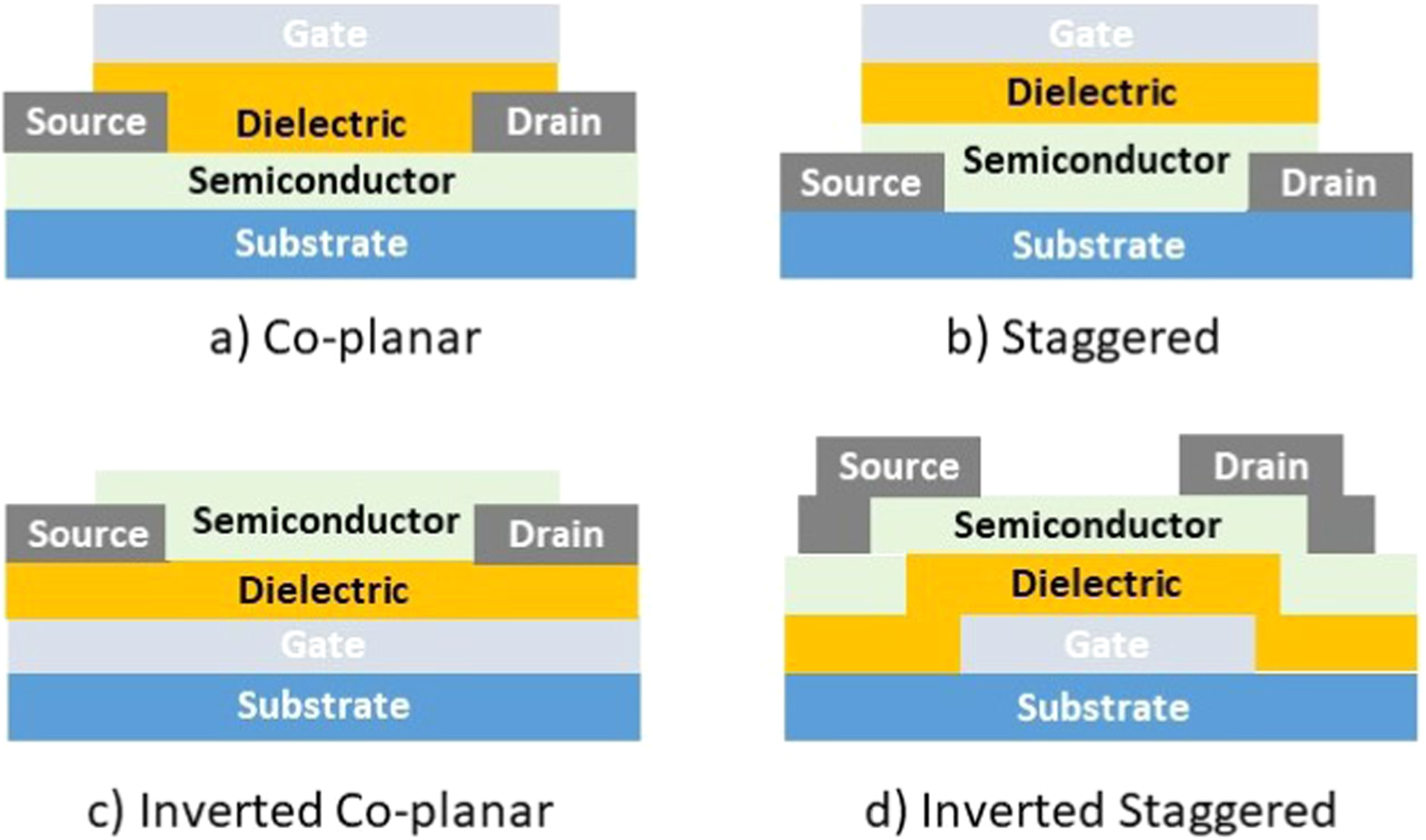
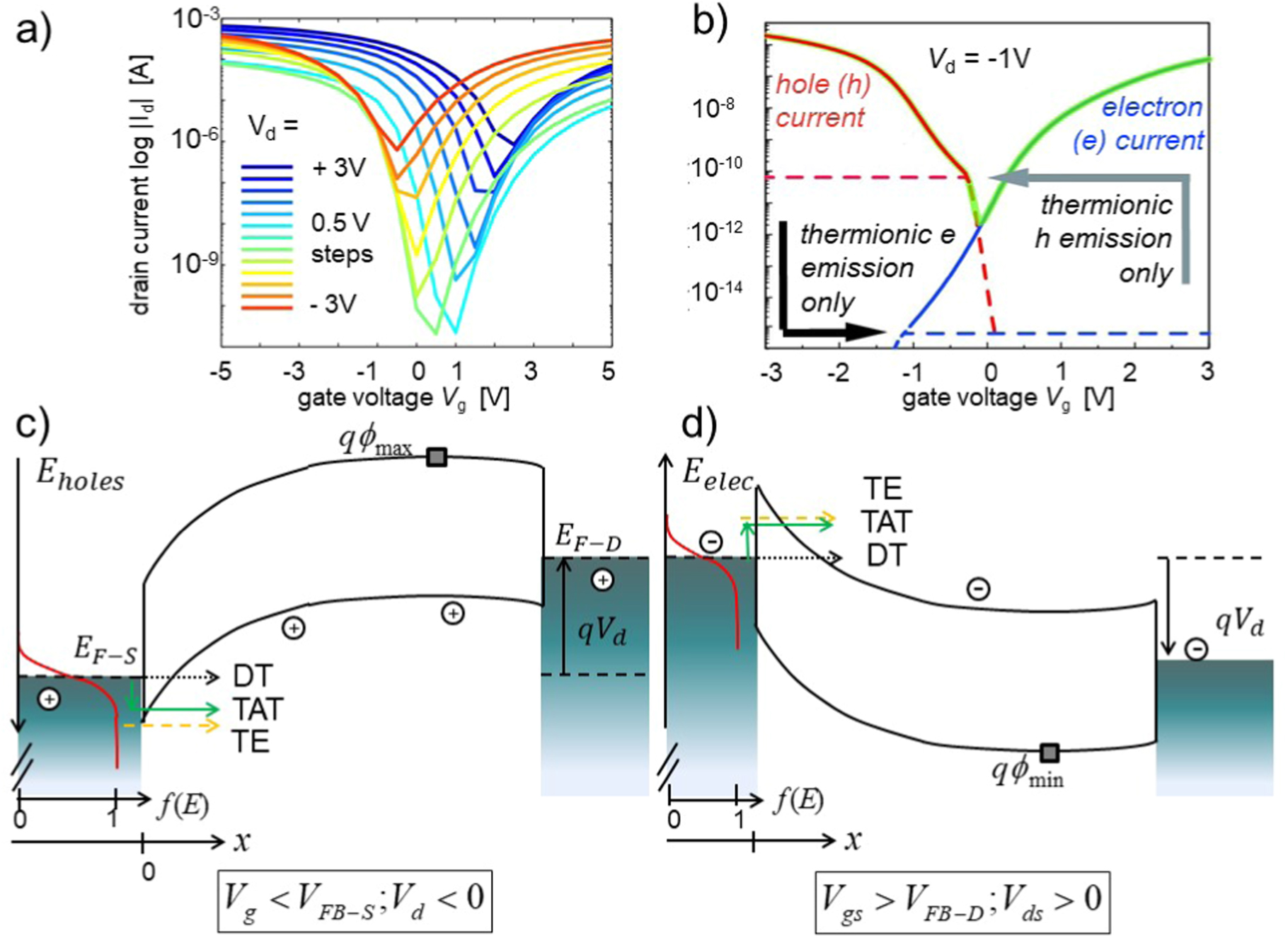
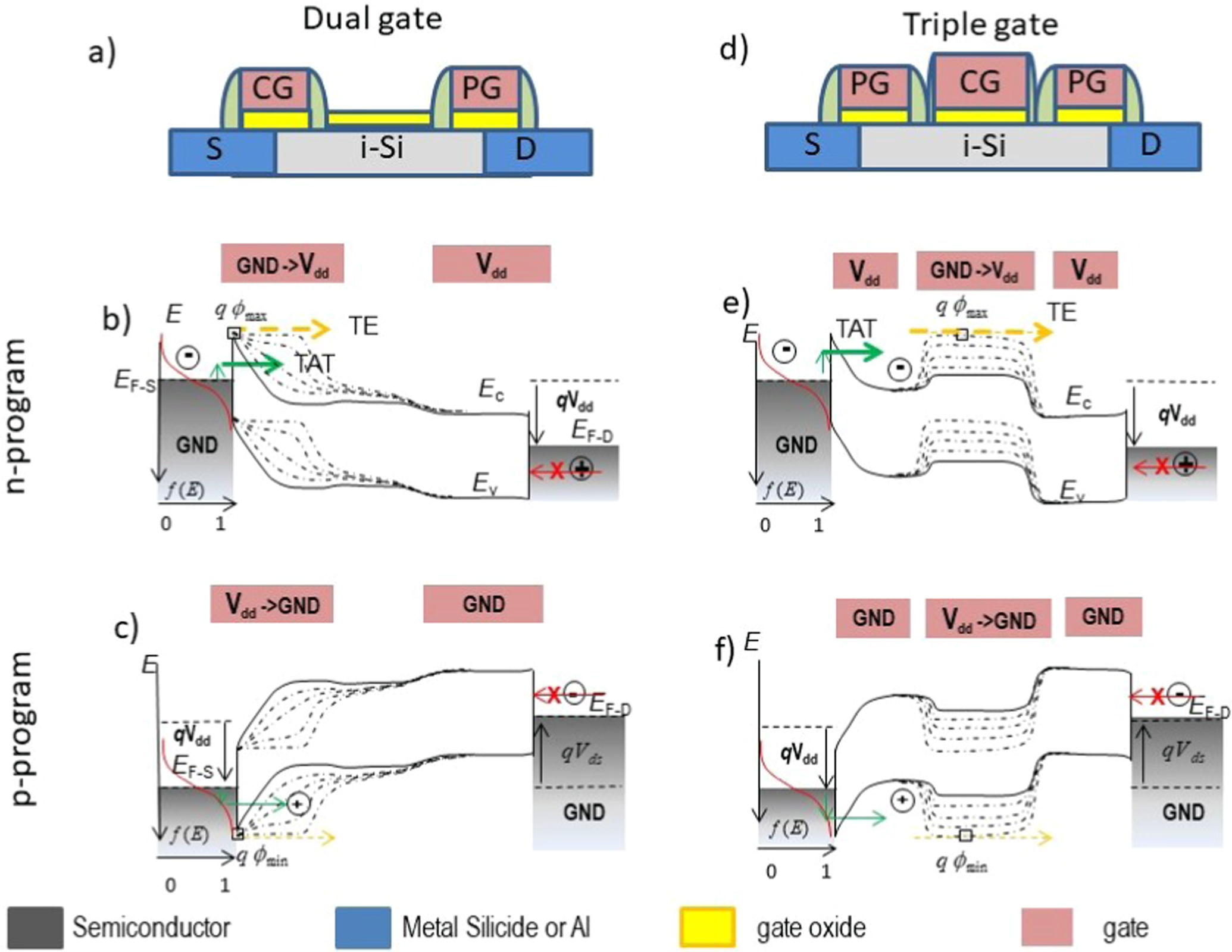
Figure 29. Three factors limit the supercurrent in an SBJoFET. The interface between the superconducting leads and the channel, depicted in (a) by the red region around the superconducting electrodes, needs to have a small potential barrier for carriers at the Fermi level. Since Andreev reflection is a second-order process, the tunneling through the barrier needs to occur twice during a single reflection. The channel length, as depicted by the arrow in (b), should be small enough so that the phase coherence of the particle and hole in the Andreev pair, which drops off exponentially, is not diminished to zero. (c) For short channels, the critical current is linear in the critical temperature of the material in the leads, which are highlighted in the figure.
Download figure:
Standard image High-resolution image
4.4. The implementation of SBMOSFETs as JoFETs
III-V materials have long been the preferred semiconductors in mesoscopic superconductivity experiments thanks to their higher mobility and the absence of carrier freeze-out at low temperatures [303, 333]. A few years after a gate-tunable proximity effect was detected as a voltage-dependent resistance jump in a Pb/p-InAs/Pb junction [334, 335], it was demonstrated that tunable coherent transport across the entire channel could also be obtained in shorter junctions [336]. The largest supercurrents to date, and some of the most transparent interfaces to semiconducting channels, have been obtained using InAs nanowires [337, 338], which became an especially attractive platform for quantum applications after sub-gap states were further suppressed by epitaxially growing the superconducting aluminum layer [339, 340]. Lithographically defined structures in planar heterostructures containing InAs films were later proposed to allow for easier fabrication of larger circuits that contain multiple junctions [319, 320]. Now, as the demand for scalability grows [341], it is natural to ask whether some of the technologies honed for MOSFET development can be put to use in this field, and whether silicon could be a viable substrate.
In fact, around the same time that it was shown in InAs [336], a gated supercurrent was demonstrated in a 200 nm long, highly doped Si channel contacted by a superconducting Pb alloy [342]. It is possible that the freeze-out of carriers was prevented by the high doping level of 5 × 1018 cm−3, and the channel may have been further populated by field emission from the superconducting leads, allowed by the overlap of the gate with the source and drain electrodes [333]. Members of the same group later contributed to demonstrating a self-aligned Si MOSFET with doped source/drain regions underneath superconducting Nb electrodes [322]. This device was closer to a conventional doped source/drain FET than an SBMOSFET due to the doping level of 5 × 1019 cm−3 underneath the superconducting contacts, without an overlap between the gate and the superconducting electrodes.
An SBJoFET could be formed instead by replacing the doped source/drain regions in this type of device by superconducting silicides, which would have several likely advantages. As discussed in section 1.3 and suggested by lower capacitance ratios [61], a significant part of the transport in an SBMOSFET occurs further away from the oxide/semiconductor interface compared to conventional MOSFETs. This should reduce surface scattering, improving the mean free path in the channel. Mobility could be further improved by reducing the channel doping, which due to the presence of SBs in the off state would no longer create the risk of short-channel effects. It is however not yet clear how well JoFETs with low doping or undoped Si would perform. Earlier demonstrations of Josephson coupling through silicon weak links used extremely high doping of 1 × 1020 cm−3 [343, 344] (corresponding to 0.2 at%) in order to boost the coherence length [345], but only devices with lower channel doping levels of 5 × 1018 cm−3 [342] and 5 × 1016 cm−3 [322] have exhibited electrostatic gating.
The use of silicides in SBMOSFETs can also provide greater control over the channel length, which can be reduced below the lithographically defined gate length by the encroachment of the metallic alloy underneath the spacers during silicidation. If this process is allowed to continue until the silicide extends beneath the gate electrode, it may enhance SBJOFET operation by significantly reducing the SB height via the image charge. This would ensure a large variation in critical current, and more importantly, provide control over the interface transparency, the main bottleneck to obtaining a Josephson coupling in JoFETs as highlighted in figure 29. Experiments on junctions with InGaAs weak links have shown that a gate effect can be used to suppress SBs up to the point that Andreev reflection dominates transport across the interface [346]. These InGaAs devices had higher doping close to the superconducting contacts [347], placing them between the doped source/drain FET and Schottky FET architectures. Such intermediate devices can also be constructed in CMOS technology by out-diffusing dopants from the source/drain regions, which provides additional control over the SB and may further improve the capacitance ratio [63]. With these options available, and more than three decades of technological progress in semiconductor manufacturing since the first demonstration of a silicon JoFET, we can be optimistic that SBMOSFETs optimized for quantum applications are within technological reach.
5. Conclusions
In this review we have seen that SB source/drain transistors permeate many emerging technologies. We have found that for high performance technologies the consensus is that the SB should be reduced to zero, but that for other applications there are many cases where the SB can be an important asset.
While Si SBMOSFET technology is unlikely to be used for high performance computing, we believe that these transistors may find use for technologies that seek to reduce cost and energy consumption of the fabrication process. We also believe that they have a particular advantage for the realization of low-temperature cryogenic electronics because the source/drain contacts do not freeze out at low temperatures.
The SB technology that is the closest to high performance computing industrialization, is built by arrays of CNT transistors, where the SBs can be engineered to 0 V in the on state. Many of the other problems, such as the nanotube purity, and even the facile preparation of dense network films, have now been solved. This remarkable progress promises realistic and complex circuits in the near future. We have also seen how exploiting the SB in such devices can lead to new types of bio and chemical sensors, whose applications would only be enhanced by a push to develop mainstream CNT transistors for high performance computing.
Like CNT technology, great progress has been made in addressing the difficulties of contact resistance and placement in devices realized in two-dimensional materials. Nevertheless, the realization of complex circuits is still an important goal, even if discrete devices have demonstrated their competitiveness for future high-performance computing. With the ability to tune the SB in unique ways, makes these devices promising for new functional electronics, while also revealing fascinating new physical phenomena.
An important emerging device for ubiquitous electronics is the SGT geometry. While SGT transistors will necessarily have about an order of magnitude lower drive currents than transistors of the same technology operated as conventional FETs, and will also be slower because of the large source-gate capacitance, they can overcome the variability and non-uniformity that is often a result of the low-cost and environmentally beneficial fabrication. Moreover, SGT technologies do not have the same short-channel effects and it should be possible to significantly scale them down compared to conventionally operated TFTs. SGTs have been demonstrated in organic and oxide materials, enabling the advantages of each one to be exploited.
Organic and oxide TFT technologies are promising for enabling embedded technologies, most notably ubiquitous displays, sensors and flexible electronics. Traditional TFT technologies like organic materials and oxides will always perform worse on performance metrics when compared to CMOS due to lower mobility, and the difficulty in scaling them to smaller dimensions. Nevertheless, for applications where high performance computing is not necessary and where environmental and cost concerns are important, these technologies can be an excellent solution. One of the most notable results from this field has been the demonstration of a 32-bit ARM microprocessor using oxide electronics [221], suggesting that this technology is ready for mature development with foundries that are now available. Engineering the SB of such devices becomes increasingly important as device dimensions approach the nanoscale and high frequency applications are sought.
Nanowire SBFETs also offer unique material possibilities and novel designs that are promising for future technologies. One emerging concept is RFETs, which are promising for low-cost and ubiquitous circuit elements such as logic gates and especially circuits that require the ability to alter their functionality in real time. Applications include embedded electronics and especially security applications.
As in high performance computing applications, transport in JoFETs is typically limited by the transparency of the interface between the superconducting leads and the semiconducting channel. The transmittance of this barrier can be improved by reducing its width with high doping or by control with a gate voltage, allowing for the current to be limited by decoherence in the channel [333]. This decoherence can be reduced by the decrease in channel length achieved by the lateral encroachment typical of SBFET fabrication methods. SBFETs, high (local) doping, or potentially a combination thereof, thus offer a way to fabricate JoFETs on silicon, where superconducting transport is otherwise hindered by large, fixed SBs. Finally, in analogy with SBMOSFETs and SGTs, an ideal implementation of JoFETs might be to make use of a single gated barrier to control the state of the device. These devices could be of use especially in superconducting quantum technologies, where tunable Josephson junctions typically comprise two fixed-coupling tunneling junctions. Replacing these would half the junction count, reduce flux crosstalk and sensitivity to flux noise, and allow tunability by a static voltage instead of a continuous current.
In conclusion, we have seen how all SB device technologies take advantage of simpler processing steps and reduced environmental footprint compared to CMOS technologies. This is due to the reduced need for doping, which typically involves high temperature and energy-consuming processes. For this reason, developing SB devices to their fullest extent is important for both future electronics and society.
Acknowledgments
L.E.C.: This article is dedicated to Mark Reed, my thesis advisor from 1996–2001. It is emblematic of him on so many levels. First, the topic is originating from my thesis work. The scope of the paper is a symbol of his optimism and confidence about research projects in general. It is representative of his research interests in a multitude of fields, which finally imbued me with the same taste. Finally, the first authors on this paper are both young scholars and represent his commitment to supporting young scientists. Mark's wisdom remains with all of us who knew him.
AK and MS acknowledge AdMOS GmbH, Germany, and Max Planck Institute for Solid State Research Stuttgart, Germany, for support. FL acknowledges the ANR project SUNISiDEUP (ANR-19-CE47-0010). AF and FL acknowledge the CEA Nanoscience program 14. This project was funded by the German Federal Ministry of Education and Research ('SOMOFLEX', No. 13FH015IX6), German Research Foundation (DFG) under Grant KL 1042/9-2 (SPP FFlexCom), and EU H2020 RISE ('DOMINO', No. 645760). LEC acknowledges funding from the ANR under contract ANR-21-FAI1-0006-01.
Data availability statement
The data cannot be shared publicly on publication as data is from other papers and has not been previously published.