
Abstract
In this work, we show that the room-temperature photoluminescence intensity from Ge ion-bombarded (GIB) epitaxial Ge on Si quantum dots (QD) can be improved by their vertical stacking. We stress that the growth of GIB-QD multilayers is more demanding compared to all-crystalline epitaxial QDs, as a consequence of local amorphous regions within the GIB-QDs required during their genesis. We show that in spite of those amorphous regions, for accurately chosen growth temperatures of the Si spacer layers separating the GIB-QD layers, multiple GIB-QD layers can be stacked without detrimental break-down of epitaxial growth. Compared to a single GIB-QD layer, we observe a 650% increase in PL intensity for an eleven-layer GIB-QD stack, indicating that such multilayers are promising candidates as gain material for all-group-IV nano-photonic lasers.
Export citation and abstract BibTeX RIS

Original content from this work may be used under the terms of the Creative Commons Attribution 3.0 licence. Any further distribution of this work must maintain attribution to the author(s) and the title of the work, journal citation and DOI.
Recently, it was demonstrated [1, 2] that the introduction of a single extended point defect in an otherwise crystalline Ge quantum dot (QD) surrounded by a defect-free Si(001) matrix leads to strongly enhanced light emission at room temperature (RT). The defects are created in the QDs during epitaxial growth by in situ Ge ion bombardment (GIB) and subsequent annealing. These defects with energy levels well below the Ge conduction band edge act as traps filled by free electrons of the surrounding Si matrix via tunneling. The strong confinement at the defect site results in pronounced Γ-point admixture to the electron wave function of the trap state and, therefore, enables k-space direct radiative electron recombination with QD hole-states built up from the Γ-point valence band [2]. QDs into which such defects were intentionally introduced can be used as active gain material for group-IV nanostructure lasers grown on Si [1]. In [2] we stressed that this defect only leads to intense RT photoluminescence (PL) emission if created within a QD, but not in a bulk crystal or in a 2D quantum well. So far, only single layers of GIB-QDs were employed, leading to a limited number of ∼109–1010 dots per cm2 that contribute to the light emission. A straightforward way to increase the QD density is the vertical stacking of GIB-QDs separated by defect-free, crystalline Si spacer layers.
The epitaxial growth of defect-free Ge-on-Si QD stacks [3] was intensively studied during the last two decades [4–12]. However, the vertical stacking of GIB-QDs is more difficult. During their growth, the hut-shaped QDs [13] are bombarded by Ge ions of relatively low energy (∼2 kV). The ion dose is low enough that only one or two ions impinge on a single QD. Since Ge is a rather heavy atom, this type of low-energy Ge ion implantation creates an amorphized zone of a few nanometer depths. During growth, these amorphous regions partly recrystallize by solid phase epitaxial regrowth (SPER) [14] that is starting from neighboring QD regions that remained crystalline during GIB treatment [2]. At the rather low growth temperatures employed for hut-cluster growth [15–17], full recrystallization is prevented since the impinging Ge ion leads to the presence of N + 1 atoms in a volume where N atoms would make a perfect crystal. In a recent publication, we have found by density functional theory calculations that such an amorphous zone recrystallizes to the minimum-energy-configuration of a split-[110] self-interstitial with a surrounding of 45 locally displaced atoms, provided that sufficient thermal budget is available [2]. Lack thereof leads to breakdown of SPER and, consequently, overgrowth of the GIB-QDs with fully crystalline Si is not possible. It is evident thus, that the growth temperature of the Si separation layers play a crucial role for whether or not GIB-QD stacking can be obtained.
In this work, we develop growth conditions that allow the vertical stacking of GIB-QDs. Moreover, we demonstrate that the resulting increase of the two-dimensional GIB-QD density leads to enhanced PL intensity at room-temperature.
The GIB-QDs were grown on Si(001) substrates in a Riber Siva 45 solid source molecular beam epitaxy chamber. Before growth, the samples were cleaned ex situ, and received immediately before their introduction into the load-lock chamber a dip in diluted (1%) hydrofluoric acid (HF) to remove the natural Si oxide. After in situ degassing at 700 °C for 40 min, we grew a Si buffer layer by depositing 45 nm of Si at a growth rate of 0.6 Å s−1 and at a growth temperature (TG) that was ramped-up from 450 °C to 500 °C. Thereafter, we have deposited for two samples A and B multilayers of GIB-QDs separated by Si spacer layers. Hut-shaped GIB-QDs form during the deposition of 7.3 Å of Ge at TG = 500 °C. During their growth, the QDs undergo GIB using an ion energy of 2 keV. The Ge ion dose was relatively low (∼104 μm−2) so that only one to two ions impinge on a single QD. The Si spacer layers with a thickness of 15 and 12 nm for samples A and B, respectively, were grown at a growth temperature (TSi) that was ramped up either from 500 °C to 600 °C (sample A) or from 350 °C to 500 °C (sample B). For sample A, ten GIB-QD layers were grown, for sample B eleven. After growth, the samples were investigated by scanning transmission electron microscopy (STEM) and PL spectroscopy. For the STEM analysis, we used a Jeol JEM-2200FS field emitter microscope operated at 200 kV with a high angle annular dark field detector (HAADF) to highlight the Ge distribution in the sample by exploiting the Z-contrast. The bright field (BF) image contains also Bragg contrast, which highlights strained and defect-rich crystal structures. The specimens were prepared either conventionally by dimple grinding with a final Ar-ion sputtering step or by using focused ion beam sample preparation.
For the RT PL investigations the samples were excited using a diode laser operated at 442 nm with an output power of 1.4 mW and a microscope objective with a numerical aperture of 0.7 which is used both for laser focusing and for collecting the PL signal from the sample. The laser spot diameter on the sample was about 2 μm. The signal was then fiber-coupled to and dispersed by a grating spectrometer and recorded by a liquid-nitrogen-cooled InGaAs line detector.
In [2] we investigated the role of TSi on the formation and the PL properties of GIB-QDs. If TSi is too high (≈>625 °C), the aforementioned extended point defect can migrate out of the GIB-QD, causing quenching of IPL [2]. There exists an optimum TSi for GIB-QDs of about 500 °C for which the integrated PL intensity IPL from GIB-QDs is maximized. Furthermore, upon annealing at temperatures up to 600 °C the PL intensity of GIB-QDs at RT is further increased. Thus, the growth of a Si spacer layer for which TSi is ramped up from 500 °C to 600 °C (sample A) addresses both, optimum TSi and in situ annealing. However, if TSi is too low, IPL is reduced due to not optimized recrystallization of the initially amorphized region, caused by the insufficient thermal budget [2].
In figure 1, HAADF STEM images of the GIB-QD sample A are presented. While the single point defects cannot be resolved, the STEM images in figure 1(a) and the zoom-in in figure 1(b) clearly show that larger crystal defects are not present in this multilayer sample.
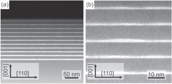
Figure 1. (a) HAADF STEM images of an 11-fold stack of GIB-QDs (light gray) separated by 15 nm thick Si spacer layers grown at 500 °C–600 °C (sample A). (b) Zoom-in revealing the flattened GIB-QDs.
Download figure:
Standard image High-resolution imageThe high TSi of 500 °C–600 °C has consequences on the shape of GIB-QDs. Sample capping at such high temperature causes segregation of Ge into the Si spacer layer. This leads to enhanced Si–Ge intermixing in the QDs [18–22] and in the wetting layer [22–25] between the QDs. The Si–Ge intermixing reduces the effective lattice mismatch between the GIB-QDs and the Si substrate causing flattening of the QDs [19]. This flattened GIB-QDs after Si spacer layer growth can be observed in figure 1. However, it is difficult to fully avoid Si–Ge segregation effects during sample capping, as they are present already at TSi = 350 °C [26] and increase with increasing TSi [19].
If TSi of the Si spacer layer is too low, complete breakdown of the epitaxial growth can arise during the formation of multilayer GIB-QD samples. Figures 2(a) and (b) show BF and HAADF STEM images of the multilayer GIB-QD sample B for which the Si spacer layer was grown at 350 °C–500 °C. Here, TSi is evidently at the limit below which a fully crystalline growth front cannot be maintained by SPER. Thus, while for some GIB-QDs SPER succeeded (blue arrow in figure 2(b)), it failed for others (yellow arrows in figures 2(a) and (b))3 . In figures 2(c)–(h), we schematically present the evolution of the large defect structure that can be observed in the STEM images in figures 2(a) and (b).
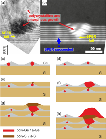
Figure 2. (a) BF STEM and (b) HAADF STEM image of a 10-fold multi-stack of GIB-QDs where the 12 nm thick Si spacer layers were deposited at 350 °C–500 °C (sample B). (c)–(h) Schematic evolution of the pronounced defect structure visible in (a) and (b). (c) QDs are partly amorphized by GIB. (d) Due to a too low TSi SPER is incomplete for one QD. (e) Growth of a polycrystalline/amorphous Si spacer on top of the non-crystallized GIB-QD. (f)–(h) Accumulation of Ge and Si at the defective crystal sites leading to a lateral and vertical expansion of the defect.
Download figure:
Standard image High-resolution imageAs a consequence of GIB, a part of the QD (gray color) is amorphised (red color), as depicted in figure 2(c). During Ge deposition and the subsequent ramp-down to TSi, the amorphous zones partly recrystallize (figure 2(d)). However, for TSi of 350 °C–500 °C not for all GIB-QDs recrystallization at the sample surface succeeds (figure 2(d)). At this non-crystalline surface the subsequently deposited Si spacer layer cannot grow epitaxially, i.e. it grows polycrystalline (poly-Si and poly-Ge) or continues to grow in an amorphous phase (a-Si and a-Ge). In the non-epitaxial regions, the strain caused by the Si–Ge lattice mismatch is lacking, which leads to Ge accumulation at this surface region during the deposition of the next QD-layer. In this way, the defect structure grows with increasing number of multilayers, as can be seen by the STEM images in figures 2(a) and (b).
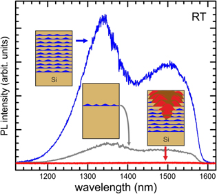
In figure 3, we summarize PL spectra of the multilayer samples, recorded at RT. As expected, for the multilayer sample for which the Si spacer layers were grown at too low temperature, no PL signal from the GIB-QDs is present (red spectrum in figure 3). Although there exist GIB-QDs for which SPER succeeded (see TEM image in figure 2(b)), it is evident that the breakdown of SPER in other, spatially separated regions, causes the formation of a large number of non-radiative recombination centers in the form of polycrystalline and amorphous Ge and Si regions. Hence, although the resolution of our PL setup is high with an excitation spot of ∼2 μm, we do not observe PL from those properly overgrown GIB-QDs because the carrier diffusion constants are very large in Si (on the order of cm2 s−1, [27]) and thus, the carriers are depleted by the abundance of non-radiative recombination centers in the regions where SPER broke down. This is not surprising in a system where it is known that the presence of a single dislocation can almost fully quench the PL emission from nearby, non-dislocated QDs [28, 29].
Figure 3. Room-temperature PL spectra from a single layer of GIB-QDs as used in [1] (gray) and from a 11-fold multi-stack (blue) for which TSi was 500 °C–600 °C. For the multi-stack sample for which the growth parameters were not optimized (TSi = 350 °C–500 °C), no PL signal was recorded (red).
Download figure:
Standard image High-resolution image
In contrast, for the same experimental conditions, strong PL from the multilayers of GIB-QDs is observed when the Si spacer layer growth parameters are optimized (blue-spectrum in figure 3). Notably, the PL-spectrum consists of two pronounced PL peaks, located around 1330 and 1520 nm. In [1] we have shown that such a double-peak structure is also present in single layer GIB-QD samples. For those, we have shown that the PL emission at shorter wavelength increases with increasing PL excitation power according to a power law of  with m = 1, whereas the emission at longer wavelengths increases with m = 0.6, which is usually associated with the presence of Auger recombination. Additionally, the PL-lifetimes of the emission at shorter wavelength is 2–3 orders of magnitude smaller than the ones of the emission at longer wavelength. In [1] we found that the activation energies for thermal quenching of the PL emission from the two peaks is the same (>300 meV) and thus very different from non-GIB, crystalline Ge QDs (∼60 meV). Thus, it is safe to assume that for both recombination paths leading to the two GIB-QD related peaks at 1330 and 1520 nm the electrons are strongly confined at the single defect site. Furthermore, in the supplementary information of [1] we have calculated ground and excited states for fully crystalline Ge-on-Si hut clusters using the nextnano3 program package [30, 31] and found that they are ∼100 meV apart. This is in excellent agreement with the energy splitting of the two PL peaks at 1330 and 1520 nm. Therefore, we tentatively ascribe the lower and higher energy PL peak to radiative transitions between electrons confined to the defect site and holes in the ground and first excited state of the crystalline part of the GIB-QD, respectively.
In order to fully verify this assignment of the two PL peaks, we will conduct in ongoing work PL investigations on GIB-QDs of larger size, such as pyramids or domes, where, due to smaller quantum confinement, the splitting between ground state and first excited state is significantly smaller.
To demonstrate the optical quality of the multilayer sample at RT, we compared its PL to the one of the single layer sample studied in [1], gray spectrum in figure 3. By forming microdisk resonators, we have observed lasing characteristics for this single layer sample [1]. Here we find that the PL signal from the multilayer sample is increased by a factor of 7.5 as compared to the single layer sample. Since the total thickness of the deposited epi-layer remained the same for the multi-layer GIB-QD sample as compared to the single layer GIB-QD sample, such multilayer samples are promising candidates for improved gain materials in single-mode group-IV nanophotonic laser devices in which the device thickness is limited to ∼200 nm. As a next step, we aim at the fabrication of photonic resonators containing the optimized GIB-QD multilayer samples described in this work.
Summary and conclusion
In summary, in this study we present a way to enhance the room-temperature PL properties of Ge ion bombarded QDs by vertical stacking. We stress that, due to the intrinsic formation procedure of the GIB-QDs, i.e. their initial partial amorphization, special care concerning the growth of the Si spacer layers has to be exercised. Their growth at low temperatures, ramped from 350 °C to 500 °C results in massive crystal defects that lead to full quenching of the GIB-QD PL. Optimized Si spacers, grown at temperatures ramped from 500 °C to 600 °C, lead to an PL intensity enhancement of about 650% as compared to single layer GIB-QD samples for which lasing was demonstrated.
Acknowledgments
We gratefully acknowledge the continuous support of A Rastelli, G Bauer and W Jantsch. This work was supported by the Austrian Science Funds (FWF): P29137-N36. HG acknowledges support of the European Commission under the H2020 grant TWINFUSYON (GA692034).
Footnotes
- 3
Note that due to an unwanted growth interrupt the thickness of the Si spacer layer between the second and third GIB-QD layer was reduced. However, breakdown of the epitaxial growth happened only after the growth of the fourth GIB-QD layer.