

Abstract
This study demonstrates the fabrication of uniform and vertically oriented SnO2 nanowires (NWs) using glancing angle deposition technique. The SnO2 NW was then subjected to different annealing temperatures of 350 °C, 550 °C, 650 °C, 750 °C and 900 °C in air, each for 1 h to discover the best optimized photodetector performance. The 650 °C sample showed the best photodetector material properties, with highest optical absorption, crystallinity, and reduced dislocation density. As such, the photodetector based on annealed 650 °C device exhibited an obvious best performance in terms of high responsivity as compared to other annealed samples. Also, a large UV responsivity of 2.58 A W−1 at 300 nm with high detectivity of 64.13 × 10¹⁰ Jones and a low noise equivalent power of 6.56 pW was observed for 650 °C sample. Thus, the increase in the crystallinity along with less scattering of photogenerated carriers enhanced the photoconductivity of 650 °C annealed UV photodetector.
Export citation and abstract BibTeX RIS
1. Introduction
One-dimensional (1D) metal oxide semiconductor nanostructures have attracted considerable interest in different areas like field-effect transistors, photosensors, lasers, detectors, gas sensors, and solar cells [1]. In the existing 1D nanostructures, metal oxide nanowires (NWs) exhibit excellent photodetection owing to its large surface to volume ratio, which strengthens the photon absorption process as well as the carrier separation capability. Among various metal oxide, SnO2, an n-type wide bandgap semiconductor (3.6 eV) material has attracted substantial attention for fabricating high-performance UV detectors due to its high optical, electrical and chemical stability [2]. Until now, a variety of deposition techniques such as atomic layer deposition (ALD) [3], vapor–liquid–solid (VLS) [4], electrospinning [5], chemical vapor deposition (CVD) [6], etc were reported depositing SnO2 NWs. But these fabrication methods involve complex processes and expensive equipment making it unsuitable for practical application. Therefore, fabrication of the high-performance photodetector (PD) using a simple and cost-effective technique is still challenging. Moreover, the presence of defects and dangling bonds in SnO2 plays a significant role in the photoconduction as well as photodetection process [7]. These defects act as a recombination centre which traps the photogenerated carriers thus reducing the photoconductivity and diminishing photodetection efficiency. Also, they act like donor impurities resulting in huge carrier concentration causing a higher dark current. Various reports on surface-related issues like oxygen adsorption and desorption process for different SnO2 nanostructures such as nano branch [8], nanotubes [9], ZnS/SnO2 [10] have already been reported. However, these nanostructure PDs have a common shortcoming of very low responsivity and detectivity along with higher carrier response time. Recently, the authors have reported photodetectors deposited using a cost-effective, catalytic free and well-controlled technique called glancing angle deposition technique (GLAD), a type of Physical Vapor Deposition (PVD) growth process [2]. However, due to the deficiency of oxygen inside the high vacuum chamber, a high number of defects are induced, especially in metal oxides using such type of PVD technique [11] limiting its overall photodetector performance. On such, post-deposition annealing in the air can be performed to change the surface chemistry by improving the crystal quality and reducing the oxygen vacancies. Moreover, the UV Photodetector response can be significantly enhanced by modifying the morphology, surface defects, and crystallinity of the metal oxides. The authors have recently shown a fast response UV detector based on the GLAD synthesized amorphous SnO2 NWs. But, the various device performance parameters such as responsivity, detectivity, etc need a significant improvement which can be achieved by modifying the surface or defects present in the SnO2 NWs. Various groups have explored the effect of annealing at different conditions on SnO2 material [1, 12, 13]. However, further study on modifications of defects after annealing in air is required to extract the optimized UV detector performance.
In this paper, SnO2 NWs deposited on the silicon substrate is reported using the GLAD technique and the influence of different annealing temperature on the structural, optical and electrical properties was investigated. The fabricated NWs were well aligned vertical structures which were confirmed by Field emission scanning electron microscope (FE-SEM) and transmission electron microscope (TEM) analysis. Thereafter, different parameters such as full width at half maximum of the diffraction peaks (FWHM), crystallite size, strain, and dislocation density were also computed for different annealed samples. Also, the UV response of the detector with the best-annealed sample was also explored. The results indicated that the properties of the GLAD deposited SnO2 NWs can be improved by annealing the sample to achieve the highest UV detector performance at an optimized temperature.
2. GLAD SnO2 NW fabrication method
GLAD technique was employed inside the e-beam chamber (BC-300, HHV INDIA) to synthesize SnO2 NW arrays on n-type 〈100〉 Si substrate. Prior to the deposition, the substrates were cleaned using the RCA process in an ultrasonication bath each for 3 min. Thereafter, SnO2 NWs were grown by evaporating the 99.999%, pure SnO2 material. The source and the substrates were placed at a distance of 24 cm inside the e-beam chamber with a base pressure of 5 × 10⁻⁶ mbar. The deposition was carried out at a constant growth rate of 0.12 nm s−1 to deposit 300 nm thickness for SnO2 NWs which was monitored using quartz crystal present inside the e-beam chamber. During the NW deposition, the substrate holder was tilted at an angle (85°) with respect to the source and also azimuthally rotated with a constant speed of 20 rpm. The samples were then annealed inside the muffle furnace (KL-1500X, MTI Corporation) at different temperatures of 350 °C, 550 °C, 650 °C, 750 °C, and 900 °C each for 1 h in air using even heating and cooling ramp of 6 °C min−1. Thereafter, the detectors were fabricated by depositing gold (Au) thin film (TF) of 30 nm thickness using a shadow mask with a circular hole of diameter 1.5 mm on top of SnO2 NWs which acted as a top electrode for the device.
2.1. Characterization
The fabricated samples were characterized using FE-SEM (Zeiss, Ultra 55), x-ray Diffraction (XRD) (Rigaku Ultima IV, CuKα radiation) and TEM with selected area electron diffraction (SAED) (JEOL JEM 2100) for studying the structural, compositional and morphological analysis. The optical characterization of the samples was carried out using UV–visible near-infrared (NIR) optical absorption spectrophotometer (Hitachi U-4100/UH-4150). The electrical characteristics of the device were measured using Keithley 4200-SCS along with a monochromator (Newport TLS-300XU) at room temperature.
3. Result and discussion
3.1. Morphological, optical and structural analysis
3.1.1. XRD analysis
Figure 1 shows the XRD analysis of SnO2 NWs measured at room temperature for different annealed samples at (350 °C, 550 °C, 650 °C, 750 °C, and 900 °C). The as-deposited GLAD SnO2 NWs was found to be amorphous in nature (not shown in figure 1) which was already reported by the authors recently in [11]. Thereafter, on annealing, the sample at 350 °C the sample still retain its amorphous behaviour, while on increasing the annealing temperature above it, the diffraction peak intensities become sharper. This may be due to defect healing and grain growth induced by annealing. All the SnO2 NW samples exhibited common diffraction peaks for SnO2 at angles of 2Ө = 26.5°, 33.9°, 37°, 51.6°, 66° which are assigned to (110), (101), (200), (211) and (301) planes respectively obtained from JCPDS (88-0287) for tetragonal structure. Also, a peak at 23.5° was obtained for SnO of orientation (111) for 350 °C, 550 °C, 750 °C, and 900 °C annealed samples from the JCPDS (24-1342). It is observed that the diffraction peak intensity is increased on annealing and is maximum at 650 °C. The increased intensity suggests better crystallization. Similar reports were also observed by various other researchers for different annealing temperatures [14–16]. Therefore, the crystallinity of the 650 °C is found to be better than all the other deposited samples. However, on increasing the annealing temperature beyond 650 °C, the intensity of the peak reduces. This may be due to the degradation of crystallinity as a consequence of variation in the grain boundary energy which made unusual growth of grains at higher annealed temperatures. Moreover, with higher annealing temperature, (900 °C) it is reported that an amorphous layer is generally formed (silicate layer) at the interface [1]. The presence of such an interfacial layer may be the reason for a reduction in the peak intensity at 900 °C [17]. Furthermore, from figure 1, it is seen that a small peak for SnO is observed in the case of 350 °C sample and which is reduced to a very small peak in case of 550 °C. On increasing the annealing temperature beyond 550 °C, the sample undergoes an oxidation process where the direct transformation of SnO to SnO2 phase occurs. However, in case of 650 °C, no peaks for SnO is observed which indicates a fully textured SnO2 film growth. But, on increasing the annealing temperature beyond 650 °C, the SnO2 phase destruction occurs and the SnO phase reappears. The SnO compound formation may also be due to the out-diffusion of oxygen into the silicon substrate to form an amorphous SiO layer at the bottom [18]. Also, the SnO2 degradation ratio (ISnO/ISnO2) was calculated and found to be 1.16 and 1.22 in case of annealed 750 °C and 900 °C sample, respectively which indicates higher degradation of SnO2 at higher annealing temperature.

Figure 1. XRD analysis of the SnO2 NW annealed samples.
Download figure:
Standard image High-resolution imageUsing XRD, various other important parameters like microstrain, dislocation density, stacking fault, etc can be calculated in order to understand the structural modifications that might have occurred after annealing at different temperatures. The microstrain value has been calculated using the equation [19],

The dislocation density (δ), represents the number of defects present in the crystal which is given by Williamson and Smallman's relation [19], δ = n/D2
where n is a factor equal to 1 providing minimum dislocation density and D is the grain size.
The effect of size and shape of the crystallite can be calculated using the Scherrer equation [19],  where k is the shape factor of 0.94, λ is the wavelength of the x-ray, β denotes the FWHM and D denotes the particle size. Thus, from figure 2(a) it can be seen that with the increase in the intensity of the peaks, the FWHM decreases whereas, the grain size is increased with a maximum at 650 °C. From figure 2(b), the microstrain and dislocation density is found to be least at 650 °C, which indicates that the concentration of lattice imperfections is reduced at this temperature. A higher microstrain indicates a high level of defects in the grain boundaries. Moreover, on annealing, local rearrangement of atoms in the grain boundaries occur for which the grain boundary defects and dislocation density is reduced and the overall microstrain is also reduced [20]. The stacking fault helps to determine the deformation mechanism and dislocation behaviour in the samples. It associates with the interruption of a normal stacking sequence of a crystal plane, which significantly influences the defects, dislocations, and deformation affecting the performance of the material under different annealing conditions [19]. It is denoted by,
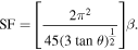

Figure 2. (a) Grain size and FWHM. (b) Dislocation density and Microstrain with respect to annealing temperature.
Download figure:
Standard image High-resolution imageOn plotting as shown in figure 2 it is seen that the stacking fault is least for 650 °C annealed sample which also verifies the lower concentration of lattice imperfections in this case.
Texture coefficient (TC) of a plane represents texture of a particular plane concerning the preferred crystal orientation which is given as,  where I(hikili) is the intensity of the diffraction peak of the sample, I0(hikili) is the intensity of the complete random sample and N is the number of diffraction peaks. TC > 1 indicates that the growth of the films has a higher degree of orientation to the 〈hkl〉 plane [16]. Thus, it is seen in figure 3 that the maximum TC value is obtained for 650 °C because the intensity of the peak is increased in this case which suggests the improvement of the crystal quality whereas it deteriorates for other annealed samples.
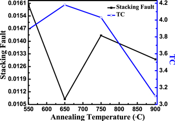
Figure 3. Variation of Stacking Fault and TC with respect to annealing temperature.
Download figure:
Standard image High-resolution imageTable 1 lists the various parameters of all the crystalline samples. From the table it can be concluded that the 650 °C sample gives the best crystallinity with minimum defect density as compared to all other samples.
Table 1. Comparison of the calculated parameters at various annealing temperatures.
| SL NO | Sample | 2θ | FWHM | Avg FWHM | Grain size (nm) | Avg. grain size (nm) | Dislocation density (δ) (×1015) (lines m−2) | Avg. dislocation density (δ) (×1015) (lines m−2) | Microstrain, ε × 10−3 | Avg microstrain, ε × 10−3 | Stacking fault | AvgStacking Fault | TC |
|---|---|---|---|---|---|---|---|---|---|---|---|---|---|
| 1. | 350 °C | — | — | — | — | — | — | ||||||
| 2. | 550 °C | 26.5 | 0.0456 | 0.036 | 3,26 | 4.9 | 94.09 | 59.43 | 11.08 | 8.56 | 0.024 | 0.0147 | 4.14 |
| 33.9 | 0.025 | 6.06 | 27.23 | 5.96 | 0.011 | ||||||||
| 51.6 | 0.038 | 4.19 | 56.96 | 8.63 | 0.014 | ||||||||
| 3. | 650 °C | 26.5 | 0.0319 | 0.024 | 4.67 | 6.78 | 45.8 | 26.92 | 7.75 | 5.73 | 0.016 | 0.011 | 4.18 |
| 33.9 | 0.0167 | 9.1 | 12 | 3.97 | 0.007 | ||||||||
| 51.6 | 0.0244 | 6.6 | 22.9 | 5.47 | 0.008 | ||||||||
| 4. | 750 °C | 26.5 | 0.0387 | 0.032 | 3.84 | 4.98 | 67.8 | 44.61 | 9.42 | 7.51 | 0.020 | 0.014 | 4.03 |
| 33.9 | 0.0249 | 6.08 | 27 | 5.95 | 0.011 | ||||||||
| 51.6 | 0.0318 | 5.04 | 39 | 7.17 | 0.014 | ||||||||
| 5. | 900 °C | 26.5 | 0.0324 | 0.029 | 4.59 | 5.32 | 47.4 | 36.47 | 7.88 | 6.86 | 0.016 | 0.013 | 3.14 |
| 33.9 | 0.026 | 5.82 | 29.5 | 6.21 | 0.012 | ||||||||
| 51.6 | 0.029 | 5.55 | 32.46 | 6.5 | 0.010 |
3.1.2. Optical absorption analysis
The optical absorption measurement was performed on the GLAD synthesized SnO2 NWs fabricated over quartz substrate for different annealed samples using UV–vis–NIR spectrophotometer. The absorption was carried out at room temperature under the wavelength range from 250 to 1000 nm as shown in figure 4. From the absorption graph, it is seen that all the samples absorb the maximum light in the UV region (250–400 nm) than in the visible region. Moreover, the absorption increases with annealing temperature and is highest in the case of the 650 °C sample. Thereafter, the absorption reduces with further increase in annealing temperature. The increased absorption in the case of the 650 °C annealed sample may be ascribed to the large generation of electron–hole pairs [21], improved crystallinity and higher grain sizes [22]. However, in the case of a 900 °C, 750 °C and 550 °C sample, absorption decreases due to the reduction in crystallinity and higher grain boundary defects (as observed from XRD) [21].
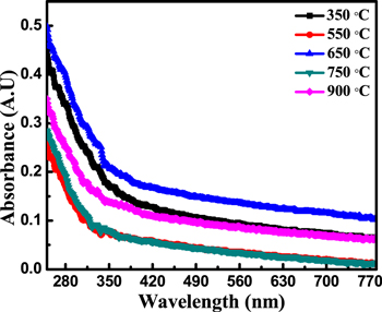
Figure 4. Absorbance spectrum of SnO2 NW annealed samples.
Download figure:
Standard image High-resolution image3.1.3. FE-SEM and TEM analysis of SnO2 NWs
Form the above analysis, it is observed that the 650 °C annealed sample showed the maximum improvement in the overall crystallinity among all the other annealed samples (350 °C, 550 °C, 750 °C and 900 °C) with reduced dislocation density and microstrain. Therefore, further investigation was carried out to understand its NW structural formation. Figure 5(a) shows the top-view image of the 650 °C annealed SnO2 NWs deposited on the n-Si substrate. The image shows that the NWs were grown with an average diameter and inter NW distance (separation between the NWs) of ∼27 nm and ∼40 nm respectively. Figure 5(b) shows the cross-sectional FE-SEM images of the 650 °C annealed SnO2 NW arrays. The image shows a uniform and vertically oriented SnO2 NWs fabricated over SnO2 TF/Si sample. The length of the NWs is calculated to be ∼185 nm and the thickness of SnO2 TF is found to be ∼30 nm. The uneven growth of SnO2 NWs (circle marked in both the figures) is due to the shadowing effect that is prevalent in the GLAD technique [11].

Figure 5. (a) Top-view and (b) cross-sectional view of annealed 650 °C SnO2 NWs.
Download figure:
Standard image High-resolution imageThe structural analysis of SnO2 NWs was also done using TEM analysis along with SAED for the annealed sample at 650 °C. Figure 6(a) shows the group of SnO2 NWs annealed at 650 °C. The magnified TEM image of a single NW is shown in figure 6(b). The length of the single NW is found to be ∼262 nm with a top diameter of ∼96.7 nm and a bottom diameter of ∼47.7 nm. Such an unsymmetrical pattern of GLAD NWs was also reported by the authors previously [2, 11]. The arrow in figure 6(b) indicates the growth direction. Moreover, the top inset shows the SAED patterns taken from the single NW signifies that the annealed 650 °C sample is polycrystalline in nature. The d-spacing measured from the magnified image (figure 2(b) (bottom inset), is found to be 0.34 nm which can also be verified from the XRD analysis. On calculation, using Bragg's law (from the XRD plot), the d-spacing is found to be ∼0.34 nm which is consistent with the above observation in TEM.

Figure 6. TEM Image of (a) group of SnO2 NWs annealed at 650 °C (b) Single SnO2 NWs annealed at 650 °C; top inset shows the SAED pattern and bottom inset shows the d-spacing.
Download figure:
Standard image High-resolution image3.2. Current (I)–voltage (V) characteristics
I–V characteristics of the fabricated device for different annealed temperature were measured at room temperature from +8 to −8 V under dark condition. Figure 7(a) shows the logarithmic plot of current (I) versus voltage (V) characteristics for all the annealed samples under dark condition. Figure 7(b) shows the schematic diagram of the device. The dark current value at −1 V for the annealed 350 °C, 550 °C, 650 °C, 750 °C, and 900 °C devices are found to be 2.37 μA, 0.9 μA, 26 nA, 2.59 μA and 1.42 nA respectively. It is observed that the dark current is lowest for 900 °C sample, which may be due to the formation of a parasitic layer (silicate layer) acting as a barrier to the current flow [1]. Thus, due to the presence of such interfacial layer, the 900 °C device may not be a good candidate for photonic devices. The next least dark current is observed for the 650 °C device other than 350 °C, 550 °C and 750 °C annealed devices. This is due to the good crystal quality of SnO2 NWs, with reduced defects, dislocation density and increase in the depletion width at the interface in comparison to other annealed samples. Moreover, the dark current observed for 650 °C was found to be lower than other recently reported SnO2 based photodetectors [11, 23, 24]. From the I–V graph, it is observed that the 350 °C device show a nonlinear rectifying behaviour indicating the formation of Schottky contact between Au and SnO2. However, in the case of a 650 °C sample, the rectification ratio (RR) (±8 V) is close to unity which signifies that the device behaviour changed from Schottky to near Ohmic characteristics. It is interesting to note that such ohmic behaviour is observed only for the 650 °C sample. Thereafter, with the increase in annealing temperature above 650 °C, the device again regains its Schottky behaviour. This change in the nonlinear behaviour of the I–V graph into the linear one in case of 650 °C sample, can be ascribed to the increase in the carrier concentration along with a reduction in the defect density at the interface [25, 26].
Figure 7. (a) Current–voltage curves of different annealed samples measured under dark condition (b) device schematic of the SnO2 NW based detector.
Download figure:
Standard image High-resolution imageThe current transport over the Schottky barrier can be known using the thermionic emission theory equation,  where I0 is the reverse saturation current, φB is the barrier height with device area of 1.77 × 10⁻² cm2, A* is the Richardson constant of value 120 A cm−2 K−2 [11]. On calculation, the barrier heights (BH) for annealed samples at different temperatures (350 °C, 550 °C, 650 °C, 750 °C and 900 °C) were found to be 0.75, 0.74, 0.63, 0.746, and 0.89 eV respectively. The highest reduction in BH is observed for the 650 °C annealed sample. This may be due to the reduction of grain boundaries as well as the scattering of carriers that occurred due to the reduction of defects [27] which are acting as a trapping site for the charge carriers. The lowest barrier may also be due to the ability of the charge carriers to cross the interface by increasing the surface carrier concentration that allows tunneling [25, 26] and as such near ohmic behaviour was observed in the case of 650 °C sample. Thus, the 650 °C sample show a near photoconductive effect whereas, a photovoltaic effect is observed in the case of the other annealed samples.
3.2.1. Photoresponse and switching
Upon white light illumination, the photoresponse (ILight/IDark) of the device increases in the reverse bias, depicting the Schottky diode characteristics. Figure 8 shows the variation of the photoresponse for voltage range −8 to 0 V (reverse bias) measured for the devices annealed at different temperatures 350 °C, 550 °C, 650 °C, 750 °C, and 900 °C. It is observed that the highest photoresponse is obtained for 650 °C annealed sample with a maximum value of ∼5 (at −8 V). This is due to the increased absorbance of the incident light which provides the generation of large number of electron–hole pairs in comparison to other annealed samples. The conversion to a near photoconductive mode makes the 650 °C device to contribute towards large photocarriers at the electrodes [11]. Another reason for such high value may be ascribed due to the improvement in the crystal quality and reduction in dislocation density which might increase the carrier concentration increasing the conductivity of the sample [24]. However, the photoresponse declines for the other annealed sample (350 °C, 550 °C, 750 °C and 900 °C) which may be due to the presence of bad crystallization and defects. However, in the case of the 650 °C device, the photoresponse increases linearly to the applied bias which signifies that the photocurrent can be tuned or controlled by varying the applied voltage at the electrode [27].
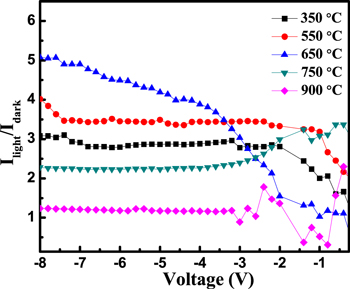
Figure 8. Photoresponse of all the SnO2 NW annealed devices.
Download figure:
Standard image High-resolution imageFigure 9(a) shows the on–off switching response for the annealed samples under regular interval of 20 s and at a fixed bias of −2 V. The rise time and fall time of the photocurrent were calculated by using the second ordered exponential fitting equations [2].
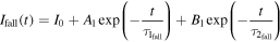
where I0 is the dark current, A1, A2, B1, B2 are constants and τ1rise, τ2rise, τ1fall, τ2fall are first-and second-time constants for rising and falling respectively.

Figure 9. (a) On–off Switching response of annealed 350 °C, 550 °C, 650 °C and 750 °C devices. (b) Rise time and (c) fall time with fitting curve for 650 °C annealed device.
Download figure:
Standard image High-resolution imageGenerally, two mechanisms are responsible for photoresponse in metal-oxide based photodetector. First, the generation and recombination of carriers related to the bulk given by τ1_rise and τ1_fall and secondly, the chemisorption process related to the surface given by τ2_rise and τ2_fall. Thus, on plotting the fitting graph as shown in figure 9(b), the rise time (τ2rise) for 350 °C, 550 °C, 650 °C, and 750 °C are found to be 0.185 s, 0.184 s, 0.183 s, and 0.189 s respectively. Also, the fall time (τ2fall) as shown in figure 9(c) are found to be 0.250 s, 0.251 s, 0.249 s, and 0.252 s for 350 °C, 550 °C, 650 °C, and 750 °C devices respectively. Moreover, equal rise (τ1rise) and fall time (τ1fall) of 2 ms is observed for 650 °C annealed sample which is much faster in comparison to the already reported as-deposited GLAD SnO2 sample [2]. Moreover, the photocurrent of all the annealed devices are almost consistent and repeatable, indicating that the devices are stable. However, in case of a 900 °C annealed sample, the presence of the silicate layer increases the barrier which therefore increases the resistivity of the device. Besides, the defects in the 900 °C sample acted as a recombination site which hindered the separation of the electron–hole pairs. Therefore, no switching response is observed in the case of a 900 °C annealed sample.
3.2.2. UV detector based on annealed SnO2 NW
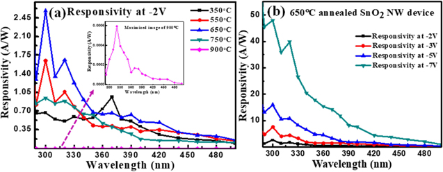
Figure 10(a) shows the spectral response of all the fabricated annealed photodetectors (350 °C, 550 °C, 650 °C, 750 °C and 900 °C (maximized as inset)) measured from 280 to 500 nm wavelength at −2 V applied bias (fixed at turn on voltage) figure 10. From the figure, it can be seen that the 650 °C annealed device shows higher responsivity as compared to the other annealed samples. Also, the 650 °C annealed device show a maximum peak responsivity of 2.58 A W−1 at ∼300 nm wavelength which may be ascribed to the band edge of SnO2. In addition, the annealed 650 °C device showed 18 times more enhancement in responsivity in comparison to the as-deposited SnO2 NW device, reported earlier by the authors [2]. As the 650 °C annealed sample showed improved crystallinity, reduced defects and dislocation density, and better responsivity, it can be concluded that the 650 °C annealed SnO2 material is more stable and efficient for the photodetector performance.
Figure 10. (a) Responsivity of all the annealed sample at −2 V, Inset shows the magnified image of the 900 °C annealed sample. (b) Spectral response of the annealed 650 °C at different applied bias.
Download figure:
Standard image High-resolution image
Further, the spectral response of the 650 °C annealed device is plotted as a function of various applied voltages in figure 10(b). On such, it is seen that the responsivity increases with the increase in the supply voltage since the photocurrent increases due to the efficient carrier collection. Thus, maximum responsivity of 2.58, 7.59, 15.97, 47.97 A W−1 is found for 650 °C annealed sample at different voltage of −2 V, −3 V, −5 V and −7 V respectively. The 650 °C device was further analysed to measure various important parameters such as detectivity and noise equivalent power (NEP).
Detectivity is an important parameter for characterizing the photodetector performance and it signifies to detect the smallest weak output signal which can be expressed as
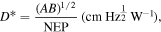
where D* is the detectivity, A is the effective area (1.77 × 10⁻² cm2), NEP is the Noise Equivalent Power and B is the bandwidth of 1 KHz [11] for the shot noise which is dominant noise for frequency below 1 KHz. The incident light power density is 18.19 μW cm−2 for 300 nm. By using the above equation, the detectivity is calculated and found to be 64.13 × 10¹⁰ Jones for 650 °C annealed sample at −2 V better than the as-deposited SnO2 NW reported previously by the authors [11]. The increased detectivity may be attributed to the reduction of defects which resulted in the better response of the sample in comparison to the as-deposited sample.
The authors have found their result to be better than some of the recently reported works as tabulated below in table 2. Moreover, various other device parameters such as external quantum efficiency (EQE) and UV–Visible rejection ratio were also calculated. The device showed a high EQE of 1.07 × 10³%, indicating that the adsorbed photon was able to activate a greater number of electron–hole pairs. The UV–Vis rejection ratio (R300/R480) was found to 11.77 at −2 V indicating that the device is more sensitive to UV light and therefore can be potentially used as a visible-blind photodetector. However, more improvement is required which can be obtained by designing various nano-heterostructure using SnO2 NWs.
Table 2. Comparison table for different UV-PDs.
| SL NO | Material | Wavelength (nm) | Responsivity (mA W−1) | Detectivity (Jones) | NEP (W) | tr (s) | tf (s) | Year | Reference |
|---|---|---|---|---|---|---|---|---|---|
| 1. | InTiZnO | 290 | 170 (10 V) | — | — | 88.6 | 2.1 | 2018 | [28] |
| 3. | MgNiO MSM | 320 | 17.8 (5 V) | 1.5 × 10⁹ | 2 × 10⁻¹⁰ | — | — | 2019 | [29] |
| 4. | ZnO TF, MSM | 370 | 0.44 (3 V) | — | — | 4.17 | 11.0 | 2019 | [30] |
| 5. | SnO2 NT | 320 | — | — | 5 | 15 | 2018 | [9] | |
| 6. | Zn1−xPxO TF | 365 | 180 (0.01 V) | 2.6 × 10¹⁰ | — | 2019 | [19] | ||
| 7. | Zn0.98Fe0.02O/ZnO TF | 365 | 1560 (0.01 V) | 6.45 × 10⁹ | — | 73 | 42 | 2018 | [31] |
| 8. | Sn doped Ga2O3 TF | 254 | 36.1 (50 V) | — | — | 0.94 | 1.37 | 2017 | [32] |
| 9. | Au/SnO2 NW (as-deposited) | 370 | 143 (−2 V) | 10.8 × 10¹⁰ | 38.8 × 10⁻¹² | 0.18 | 0.25 | 2019 | [11] |
| 10. | Annealed Au/SnO2 NW | 300 | 2580 (−2 V) | 64.13 × 10¹⁰ | 6.56 × 10⁻¹² | 0.002 | 0.002 | (this work) |
4. Conclusion
In summary, vertically aligned SnO2 NWs were successfully synthesized using GLAD technique. Thereafter, structural, optical and electrical performance of the samples were investigated and compared as a function for the different annealing temperatures of 350 °C, 550 °C, 650 °C, 750 °C, and 900 °C. The improvement in the crystallinity from amorphous to polycrystalline in nature was observed from XRD analysis with a maximum crystallinity at 650 °C. An enhanced optical absorption was also observed for 650 °C sample due to increase in grain size and generation of large electron–hole pairs. The 650 °C SAED analysis also showed polycrystalline SnO2 NW which was consistent with the XRD analysis. The resulting photodetectors fabricated with all annealed samples showed an obvious higher photodetector performance with the 650 °C annealed sample among all. The reduction in defect along with an accumulation of higher charge carriers resulted in a better response for the 650 °C sample. In addition, the UV detector with 650 °C as compared to other annealed devices, showed a maximum responsivity of 2.58 A W−1 at 300 nm with corresponding detectivity of 64.13 × 10¹⁰ Jones and a low NEP of 6.56 pW. Thus, these results showed that the SnO2 NW can be used as a potential candidate for high-performance UV photodetectors device by optimized air annealing.