

Abstract
The tungsten oxide (WOx) thin films have been deposited by a novel hot filament oxidation-sublimation process and applied in the dopant-free heterojunction solar cells as the hole selective contacts. The oxygen flow ratio plays a significant role during the deposition process. With increasing the oxygen flow ratio from 1.7% to 6.7%, the morphology of WOx films changes from small cauliflower-like particles to large cluster accumulation, and the ratio of W6+ increases from 76.1% to 91.4% with the ratio of W5+ decreasing from 23.9% to 8.6%. The work function of WOx can be tailored in a range of 5.5–6.1 eV by increasing the oxygen flow ratio. Its optical band gap maintains above 3.2 eV with the conductivity of about 10−5 S·cm−1. We have applied the WOx films in dopant-free silicon heterojunction solar cells as the hole selective contact layer by replacing the p-type amorphous silicon layer. By taking advantage of the highly transparent WOx layer, a high photon-current density of 39.6 mA·cm−2 was achieved with the oxygen flow ratio of 1.7%. It is interesting to find that the optimum cell conversion efficiencies of 14.9% were obtained with the oxygen flow ratio of 1.7% and the thickness of 10–20 nm for the deposition of WOx layer. This work proves the feasibility and good potential of Hot-Wire CVD prepared WOx hole selective contact for efficient dopant-free silicon heterojunction solar cells.
Export citation and abstract BibTeX RIS
1. Introduction
The parasitic absorption of the p-type or n-type doped amorphous silicon layers in silicon heterojunction solar cells limits the further increase of photon generated current density [1, 2]. The dopant-free passivating contacts are of highly scientific and technical interest for silicon heterojunction solar cells due to their reduced parasitic absorption, as well as ease-of-deposition [3, 4]. Metal oxides and fluorides of low work function (WF) such as lithium fluoride [5], magnesium fluoride [6], tin oxide [7], and niobium oxide [8], are the candidates for electron selective contacts. On the other hand transition metal oxide of high WF like molybdenum oxide (MoOx ) [9–11], tungsten oxide (WOx ) [12, 13], vanadium oxide [14, 15] can be the candidates for hole selective contacts. The hole-selective contact is often used as the window layer, where materials of both wide bandgap and high WF is on the top in the candidate list. So far a cell conversion efficiency of 23.5% with MoOx hole selective contact has been reported [9]. Yet the evaporated MoOx tends to be unstable under elevated temperature during the subsequent processes of metallization and post annealing [16, 17]. Amongst the reported hole-selective contacts, WOx has the largest optical band gap and can remain stable with the processing temperature up to 200 °C [18–20].
The stoichiometry value x of WOx is crucial for its opto-electrical property influencing the cell performance [21]. Several deposition techniques have been reported for the preparation of WOx films including magnetron sputtering, vacuum thermal vapor deposition [20, 22–24]. It is difficult to tune the composition of WOx using thermal vapor deposition. Magnetron sputtering causes sputtering damage to the WOx /Si interface [25]. Known as ion bombardment free and conformal deposition, the Hot-Wire chemical vapor deposition (HWCVD) is a relatively mild deposition process and the composition of the deposited film can be adjusted by adjusting the gas flow rate. Some literature has reported the use of similar deposition methods and studied the structure of as-deposited WOx and tried to apply it in electrochemistry [26–28]. However, less attention has been paid to the effect on their opto-electrical properties. So far there are few reports on the WOx thin films prepared by HWCVD for solar cells as the hole selective contact.
In this study, the WOx films were prepared by a novel hot filament oxidation-sublimation process in a high-vacuum chamber. The oxygen flow ratio has been varied to moderate the material property of WOx films. The composition, surface morphology and opto-electrical properties of these films were investigated. These WOx hole selective layers were applied in dopant-free silicon heterojunction solar cells, resulting in high photon current densities of 39.6 mA·cm−2 and conversion efficiencies of 14.9%.
2. Experimental details
All WOx films were deposited by direct oxidation of the tungsten wire in a HWCVD chamber. The purity of the tungsten wire is 99.99%, and the wire diameter is 0.5 mm. Five straight tungsten wires were arranged in parallel with a length of about 22 cm. The distance between the tungsten wire and the substrate is about 8 cm. A gas mixture of oxygen and argon was adopted as the deposition gases. The oxygen flow ratio rO2, as defined as the flow rate of oxygen (fO2) divided by total flow rate (fO2 + fAr), namely rO2 = fO2/(fO2 + fAr), was varied in a range of 1.7%–6.7%. The total flow rate was kept at 80 sccm. The working pressure was 5 Pa. The hot wire current is 48 A, leading to an estimated filament temperature of about 1600 °C. All WOx samples were co-deposited on glass and silver coated glass substrates at room substrate temperature. The sample on silver coated glass substrate was used for the Raman measurement (Thermo Scientific, USA) with the excitation laser wavelength of 473 nm. The film thickness was measured by a step profiler (Brucker DektakXT). The surface topography was measured by scanning electron microscopy (SEM, ZEISS EV0 MA15). The root-mean-square (RMS) roughness and surface potential of WOx thin films were measured using atomic force microscopy (AFM, KEYSIGHT Technologies 7500) via tapping mode. The surface potential was determined by the contact potential difference between the Pt-coated conductive cantilever probe and the samples. The WF of the sample can be calculated. Further details on the calculation of the WF can be found elsewhere [11]. The optical transmittance of WOx films was measured by a UV–VIS–NIR spectrophotometer (SHIMADZU UV-3600 Plus). The composition of samples was measured by the x-ray photoelectron spectroscopy (XPS, Thermo Fisher ESCALAB XI+). The sample surface was etched using clusters with an etching energy of 4 keV for 50 s. All core level spectra were calibrated using the C1s (284.8 eV) peak. The conductivity of WOx films on a glass substrate was measured at room temperature with two silver pads in parallel.
The WOx films prepared by HWCVD were applied in silicon heterojunction solar cells as the hole selective contact. The schematic drawing of the cell configuration and its photo are shown in figure 1. The solar cell area is about 4 cm2. The n-type silicon wafer based structure of a-Si:H(i)/n-c-Si/a-Si:H(i)/a-Si:H(n+) was adopted. The wafers were soaked in hydrofluoric acid solution for 3 min before deposition. We tested the implied Voc for WOx /a-Si:H(i)/n-Si contact with the Photoconductance Lifetime Tester (WCT-120, USA). The indium tin oxide film with a thickness of about 90 nm were prepared by magnetron sputtering. On top of the WOx layer, the 100 nm-thick indium zinc oxide (IZO) films were prepared by sputtering. The cell was finished with silver contacts, and then annealed at 120 °C in air for 30 min. The current–voltage performance of the solar cells was measured with a sun simulator (WAVELABS Sinus-220, Germany) under standard conditions. The external quantum efficiency (EQE) of the solar cell was measured at room temperature.
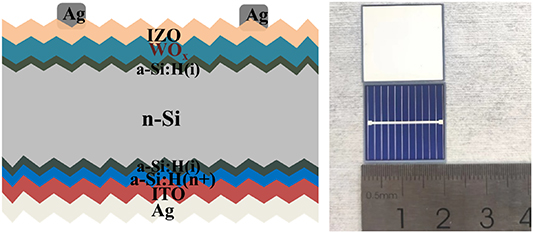
Figure 1. Schematic drawing of the silicon heterojunction solar cells with WOx hole selective contact and the photo image of the front and back of the solar cell.
Download figure:
Standard image High-resolution image3. Results and discussion
3.1. Material property of WOx thin films
Figure 2 shows the deposition rate of WOx films with the oxygen flow ratio rO2 ranging from 1.7% to 6.7%. The film thickness of all samples is about 150 nm. The deposition rate increases linearly from about 5 nm·min−1 at rO2 = 1.7% to 50 nm·min−1 at rO2 = 6.7%, which indicates that high oxygen concentration favors for the growth of WOx .
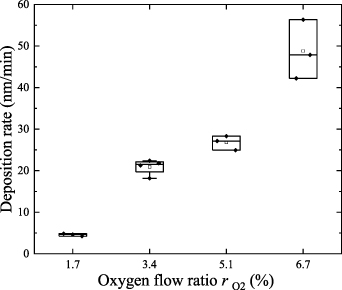
Figure 2. Deposition rate of WOx films with different oxygen flow ratio rO2 = 1.7%–6.7%.
Download figure:
Standard image High-resolution imageFigure 3 shows the Raman spectra of WOx films deposited with different rO2. The Raman signals in the wavenumber region of 200–450 cm−1 can be assigned to the bending vibrations of O–W–O bond vibration modes [29]. A peak band in the wavenumber range of 550–1000 cm−1 can be observed. The peak centered at 714 cm−1 and 804 cm−1 can be assigned to the asymmetric and symmetric stretching vibrations of W6+−O bond, respectively, corresponding to the WO3 phase [30]. These two signals tend to enhance with increasing oxygen flow, indicating the increasing of WO3 composition. A peak centered at around 950 cm−1 could be the stretching mode of unsaturated W=O bond [29], and it shifts to lower wavenumbers at higher rO2. One could argue that this is due to the stoichiometric value x increases.

Figure 3. Raman spectra of WOx films deposited with different oxygen flow ratio rO2 = 1.7–6.7%.
Download figure:
Standard image High-resolution imageThe RMS roughness of these WOx films measured by AFM increases generally from about 6.1 nm to 15.2 nm by increasing the rO2. Figure 4 shows the SEM images of the corresponding WOx samples. It is shown that small cauliflower-like clusters on the surface at rO2 = 1.7% and the diameter of the clusters is about 50 nm. When the rO2 increases to 3.4%, the cluster diameter increases to about 100 nm and the gap between clusters increases. As the rO2 increases further to 5.1% and 6.7%, a number of larger clusters with the diameter over 200 nm seem to accumulate. This could be correlated with the high deposition rates, where the abundant WOx particles combine in the gas phase prior to the deposition on the substrate. It is noted that the room substate temperature was applied. The largely combined particles may not integrate sufficiently on the substrate. Hence the films prepared at high oxygen flow ratio tend to show higher porosity [31].

Figure 4. SEM images of tungsten oxide films with different oxygen flow ratio rO2 = 1.7%–6.7% (a) rO2 = 1.7%. (b) rO2 = 3.4%. (c) rO2 = 5.1%. (d) rO2 = 6.7%.
Download figure:
Standard image High-resolution imageFigure 5 shows the XPS signal of the W4f core level of the WOx samples with rO2 = 1.7%–6.7%. The main peaks at the binding energies of 36.0 eV and 38.1 eV are attributed to the W6+ 4f7/2 and 4 f5/2, respectively. The additional shoulder at 34.8 eV can be the W5+ 4f7/2, which is paired with the W5+4f5/2 at 37.0 eV [20, 32, 33]. The presence of W5+ in all four samples indicates the existence of non-stoichiometric WOx and possible oxygen vacancy. The W 4 f signal was deconvoluted as indicated by the dashed line in figure 5 for the calculation of W6+ and W5+ content ratio. When rO2 = 1.7%, the W6+ ratio is 76.1%. As the rO2 increases the W6+ ratio increases to 91.4%, while the W5+ ratio decreases. This is in agreement with the weakening of the Raman signal at 950 cm−1 as shown in figure 3.
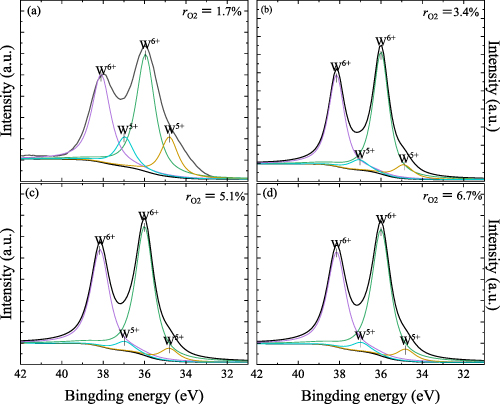
Figure 5. W4f core level XPS signals of WOx films deposited with oxygen flow ratio rO2 = 1.7%–6.7% (a) rO2 = 1.7%; (b) rO2 = 3.4%; (c) rO2 = 5.1%; (d) rO2 = 6.7%.
Download figure:
Standard image High-resolution imageAs shown in figure 6(a), the surface potential (SP) of the WOx film decreases from −0.5 V to about −1.1 V, as the oxygen percentage increases from 1.7% to 6.7%. The WF of these WOx samples were calculated given the surface potential measured by Kelvin probe force microscopy (KPFM) [11]. The WF of the samples increases from about 5.5 eV to 6.1 eV with rO2 increasing from 1.7% to 6.7%. The higher WF could be mainly caused by the more oxygen content [24, 34].

Figure 6. Surface potential (a) and work function (b) of WOx films as a function of different oxygen flow ratio rO2 = 1.7%–6.7%.
Download figure:
Standard image High-resolution imageThe transmittance of WOx thin films on the glass substrate are included in figure 7(a). We used air as the test baseline. The transmittance of WOx /glass is higher than 80% in the wavelength range of 370–1200 nm. The optical bandgap Etauc of these WOx samples were evaluated using the Tauc plot model [35]. It is shown in figure 7(b) that all samples are highly transparent with Etauc above 3.2 eV. By increasing the rO2, the Etauc increases slightly by about 0.1 eV. This could by mainly due to the increases stoichiometry value as indicated by the XPS and Raman results.
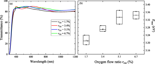
Figure 7. Transmittance (a) and optical band gap Etauc (b) of WOx films as a function of different oxygen flow ratio rO2 = 1.7%–6.7%.
Download figure:
Standard image High-resolution imageThe conductivity of these WOx samples is in the order of 10−5 S·cm−1 as shown in figure 8. The conductivity of the WOx films prepared by HWCVD was about 2.1 × 10⁻⁵ S·cm−1 when rO2 = 1.7%. The conductivity decreases by half when the rO2 increases to 6.7%.
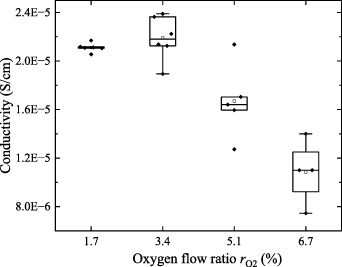
Figure 8. Conductivity of WOx films as a function of different oxygen flow ratio rO2 = 1.7%–6.7%.
Download figure:
Standard image High-resolution image3.2. Dopant-free heterojunction solar cells with WOx
The WOx films deposited with oxygen flow ratio rO2 = 1.7%–6.7% are used as the hole selective contact layer in dopant free silicon heterojunction solar cells. Given the deposition rate in figure 2 the thickness of WOx hole selective contact is about 15 nm by controlling the deposition time. Figure 9 shows the current–voltage (JV) parameters of these solar cells with WOx hole selective contact. As the rO2 increases from 1.7% to 6.7%, the short-circuit current density (JSC) increases from 37.5 mA·cm−2 to nearly 38.0 mA·cm−2. This is due to that the higher optical band gap with increasing rO2. The implied open circuit voltage (VOC) of WOx films with different oxygen flow ratio rO2 was tested on the silicon wafer. We found that the implied VOC of all samples lightly increases from 694 mV to 699 mV with increasing the oxygen flow ratio. Yet the measured VOC shows a significant decrease from about 640 mV to 550 mV with increasing rO2. This is similar to what has been reported in other literatures, in which the VOC of cells with either MoOx or WOx hole-selective transport layers decreases with increasing oxygen flow ratio [24, 36]. Such decrease of VOC could be related to contact interface, band alignment with the transparent conductive oxide contact, and material quality. The FF decreases from 63% to about 45% with increasing rO2. One of the reasons can be the lower conductivity of the WOx layer, which leads to higher series resistance. As a result, the cell conversion efficiency (η) decreases from about 14.0% to about 10.0% with an increasing rO2.
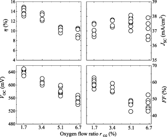
Figure 9. Dependency of current–voltage parameters of solar cells including conversion efficiency (η), open circuit voltage (VOC), short-circuit current density (Jsc) and fill factor (FF) on the oxygen flow ratio rO2 = 1.7%–6.7%.
Download figure:
Standard image High-resolution imageFigure 10 shows (JV) parameters of cells as a function of WOx layer thicknesses (5–30 nm). The oxygen flow ratio was 1.7% for this cell series. As the WOx film thickness is less than 10 nm, the cell suffers from low JV parameters like JSC = 37.0 mA·cm−2, VOC = 560 mV and FF = 53%. This is mainly due to the poor band bending when the hole selective contact is too thin. Additionally, the following sputtered IZO layer could cause a decrease in the WF of WOx thin films, leading to the deterioration of hole selective transport in WOx thin films [25, 35]. As the WOx film thickness in the range of 10–20 nm, both JSC and VOC tend to maintain at 37.5 mA·cm−2 and 640 mV, respectively, despite of a certain scattering in the data. While the FF shows a slight decrease from 63% to 55%. The JV parameters deteriorates severely as the WOx film thickness increases further above 25 nm. Overall, the optimum WOx film thickness is in the range of 10–20 nm as taking the cell conversion efficiency into account.
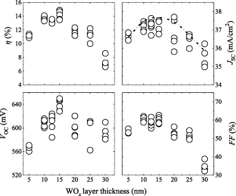
Figure 10. Dependency of current–voltage parameters of solar cells including conversion efficiency (η), open circuit voltage (VOC), short-circuit current density (Jsc) and fill factor (FF) on the WOx thickness (5–30 nm).
Download figure:
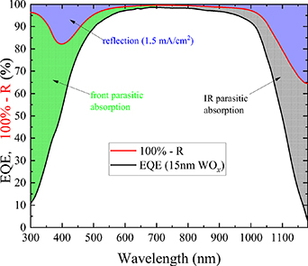
Standard image High-resolution imageFigure 11 shows the EQE of the best cell shown with 15 nm-thick WOx hole selective contact as well as the reflection on the cell surface. In the 500–1000 nm wavelength range the average EQE of the cell reaches 96.6%. The optical losses of the best device is analyzed using the EQE and 100%-R data, as proposed by Holman et al [37]. The evaluated photon current density JQE by EQE is about 39.6 mA·cm−2 and the integrated current density of the reflected light is about 1.5 mA·cm−2. Considering the wide bandgap (>3.0 eV) of WOx and IZO films on the front side of the solar cell [38], it is suggested that the parasitic absorption is mainly caused by the intrinsic amorphous silicon passivation layer in the 300–600 nm band. The current loss of the backside is caused by the poor reflection effect of the non-mirrored rear silver contact [14].
Figure 11. External quantum efficiency (EQE) and surface reflection of the solar cell with 15 nm-thick WOx layer prepared with oxygen flow ratio rO2 = 1.7%.
Download figure:
Standard image High-resolution image
4. Conclusions
The deposition of WOx films by the HWCVD technique with oxygen flow ratio rO2 range of 1.7%–6.7% was investigated. The opto-electronical properties of WOx films were analyzed in correlation with the material composition and structure. The WOx films with WF of 5.5–6.1 eV, the conductivity of 10−5–10−6 S·cm−1, and the optical band gap of 3.2–3.4 eV were obtained. These WOx layers were applied in dopant free silicon heterojunction solar cells as the hole selective layer. Thanks to the highly transparent WOx layer, a high photon current density of 39.6 mA·cm−2 in EQE measurement was achieved. It is found that the optimum cell efficiency of 14.9% was obtained with the WOx layer thickness of 10–20 nm and low oxygen flow ratio rO2 = 1.7%. Despite of the high oxygen flow ratio favoring the formation of stoichiometric WOx , our study shows that the solar cell JV parameters especially open circuit voltage and fill factor deteriorates at higher oxygen flow ratio. The poor interface between the intrinsic passivation layer and the WOx contact could be the main cause. One might improve the interface property by adjusting the filament temperature or substrate temperature. Nevertheless, this work shows the feasibility of WOx hole selective contact by HWCVD for silicon heterojunction solar cells and good potential for its industrial application.
Acknowledgments
This work is supported by the National Natural Science Foundation of China (Nos. 51702269 and 61904154), Innovation Research Team Project of Southwest Petroleum University (No. 2019CXTD10), Sichuan Science and Technology Program (No. 2022YFG0229), Chengdu Science and Technology Project (Nos. 2022-YF05-00384-SN and 2020-GH02-00014-HZ). The authors would like to thank Xianhui Cui, Yan Xiang and Haichuan Zhang for their assistance with the measurements.
Data availability statement
All data that support the findings of this study are included within the article (and any supplementary files).