

Abstract
The development and application of second generation high temperature superconducting (2G-HTS) tapes have attracted much attention in China recently. Progress in upscaling high performance 2G-HTS tape production at Shanghai Superconductor Technology (SST) is reported in this paper. With ion beam assisted deposition, biaxially textured buffer layers with a configuration of CeO2/LaMnO3/MgO/Y2O3/Al2O3/C-276 have successfully been fabricated. In-plane and out-of-plane texture degrees of CeO2 films achieve 2°–4° and 2°, respectively. A multi-plume multi-turn pulsed laser deposition (PLD) system combined with the so-called 'radiation assisted conductive heater' has been proposed and further developed for REBCO layer deposition. Our effort was focused on minimizing the temperature variations in the deposition region by modifying the heating shield that assists the conductive heater of the drum-like cylinder. A tape travelling speed of 100–180 m h−1 can be achieved with a steady temperature profile when passing through the deposition zone, which is very beneficial for the growth of the REBCO layer. Taking advantage of the liquid phase growth mode, several compositions of superconducting films with a thickness in the range of 1–2.5 μm have been grown with high growth rates of over 40 nm s−1. Furthermore, the microstructures and superconducting performance were investigated in detail. Based on these studies, superconducting tapes with piece lengths of up to 500 meters have been developed. High Ic values at 77 K, self-field (over 520 A cm−1 width) or at low temperature, high magnetic field conditions (over 560 A/4 mm width at 4.2 K, 10 T, perpendicular field) have been achieved. Lamination and jointing techniques have also been developed by SST for power and magnet applications.
Export citation and abstract BibTeX RIS
1. Introduction
In recent years, increasing numbers of universities, research institutes and companies including power utilities in China are carrying out research with superconductors for energy generation, storage and transfer. Second generation high temperature superconducting (2G-HTS) tapes are considered one of the most promising practical superconductors that can be used in power and magnet applications. For typical applications, even just prototypes, several hundreds of kilometers of high performance and long length 2G-HTS tapes are usually needed. However, to date there are only a few companies worldwide with an annual throughput of over 300 kilometers (4 mm wide tape) [1–3]. With the financial support of Chinese central and local government, as well as the input of strategic investors, a 2G-HTS industry circle is forming in the Yangtze River Delta region in China. Three companies, Shanghai Superconductor Technology (SST), Shanghai Creative Superconductor and Suzhou Advanced Materials Research Institute, have been established with the goal of commercializing 2G-HTS tapes, using pulsed laser deposition (PLD) [4], metal–organic decomposition [5] and metal–organic chemical vapor deposition [6], respectively.
SST, a young and vibrant company established in 2011, is a spin-off from Shanghai Jiao Tong University. The aim of SST is to offer high performance 2G-HTS wires at low cost, not only for domestic consumption and related national projects, but also worldwide with customized specifications. After more than five years of R&D, two types of 2G-HTS tapes have been successfully developed for 77 K, self-field and low temperature, high magnetic field applications and commercialized since 2015. In this paper, we are providing for the first time an overview of the fabrication processes and quality control of 2G-HTS tapes at SST. We shall also discuss the multi-plume multi-turn PLD system with a 'radiation assisted conductive heater' for high growth rate superconducting layer deposition. Finally, we will discuss the lamination and jointing techniques for practical applications.
2. Fabrication techniques and characterizations
2.1. Fabrication of 2G-HTS tapes
The structural configuration of 2G-HTS tapes fabricated at SST is shown in figure 1, which is a typical ion beam assisted deposition (IBAD) + PLD layered structure. 10 mm wide, 50 μm thick C-276 Hastelloy tape is used as the substrate. Prior to film deposition, the Hastelloy tapes are first put through an electropolishing process to achieve an Rs of about 1 nm within a 1 μm by 1 μm region (measured by atomic force microscopy). A stack of buffer layers with the architecture of CeO2/LaMnO3/MgO/YO3 is deposited. The layer composition and deposition techniques are indicated in figure 1. All of the oxide buffer layers are fabricated in a reel-to-reel manner with a tape travelling speed of about 70–400 m h−1. The throughput of such a textured template is over 300 km/year for 10 mm wide tapes. Superconducting layers with various compositions are deposited by using a multi-plume multi-turn PLD system with a KrF excimer laser (LAMBDA 300 K). In our R&D process, optimization of the heating system for the large deposition area was performed in order to minimize temperature variation on the tape passing through the deposition zone. The details of this process and heating cylinder will be discussed in the following section. During deposition the oxygen partial pressure was set to be 300–500 mTorr (depending on the compositions of the targets), and the laser energy in the chamber was between 500–700 mJ with the repetition rate of the laser pulse being about 260–280 Hz. A superconducting layer with a thickness in the range from 1.5–2.5 μm can be fabricated by repeating the deposition two to four times. For power and magnet applications, three REBCO compositions were adopted, where GdBa2Cu3O7 is used for 77 K, self-field applications, and the other two compositions are EuBCO +BaHfO3 and YGdBCO phases (denoted as compositions A and B, respectively, hereafter), both being used for low temperature and high magnetic field applications. Lastly, a silver layer of 1–2 μm and a copper layer of 5–20 μm (depending on the user's requirement) are deposited by sputtering and electroplating techniques, respectively.
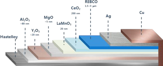
Figure 1. Architecture of 2G-HTS tape developed at SST, where the Al2O3, Y2O3 and LaMnO3 layers are deposited by sputtering, the MgO layer by IBAD, the CeO2 and REBCO by PLD.
Download figure:
Standard image High-resolution image2.2. Characterization of structural and superconducting properties
The microstructure of the oxide buffer layers and superconducting layers are routinely characterized by optical microscopy, atomic force microscopy and x-ray diffraction analysis. A reel-to-reel accessory has been developed and installed in the x-ray diffractometer with an area detector, allowing it to scan and analyze the phase and texture of a short sample continuously. Due to the high reliability of the buffer layer stack fabrication process, routine quality control is carried out only on both ends of each tape. During IBAD-MgO layer deposition, an in situ reflected high energy electron diffraction (RHEED) detector is used to monitor the texture quality at the surface of the MgO layer. For short superconducting samples, Ic at 77 K, self-field was measured by the conventional DC four-probe method with the criterion of 1 μV cm−1. Low temperature in-field Ic values were calculated based on the Bean model from the magnetization results, or obtained through direct conventional DC four-probe measurements. Longitudinal Ic distribution over long REBCO tape is measured by an MCorderTM based on the inductive method [7]. For such inductive measurement, Ic values at both ends of the long tape were calibrated using four-probe measurement. Transmission electron microscopy (TEM) observations of the sample's cross section were performed using a Tecnai G2 F20 S-Twin operating at 200 kV.
3. Results and discussions
3.1. Buffer layer architecture and characterization
The IBAD-MgO process is crucial for buffer layer fabrication. The surface texture of IBAD-MgO is very sensitive and plays an important role in the texture formation of the final cap layer. Figure 2 shows the RHEED patterns of the IBAD-MgO layer along a one kilometer-long tape, where the sharp patterns are obtained at the MgO surface. This result demonstrates the high stability of SST's IBAD process with the high tape traveling speed of 100 m h−1. However, even with the sharp RHEED patterns observed, we found that CeO2 (111) texture sometimes forms when directly deposited on the IBAD-MgO layers. With insertion of the RF-sputtered LaMnO3 (LMO) layer prior to the CeO2 layer, this issue has been resolved. Figure 3 shows the texture quality comparisons of the PLD-CeO2 layer with and without the LMO layer among several batches of tapes produced. Evidently, the texture component in the CeO2 layer with the LMO layer turns to single CeO2 (002) orientation, i.e., the undesirable secondary texture component CeO2 (111) disappeared. It is well known that CeO2 (111) is fatal for further epitaxial growth of the REBCO layer and can result in a Jc reduction of more than 50% in our case. More interestingly, the out-of-plane texture also becomes sharper, while the in-plane texture remains unchanged. Considering that all the CeO2 layers were deposited under the same conditions to the same thickness, the so-called 'self-epitaxy' effect [8] of the CeO2 layer is principally the same as observed on the IBAD-MgO and on the sputtered LMO. So we deduced that the texture improvement is likely to be related to the stress releases or minor defect coverage by the LMO layer. The in-plane and out-of-plane texture degrees of the PLD-CeO2 layers are routinely found to be 2°–4° and 2°, respectively, whilst the roughness is around 2 nm, as per atomic force microscope measurements.

Figure 2. RHEED patterns collected along the long IBAD-MgO tape.
Download figure:
Standard image High-resolution image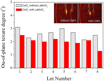
Figure 3. Out-of-plane texture degree of CeO2 films with and without insertion of the LaMnO3 layer, and the inset shows the 2D XRD patterns collected on the two typical CeO2 films.
Download figure:
Standard image High-resolution image3.2. Radiation assisted conductive heating system for deposition of the superconducting layers
Deposition temperature is one of the most crucial parameters for the PLD process. It is challenging to measure and analyze the practical deposition temperature when the tape is travelling, especially with high density plumes. Researchers from Bruker HTS and from Fujikura have proposed their solutions in their heating systems, i.e., quasi-equilibrium heater [9] and hot-wall heater [10, 11], respectively. In our PLD, a drum-type heating system is adopted in order to realize the large deposition zone with high travelling speeds. In such a system, the tape is wound on the steel cylinder turn by turn as described in our previous publication [12]. A schematic side view of the heater is shown in the top right corner of figure 4. The deposition zone is at the bottom part of the cylinder. The tape starts to be heated prior to touching, or when touching, the cylinder. As soon as the tape comes out from the right shield, REBCO begins to be deposited on the tape surface. The projection of the deposition zone can be approximated as a rectangle, i.e., the two sides of the rectangle are equivalent in length to the axial and azimuth directions of the cylinder, the area of which is related to the lane number and the arc of the cylinder exposed to the plumes. Herein, we studied the temperature variation along the arc of the cylinder, which is associated with the heating process and tape traveling speed. In our study, we noticed that the shields next to the heating cylinder have a significant effect on the tape temperature variation. Three factors—the geometry of the heating shield, the distance between the shield and the cylinder, as well as the tape travelling speed—have been taken into thorough consideration. In this study, we mainly optimize the geometry of the heating shield while maintaining high tape traveling speed. Figure 4 shows the temperature profiles measured on a tape with a high travelling speed of over 100 m h−1 before and after optimization. Obviously, within the deposition zone the temperature variation is no greater than 10 °C, which is a remarkable improvement. It is believed that the improved temperature homogeneity is beneficial for the formation of thicker films and films with composite structure.
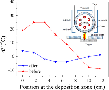
Figure 4. Temperature variation of the running tape passing through the deposition zone (before and after optimization of the heating shields), and the inset is the schematic side view of the heater.
Download figure:
Standard image High-resolution image3.3. Superconductivity of the 2G-HTS tapes for power and magnet applications
Optimized deposition parameters are applied for the fabrication of long length REBCO tapes. By repeating the deposition (two to four times), film thicknesses in the range of 1–2.5 μm, depending on the Ic requirements of the users, can be achieved. We have selected GdBa2Cu3O7 targets for 77 K, self-field applications. The longitudinal Ic distribution of a 300 meter piece of GdBa2Cu3O7 tape is shown in figure 5. The average Ic is over 520 A cm−1 width with standard deviation of less than 2%. The minimum and maximum Ic values are 504 A and 544 A, respectively. High Ic homogeneity can also be observed on a 4 mm wide tape after slitting. The local Ic drops (indicated by arrows in figure 5) observed are related to the defects on the metallic substrate. We have also investigated the target compositions (A and B) on the Ic(B) properties in the REBCO films, as shown in figure 6. Typically, we achieve Ic values of over 280 A/4 mm width at 30 K, 5 T and over 560 A/4 mm width at 4.2 K, 10 T (magnetic field being perpendicular to tape surface) in our production line. Anisotropy values of γ in the REBCO are around 2 (determined by the Blatter scaling approach [13–15]), which is much smaller than that for pristine YBCO (γ = 5 ∼ 7) [16, 17]. Through the XRD analysis, we did not observed nanorods along the c-axis in the REBCO films. Cross sectional TEM observation was performed, as shown in figure 6. It reveals a large amount of stacking faults instead of particles or column-like structures. This observation is further confirmed by the angular dependence of in-field critical current measurements shown in the inset of figure 7. A sharp Jc/ (θ) peak appears when the external magnetic field is parallel to the ab plane. This is attributed to both intrinsic pinning [18, 19] and extrinsic planar defects parallel to the ab-planes such as stacking faults [20, 21]. It is known that partial dislocations always form at the boundary between the stacking faults and REBCO matrix [22, 23]. Such defects could act as effective point pinning centers when the magnetic field is away from the ab-planes [24]. In particular, short length stacking faults increase density of the dislocations, leading to larger internal strains in our case. Therefore, the Ic anisotropy and in-field performance could be dramatically improved. One should notice that both films were deposited with the high growth rate (over 40 nm s−1). Such microstructural characteristics might be strongly associated with the liquid phase during deposition, which needs to be studied further.
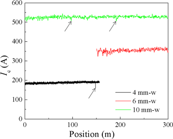
Figure 5. Ic distribution along the tapes with various widths.
Download figure:
Standard image High-resolution image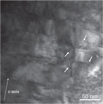
Figure 6. TEM cross sectional observation of the REBCO film with enhanced superconductivity at magnetic fields, where the arrows point to the stacking faults.
Download figure:
Standard image High-resolution image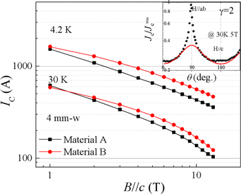
Figure 7. Ic as a function of external magnetic fields at 30 K. The inset shows the Ic (θ) behaviors at 30 K, 5T, where the scattered dots represent the data measured by the four-probe transport method, and the red curve is fitted using the Blatter scaling approach (γ = 2).
Download figure:
Standard image High-resolution image3.4. Lamination and jointing techniques of the superconducting tape
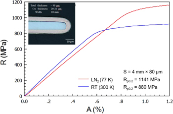
Besides superconductivity and Ic uniformity, lamination as well as the jointing techniques have also been extensively studied. Based on advanced lamination techniques [25], various lamination materials including stainless steel, brass, and copper can be used in order to fulfill different application requirements. Among them, one should notice that copper stabilized tape has the highest yield stress of over 1000 MPa at liquid nitrogen temperature, while the Ic retention is higher than 95% at a bending diameter of 5 mm (when the REBCO layer is facing inward). This data is comparable to other published data when 20–30 μm thick Hastelloy substrate is used in the 2G-HTS tapes [26]. The smaller critical bending diameter in our case is associated with the unique deposition conditions, as described previously. Namely, the REBCO layer in the tape is 'naturally' under compressive strain in the straight condition. Moreover, the 'dog-bone' defect of copper-plating has been overcome by shielding during the electroplating process. As shown in the inset of figure 8, the thickness nonuniformity of the copper layer is less than 10%. An overcurrent of 1200 A (in 100 ms) can be applied at 77 K on the tape with stainless steel lamination, while the room temperature resistance is also adjustable by optimizing the thickness combination of the stainless steel and copper stabilizer. Table 1 lists SST's existing jointing techniques and the characteristics, some of which have been published [27–29].
Figure 8. Tensile test of the copper-plated tape at room temperature and at liquid nitrogen temperature, and the inset shows the cross section at the edge of the copper-plated tape.
Download figure:
Standard image High-resolution image
Table 1. Joint techniques developed at SST, and their characteristics.
| Type | Characteristics | Resistance | Note |
|---|---|---|---|
| Hand soldered | Fast and convenient | 25 nΩ cm2 | Commercialized |
| 1st generation low-resistance joint [27, 28] | Automated production; highly robust | 2–150 nΩ | Commercialized |
| 2nd generation low-resistance joint [29] | Low resistivity; potential for higher Je | 1–3 nΩ | Technical support |
4. Conclusion
In this paper, we have summarized the recent progress by SST in the development of 2G-HTS tape. High quality IBAD-MgO metallic substrates were successfully fabricated, and in-plane and out-of-plane texture degrees of 2°–4° and 2°, respectively, were achieved in CeO2 films. We have also invested a great deal of effort in the optimization of deposition conditions for the multi-plume multi-turn PLD process. The temperature variation in the deposition zone was extensively studied. A so-called 'radiation assisted conductive heating' system was proposed. As a result, the temperature uniformity is significantly improved along the tape when passing through the deposition zone. Moreover, taking advantage of the liquid assisted growth mode, a high growth rate of over 40 nm s−1 is achieved for the REBCO films, which is beneficial to the increase of throughput of the production line. Under optimized deposition conditions, high 77 K, self-field and in-field Ic values can be achieved by using various compositions of superconducting targets. Analyses of structural and superconducting properties also confirm that enhancement of low temperature, in-field Ic is mainly attributed to noncorrelated defects, such as stacking faults and dislocations, which can also effectively act as pinning centers for minimizing the intrinsic anisotropy. For practical power and magnet applications, SST has also developed lamination and jointing techniques. Improved electromechanical performance and low joint resistance were achieved.
Acknowledgments
The authors would like to acknowledge the financial support from National Key Research and Development Program 2017YFB0902301 and National Natural Science Foundation of China (51502171), and the author Yue Zhao would like to acknowledge the Program for Professor of Special Appointment (Eastern Scholar) at Shanghai Institutions of Higher Learning.