

Abstract
For next-generation accelerator magnets for fields beyond those achievable using Nb–Ti, Nb3Sn is the most viable superconductor. The high luminosity upgrade for the Large Hadron Collider (HL-LHC) marks an important milestone as it will be the first project where Nb3Sn magnets will be installed in an accelerator. Nb3Sn is a brittle intermetallic, so magnet coils are typically wound from composite strands containing ductile precursors before heat treating the wire components to form Nb3Sn. However, some mechanical assembly is still required after the coils have been heat-treated. In this paper, we present direct evidence of cracking of the brittle Nb3Sn filaments in a prototype dipole that resulted in degraded magnet performance. The cracking of the Nb3Sn, in this case, can be attributed to an issue with the collaring process that is required in the assembly of dipole accelerator magnets. Metallographic procedures were developed to visualize cracks present in the cables, along with quantitative image analysis for location-based crack analysis. We show that the stresses experienced in the damaged coil are above the critical damage stress of Nb3Sn conductor, as evidenced by a measured Cu stabilizer hardness of 85 HV0.1, which is higher than the Cu stabilizer hardness in a reference Nb3Sn cable ten-stack that was subjected to a 210 MPa transverse compression. We also show that once the collaring procedure issue was rectified in a subsequent dipole, the Nb3Sn filaments were found to be undamaged, and the Cu stabilizer hardness values were reduced to the expected levels. This paper provides a post-mortem verification pathway to analyze the damage, provides strand level mechanical properties, which could be beneficial for improving model prediction capabilities. This method could be applied beyond Nb3Sn magnets to composite designs involving high work hardening materials.
Export citation and abstract BibTeX RIS
1. Introduction
Nb3Sn is the most viable conductor for high field accelerator magnets in the range of 10–16 T for High Energy Physics research [1]. Beyond the Large Hadron Collider (LHC) the next generation Future Circular Collider (FCC), a 100 TeV hadron-hadron collider, is expected to use both Nb3Sn dipoles and quadrupoles operating at 16 T, 4.2 K [2]. Challenges involved in the construction of 16 T Nb3Sn magnets include the development of production quality conductors that can carry a demanding current density, Jc, of 1500 A mm−2 (16 T, 4.2 K) and magnet designs incorporating stress management to control the high stresses experienced by Nb3Sn conductors during magnet construction and under the influence of Lorentz forces during operation. Recently achieved increases in the upper limits of Jc in Nb3Sn strand indicate that sufficiently high Jc to meet FCC requirements is now possible [3, 4]. Furthermore, an experimental prototype Nb3Sn dipole magnet has recently generated the significant milestone field of 14 T. Further design testing is now underway for a 15 T target field, where conductor degradation in high-stress regions is a major concern [5].
A crucial step in the development of high field Nb3Sn magnets is the major upgrade of the LHC, called High Luminosity LHC (HL-LHC). Tens of Nb–Ti magnets will be replaced with Nb3Sn dipole and quadrupole magnets using state-of-the-art Nb3Sn conductor. The 11 T dipole magnets [6] are the first Nb3Sn magnets that will be installed in a particle accelerator. They will provide the same integrated field as the standard 8.3 T LHC dipoles over a shorter length, which allows the installation of additional collimators in the LHC arcs.
Stress management is a critical issue in Nb3Sn magnets due to the brittle Nb3Sn phase. Although the conductors are wound and then reacted to minimize mechanical stresses on the Nb3Sn filaments, there remain several avenues leading to conductor damage. Improper assembly may result in overstressing and coil damage, thermal expansion mismatch of the coil, and magnet constituents can cause damage during thermal cycling, Lorentz forces generated during powering may overstrain the Nb3Sn. FE simulations can provide useful but approximate predictions of the stress distribution in the magnet during the different assembly and operational conditions; however, the prediction of precise stress levels remains a challenge.
During cold testing of an 11 T dipole short model magnet at CERN, a critical current limitation of the coils was detected. It was suspected that the reason for this degradation was fracturing of some of the Nb3Sn filaments as a result of excessive mechanical stress during the collaring of the coils. A post-mortem (destructive post magnet testing) metallographic analysis technique has been developed in order to provide more in-depth insight, at the conductor level, into the degradation and complexity in stress states. This approach was previously demonstrated in Nb3Sn cable-in-conduit magnet sections tested for the ITER project [7–9].
This paper provides a roadmap for different aspects related to damage and microstructure in Nb3Sn model dipole coils. A comparison between multi-axial loaded dipole sections versus uniaxially loaded cable ten-stack sample sections indicate variations in the damage behavior. A technique to resolve the effects of stresses on the filament level using Cu microhardness measurements s presented in this paper. This technique could be applied to future model magnets and also provide granular data to provide realistic stress values for the development of stress prediction models for complicated magnet assemblies.
2. Experimental methods
For the current study, we have analyzed two 11 T dipole coil cross sections, which were rough-cut using a band saw after disassembling the magnets after cold testing and then precision cut with a diamond wire saw. The coil cross-section and the coil collaring procedure are discussed in detail in [10]. 11 T dipole cable ten-stack samples [11] were also evaluated. Figures 1(a)–(e), provides a visualization of the dipole section at various stages of disassembly. An 11 T dipole collared aperture containing two coils is shown in figure 1(a). Figure 1(b) shows a photograph of the short model coil #109 after magnet cold test and disassembly. The dipole design used in the 11 T dipole magnet is indicated in the top view of the solid model in figure 1(c). The sectional view (Section AA) in figure 1(d) shows the various components that make up the dipole segment, including (a) Nb3Sn cables, (b) austenitic stainless steel 316L loading plate which presses against the loading pole, (c) oxide dispersed Cu (DISCUP 30®) wedges. The insulating layers and epoxy impregnation that is present in the dipole cross-section are not indicated in the figure here. The 11 T dipole Nb3Sn coils are segmented into six different conductor blocks, as numbered in figure 1(d). To evaluate metallographic details of cross-sections, different dipole coil sections were cut as shown in figure 1(e). The orientation of the samples polished from the dipole section corresponded to the plane containing the axial and transverse directions. The nomenclature of the sections consists of the conductor block number following the word section, and the corresponding row cut from the section. As indicated in figure 1(e). Section 1-R1, shows the section from coil block #1, the first row cut from coil block #1 indicated by R1. The two-layer Nb3Sn segments in the cross-sections are indicated as Row 1–9, with each row consisting of two Nb3Sn conductor segments.

Figure 1. Segments of the 11 T dipole coil at various stages of disassembly, (a) cross section of collared 11 T dipole coil assembly made of two coils, (b) 11 T dipole short model coil #109, (c) top view of a 11 T dipole coil, (d) cross-sectional view of section AA, including the cut dipole segment of Coil #109 used in this study, (e) isometric view of the dipole section to visualize the coil segments analyzed by metallography.
Download figure:
Standard image High-resolution image2.1. Details of 11 T dipole coils for this study
For this metallographic study, two coils were selected for analysis, short model coil #109, which showed severe critical current degradation, and 11 T dipole series coil GE-C02 that did not show current degradation.
After collaring coil #109 was assembled in 11 T twin aperture dipole MBHDP102, as shown in figure 1(a). Cold tests of MBHDP102 revealed a substantial critical current limitation at the mid-plane turns of coil #109, and the n-value was also strongly suppressed [10, 12], both indications of possible Nb3Sn filament breakage. The critical current limitation probably caused the relatively low quench currents of magnet MBHDP102.
The critical current deterioration, which was detected over an extended length in the straight part of the coil, was presumed due to excessive mechanical stresses applied during the collaring of the coil [10]. Section AA in figure 1(c) is a coil cross-section in which filament damage is expected. Coil #109 was de-collared and central section cuts were made for metallographic examination. A central section is shown in figure 1(d) was diamond wire saw cut and analyzed further.
The second coil investigated here (GE-C02) was the second series 11 T dipole coil collared in the 11 T dipole aperture HCMBH_C001-01000001. There was a difference between manufacturing procedures used in GE-C02 versus coil #109. The series coil GE-C02 has an optimized insulation scheme, and the collaring procedure was improved to reduce the mechanical stress on the Nb3Sn conductor during collaring. Finite element simulations of the stress distribution in the coil during the Collaring procedure indicate that the highest stresses are experienced at the coil midplane on the Nb3Sn cables in section 1-R1 [13].
The aperture, including coil GE-C02, was cold tested in a 'hybrid' magnet assembly where the second aperture was not powered. Powering tests after the first magnet cool down showed excellent quench performance, and in particular, no critical current degradation at the coil mid-plane was observed. However, after an additional thermal cycle, the coil performance was degraded, due to a critical current (Ic ) limitation at the coil ends (making the magnet available for destructive post-mortem analysis). The degradation at the coil ends was presumably caused by warming the magnet too fast. For metallographic examination, the coil samples were extracted in the central- straight part of GE-C02 (similar to the coil section in #109). In the central section of GE-C02, no filament damage is expected [10].
2.2. Description of 11 T dipole cable ten-stack samples
The ten-stack samples are made of ten 11 T dipole cables (nominal width and mid-thickness are 14.7 mm and 1.25 mm, respectively [14]), which are stacked alternatingly in order to compensate for the keystone angle of 0.79°. The Rutherford cables are made of 40 Restacked-Rod Process type Nb3Sn strands with 0.7 mm nominal diameter, which were produced by Oxford Instruments Superconducting Technology (now Bruker-OST). The Rutherford cables have a 25 μm thick stainless steel core, and they are surrounded by a 0.15 mm thick cable insulation made of mica tape and S2/E-glass fiber. The Nb3Sn formation heat treatment was performed with a ramp rate of 50 °C h−1 and was comprised of three isothermal plateaus of 210 °C-48 h, 400 °C-48 h and 665 °C-75 h. The ten-stack samples are designed to be comparable to dipole cable sections; the wire volume in the ten-stack samples that were analyzed is 72%. The Cu in this sample is assumed to be fully annealed after the prior heat treatment to a peak temperature of 665 °C. More information about the ten-stack sample production and mechanical loading has been published in [15].
Ten-stack samples No 28 and No 33 (figure 2) were uniaxially loaded to compressive peak stress of 210 MPa. Ten-stack #28 was loaded in the transverse direction (corresponds to figure 1(e)), and No. 33 was loaded in the axial direction. Unloaded sample #57 was used as a reference in this study.

Figure 2. Ten-stack Nb3Sn coils in three different states: (a) #28-compression loaded to 210 MPa (change to 210 MPa in the figure) along the direction transverse to the Nb3Sn wire cross-section, (b) #33-compression loaded to 210 MPa along the axis of the superconductor wire, and c) is an unloaded ten-stack.
Download figure:
Standard image High-resolution imageComposite theory predicts iso-strain in the composite constituents under axial loading [16]. This has been confirmed experimentally for the Nb3Sn filaments and Cu matrix in different Nb3Sn wires by high energy synchrotron x-ray diffraction [16], and in ten-stack samples by neutron diffraction [8]. At 210 MPa (sample 28), the macroscopic axial ten-stack stresses in the Nb3Sn and Cu are about 450 MPa and 100 MPa, respectively [17].
Transverse loading theory predicts iso-stress [18] in the composite constituent materials [19]. Neutron diffraction measurements confirm that under transverse macroscopic ten-stack stress of 210 MPa (sample 33), the stress in the Nb3Sn filaments and in the Cu matrix is very similar and correspond to the externally applied stress of 210 MPa [11].
2.3. Metallography
For metallographic evaluation, the samples were mounted in a clear epoxy-hardener mixture, which was cured at room temperature (RT). Subsequent sectioning was performed using a wafering saw with the sample glued to a base plate to avoid the danger of damage that might be caused by clamping the sample directly. The samples were mechanically polished using SiC pads with a decreasing grit size of 320, 400, 600, 800, and 1200. The load on the sample during the grinding process was 12 N, and the cross-sectional area of the mount was ~500 mm2. After the grinding process, the samples were polished using diamond slurries of successively decreasing particle size (5 µm, 3 µm, 1 µm). The final polishing step used a 50 nm colloidal silica solution with a pH ~ 11 in a Vibromet® vibratory polisher. This polishing procedure is a standard metallographic sample preparation technique; however, the low loads are essential here to maintain the integrity of the sample. The samples were lightly etched in a 1:1: HF:H2O solution for 10 min to make the cracks more visible by light microscopy. In order to remove staining from the etch, the samples were returned to the vibratory polisher for 30–45 min, after which the samples were cleaned and dried for further imaging.
Imaging of the cracks was performed using an Olympus BX41M reflected light microscope combined with an Olympus UC50 digital camera and Olympus Stream capture software. Backscattered Electron (BSE) images were obtained using a Zeiss ESB- FESEM. Analysis of shape and crack density was performed using FIJI-ImageJ [20, 21], combined with custom routines for superconductor analysis [8].
Vickers microhardness tests were performed on the polished cross-sections of the dipole and ten-stack samples using a LECO 300 AT hardness tester. The load dependence on the hardness was verified over the complete range of 10 g–1 kg on the unloaded ten-stack samples. For hardness comparisons, a 100 g load with a dwell time of 15 s was used in this study. The hardness measurements are designated HV0.1 XX, where HV signifies Hardness Vickers (scale), and the subscript 0.1, means the applied load in kg, and XX is the hardness number derived from the diagonal indent measurements.
Metallography and hardness measurements in this paper focus on section 1-R1 in dipole coils #109, and GE-C02, where the stresses on the Nb3Sn cables are predicted to be maximum from available simulation results [13]. A complete description of the metallographic process development and comparisons between different coil sections are underway and will be presented elsewhere.
3. Results
3.1. Nb3Sn crack distribution in coil #109
Section 1-R1 of Coil #109 was mounted, polished, etched, and imaged. Cracks were observed in this section with varying densities based on location. Crack morphologies vary in the filament, as shown in figure 3. The commonly found cracks are angular. There are also many curved cracks and a few cracks that have a wavy or crushed appearance. The Cu surrounding the filaments indicate deformation contrast, as observed by the mottled appearance of Cu in figure 3. The cracks that are observed were counted in each Nb3Sn sub-element in the high-stress section 1-R1. The number of cracks varies between 10 and 1000 depending on location in the section. Some cracks show a strong correlation to the porosity in the Nb3Sn filament. The shape of the cracks also varies from angular to curved cracks. Crack density spatially varies, as shown in figure 4. There were cracks observed in Section 2 as well (not shown here). However, the crack numbers tapered in other sections and will be a part of a subsequent paper.

Figure 3. FESEM-BSE image of polished and etched high stress region in model coil #109 at the interface between two strands shows cracks in the Nb3Sn filaments. The crack morphologies vary depending on location in this section with possibility of—angular oriented cracks, curbed cracks and wavy cracks. The adjacent Cu also reveals diffraction contours related to strain in the BSE image.
Download figure:
Standard image High-resolution image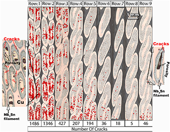
Figure 4. Light micrographs of section 1-R1 showing local variations in the number of cracks within the section. Some of the cracks are correlated to porosity. The crack orientations also vary between angular and curved cracks possibly indicating the state of stress in the Nb3Sn filaments.
Download figure:
Standard image High-resolution imageHere was no Ic degradation in coil GE-C02 after training. There were no cracks detected in this analyzed coil. A representative BSE image of Row 1 is shown in figure 5, and it can be seen that the Cu matrix in the core of the strand contains annealing twins, typical of recrystallized Cu. Nevertheless, deformation contrast is observed in Cu along the edges of the superconductor wire.

Figure 5. FESEM-BSE image of a polished and etched high stress region in model coil GE-C02 shows no evidence of cracks in the Nb3Sn filaments. Annealing twins are observed in the Cu matrix.
Download figure:
Standard image High-resolution image3.2. Nb3Sn cracks in ten-stack samples after uniaxial compression to 210 MPa in transverse and axial directions
Ten-stack samples were uniaxially compressed in transverse versus axial directions to a similar stress value of ~210 MPa. Figure 6 shows that sample #28, which was loaded in the transverse direction, has Nb3Sn cracks along the sub-element filament major axis. The Cu stabilizer shows signs of deformation contrast, as indicated by the BSE image. In contrast, the axially compressed ten-stack sample #33 does not show any cracks in the Nb3Sn. Figure 7 shows a typical wire cross-section, with regions around the wire edges where deformation contrast in Cu is observed even in the axially compressed samples.

Figure 6. Cross-sectional FESEM-BSE image of transverse compression sample #28 which underwent a stress of 210 MPa, reveals straight cracks that run through the Nb3Sn sub-elements. The plane being imaged here is the Transverse- Axial plane.
Download figure:
Standard image High-resolution image
Figure 7. Cross-sectional BSE image of axial compression sample #33, indicates no cracks the Nb3Sn sub-elements. The plane imaged here is the Radial- Transverse plane.
Download figure:
Standard image High-resolution image3.3. Cu microhardness on ten-stack samples #28, 33, 57, and dipole coil cross-sections #109 and GE-C02
The strain contrast observed in Cu in various samples indicates permanent plastic deformation in Cu. In order to verify if there are changes in the microhardness of the Cu in the different sections, microhardness tests were conducted on the Cu regions in the center of the wires in all the samples. There were differences in the hardness of Cu between samples, as shown in figure 8. From the undeformed ten-stack sample #57 we can see that the hardness of Cu, which is in the annealed condition after the 650 °C/50 h Nb3Sn heat treatment, is about HV0.1 37–50. The hardness increases as the stress are applied on the ten-stack. Sample #33, which had been subjected to axial compression of 210 MPa, has a hardness between HV0.1 45 and 53, and the transversely loaded 210 MPa compression sample #28, has hardness values between HV0.1 62 and 75. The scatter in the data could be as a result of inhomogeneous deformation in different sections.

Figure 8. Vickers hardness variation in the Cu stabilizer for the different samples in this study. The dipole segment hardness for model coil #109 varies between a low of 55 to a high of 80.
Download figure:
Standard image High-resolution imageA comparison between the Cu hardness in coils #109 and GE-C02 indicates that the hardness variations in #109 are high and in the range between HV0.1 52 and 80, whereas in C02 the hardness values overall are lower, ranging between HV0.1 45 and 60. In order to further evaluate hardness in the model coil, we investigated the hardness of Cu in each row of the high-stress section as indicated by the plot of hardness versus rows in figure 9. We observe that the distribution of hardness as a function of rows in #109 is highest for Row 1, and Row 2, with several points beyond the HV0.1 65, the highest hardness measured in the section #109 is ~80 in Row#1, and the lowest hardness is about 55 in Row #9. There are several points that are over HV0.1, that are distributed along the rows in #109. There is a general trend of decreasing hardness from Row 1 through to Row 9. For a similar section in Coil GE-C02, figure 10 indicates a general lower overall hardness compared to coil #109. The lowest hardness in Cu occurred in Row 3, and Row 8 and corresponded to values as low as HV0.1 ~ 35. The highest hardness was around HV0.1 62 and occurred in Row 8 of the section.
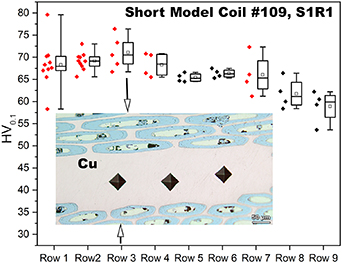
Figure 9. Vickers hardness distribution in the Cu along the different rows of coil #109 section S1R1. Hardness measurements made in the Cu adjacent to filaments with cracks are marked in red.
Download figure:
Standard image High-resolution image
Figure 10. Vickers hardness along the different rows of the 11 T series dipole coil GE-C02 cross section.
Download figure:
Standard image High-resolution image
In summary, we observe that there are cracks found in short model coil #109, and 210 MPa transverse loaded ten-stack sample #28. The hardness measured on Cu in regions where the Nb3Sn filaments are cracked overall higher, and there are regions where the hardness values are beyond HV0.1 70, with the highest values measured around HV0.1 80. In coil GE-C02, and ten-stack sample A33 compressed to 210 MPa axially where metallographic examinations do not show any cracks in the cross-section has an overall lower hardness with lesser scatter in the Cu wire centers.
4. Discussion
Magnet coils are mechanically loaded: (a) at ambient temperatures during magnet assembly, especially during collaring, (b) during thermal cycling due to the presence of constrained components with varying thermal expansion coefficients, and (c) due to Lorentz forces during powering. Our results confirm that short model coil #109 was degraded due to the formation of Nb3Sn cracks, presumably due to overloading stress at RT during collaring, and as expected, no Nb3Sn cracks were found in the straight part of the 11 T dipole series coil GE-C02. We discuss the details of the results which support this analysis.
4.1. Crack formation in Nb3Sn cables at RT for 11 T dipole samples
The results that we report here indicate that the 11 T dipole coils have been subjected to a multi-axial stress state. This is indicated by the Nb3Sn crack distribution and the varying crack orientations shown in figure 3. Observed cracks are curved and angular meaning complex loading conditions that lead to differences in principal stress directions. Cracks are oriented along principal planes and in principal directions in the ten-stack sample A28, which is transversely loaded to 210 MPa. The transverse compressive stress limit of the 11 T dipole Rutherford cable has been determined by critical current measurements after transverse compressive loading the cable at RT. It was observed that when the transverse compressive stress exceeds about 150 MPa a significant critical current degradation occurs [22]. Lorentz force simulations of the 11 T dipole indicate that the main region for high stress is around 145 MPa ([13], figure 5.25, pg. 59) in section 1-R1, however, figure 4 indicates that there is extensive damage in regions in #109 away from the high stresses caused by the Lorentz forces. The absence of cracks in the same high-stress region in coil GE-C02, which consists of a similar design and volume fraction of epoxy and cable indicates that the stress during the training or magnet operation does not cause this damage. The degradation of coil GE-C02 that was detected in the coil end after the thermal cycle of the magnet is presumably caused by stresses due to thermal expansion mismatch. The samples analyzed in the straight section did not fail, there was no Ic degradation, and as expected, we do not observe cracks in the Nb3Sn filaments.
4.2. Cu hardness as an indicator of material state in the 11 T dipole magnet
Cu hardness values in the different samples indicate that Cu hardness variations can reveal the stress distribution to which the coil was submitted at the conductor level. For annealed polycrystalline Cu, the expected hardness is HV0.1 45–50 and increases with work-hardening as the Cu gets strained [23–25]. The present results of undeformed ten-stack A57 in figure 8 indicate that the HV0.1 values fall within the range of polycrystalline annealed samples, with some hardness values as low as 35, is observed. The hardness indent size for a 100 g load test on Cu is of the order of 50–60 µm, which is of the same size as the grain size (<100 µm) that develops in the Cu after annealing. Some of the low hardness and the scatter in the annealed data could be due to crystal orientation effects due to indentations lying on a single Cu crystal. Overall, there is a clear difference in the Cu hardness values between deformed ten-stack A33 versus A28 versus undeformed A57. 210 MPa transverse loaded sample A28 is over the critical failure limit of Rutherford cables in 11 T dipole, the high Cu hardness HV0.1 values of 70–75 indicate Cu work-hardening from an initial annealed hardness of HV0.1 of 45–50. The cracked sections in coil #109 show similar high Cu hardness of up to 80 HV100 in some parts. The fact that the Cu hardness in coil #109 is higher than the Cu hardness in ten-stack sample A28 indicates that the peak stress in #109 was far above 210 MPa, assuming that the loading occurred at RT. At RT the mechanical properties are significantly worse than at low operating temperature, and in particular, at RT the Nb3Sn filaments fracture at lower strain [26].
As indicated in figure 8, there is a wide distribution in the hardness in the damaged sections, for instance- #109 hardness values vary between HV0.1 55 and 80, and A28 is between HV0.1 62 and 75. Comparatively, the GE-C02 section has a lower and much tighter distribution in hardness values, between HV0.1 45 and 60. A possible explanation for this variation could be the high non-linear work hardening of Cu at low strain values. Small strain variations could lead to differences in the work-hardening, and hardness of Cu. A full map of the hardness of Cu versus dipole cross-section would provide data that could lead to a comprehensive experimental verification of the load sharing between different elements of the dipole magnet and is in progress.
4.3. Comment on correlations between hardness and yield stress of Cu
We would expect that higher Cu hardness indicates regions that have been subjected to higher stress, and we do find that these high-hardness, high-stress regions corresponded to higher levels of Nb3Sn filament damage. However, an estimate of stress in Cu based on hardness by the empirical yield stress correlations available in the literature has not been made here; All the empirical relationships offer better fits between hardness and yield strength data after high levels of work-hardening in Cu has been reached, and the Cu hardness during this stage is between 100 and 120 HV0.1 [23–25], while the Cu hardness that we observe in our studies is below 80. For an 11 T Nb3Sn dipole coil, we do expect the structure of the composite to play a role in load transfer, and this would impact the Cu hardness. A realistic estimate of stress or increase in stress versus hardness could be generated in the future by a careful hardness analysis of ten-stack samples loaded to different stress levels. This could be combined with a microstructural analysis of tested-magnet cross-sections to provide a greater understanding and estimate of strain and stress in different regions of Nb3Sn magnets.
5. Summary and conclusions
Metallographic techniques and digital image analysis procedures have been developed for the analysis of impregnated Nb3Sn 11 T dipole coil cross-sections that are demonstrated here to have diagnostic value for understanding degradation in Nb3Sn accelerator magnets.
The post-mortem analysis of 11 T dipole short model coil #109 revealed cracks in the Nb3Sn filaments explaining the critical current limitation of this coil. As expected, in the metallographic cross sections of the optimized 11 T dipole series coil GE-C02 no cracks are found, confirming that post-heat treatment procedures implemented to fabricate dipoles including collaring do not cause stress over critical stress that could damage the Nb3Sn conductor.
Cu hardness in the dipole sections can provide an indication of the maximum stress to which the coil was submitted during coil and magnet production procedures. Nb3Sn crack density and hardness of the adjacent Cu stabilizer appear to be correlated. Nb3Sn cracks have been observed in coil regions where the Cu hardness exceeds HV0.1 = 65.
The maximum Cu hardness measured in an 11 T dipole ten-stacks that was submitted to 210 MPa transverse compressive stress is HV0.168. The maximum Cu hardness measured in coil #109 is 79. This indicates that the peak stress to which coil #109 was submitted is well above 210 MPa. The maximum Cu hardness measured in coil GE-C02 does not exceed HV0.1 60, indicating much lower peak stress, perhaps around 150 MPa.
For strain hardening materials with a low yield stress, such as annealed Cu [27, 28], and annealed Ag [29], the yield strengthening can be exploited to derive peak stress distributions in complex magnet coil cross-sections. The methodology of combined determination of filament crack and stabilizer hardness distributions that have been developed here is an opportunity to validate FE model-based simulations of the thermomechanical magnet behavior.
Acknowledgments
This work is supported by CERN PO CA7854000 and was performed at the National High Magnetic Field Laboratory, which is supported by the National Science Foundation Cooperative Agreement No. DMR-1644779 and the State of Florida. The authors acknowledge Scott Bole, (Magnet Designer, NHMFL, FSU) for help in converting the 3D-solid model of the dipole into sectional views and Ryker Mullinix (FSU), William L. Starch (ASC) for their support during cutting dipole sections and polishing samples. We are also grateful to G Willering (CERN) for advice and for proposing the coils that have been characterized.