
Abstract
Superconducting undulators (SCUs) with a period >15 mm can offer a much higher on-axis undulator field B0 than state-of-the-art cryogenic permanent magnet undulators with the same period and vacuum gap. The commissioned NbTi planar SCUs for user operation in the Karlsruhe Institute of Technology synchrotron and the advanced photon source storage ring are operated stably without quenches, producing outperformed photon flux in the high energy part of the hard x-ray spectrum. Another potential advantage of deploying SCU is its radiation hardness, a crucial characteristic for being used in free electron lasers (FELs) driven by high repetition rate superconducting linear accelerators (LINACs) and diffraction limited storage rings (DLSRs) with small vacuum gap and large averaged beam current. The development of shorter period but high field SCU is an important mission in an EU founded CompactLight project as this technology would reduce both the length of undulators and the length of LINACs. This review paper first overviews the research and development of SCUs worldwide from the late 1970s to 2021, then presents the SCU design requirements and compares the theory limits of different types of planar and helical SCUs, and finally reviews the technical challenges including the SCU cryostat, the magnetic field measurement, the integral/local field correction and the high-temperature superconductor (HTS) challenges and prospects the research needs for SCUs.
Export citation and abstract BibTeX RIS

Original content from this work may be used under the terms of the Creative Commons Attribution 4.0 license. Any further distribution of this work must maintain attribution to the author(s) and the title of the work, journal citation and DOI.
1. Introduction
This review paper would like to provide the status of the art of superconducting undulator (SCU) research and development worldwide, including both low temperature and high temperature superconductors (LTS and HTS): starting from the pioneering activities in the late 1970s up to the most recent results published in 2021. The high magnetic performance of SCUs which makes them attractive in first place comes as well with more effective knobs to tune the radiation wavelength. The magnetic field amplitude of a SCU is adjusted by changing the transport current via an external power supply, thus avoiding heavy frames and expensive mechanical parts required in standard permanent magnet (PM) undulators to adjust their scalable geometry. In the latter, the accuracy is in the best case proportional to one of the encoders (∼μm) used to measure the relative distance between the different rows of PMs which scales typically to a relative field variation (around its maximum value, i.e., smallest gap) of 0.01% while modern switching mode power supplies demonstrated long term stability <0.001%, one order of magnitude lower. On the contrary, the relation between the transport current and the magnetic field amplitude can be complex and present hysteresis due to the magnetization of the superconductors [1]. These effects are well known in LTS and they have been minimized reducing the filaments size [2] to a level, which makes them harmless for a typical operating range. This is not the case yet for HTSs where this is still an open field of research. Even more severe is the case of bulk HTS undulators (BHTSUs) where it is not possible to directly measure the transport current and the field decay (flux creeping) is not negligible even if time constant of several years have been documented [3]. Another advantage of SCU against PM undulators is the lower sensitivity to radiation. PMs are prone to irreversible demagnetization induced by beam loses [4] and this is a concern particularly for free electron lasers (FELs) driven by high repetition rate superconducting linear accelerators (LINACs) and possibly for diffraction limited storage rings (DLSRs) with small magnetic gap and large averaged beam current [5].
At present, many light sources are planning upgrades: storage ring-based synchrotron radiation facilities are moving towards the fourth generation, also called DLSRs and new beamlines are planned in FELs. The DLSRs are based on the reduced beam emittance thanks to the novel multi-bend achromat [6] lattices to increase the brightness of the photon beam. However, the reduced emittance sometime is not enough to fully justify an upgrade and many facilities are planning as well to change their insertion devices to achieve a more substantial increase in brightness (≫10). For new FEL beamlines, an undulator with more than 3000 periods (SwissFEL, one of the most compact hard x-ray FEL [7] is 50 m long) is typically required to achieve the saturation of the self-amplified spontaneous emission (SASE) process, thus calling for technologies, which can minimize the costs, reducing both the LINAC energy and the length of the total undulator beamline.
In the first part, the focus will be on the experiment achievements, which are also presented in Table 1 for an easy recapitulation, while the second part will be dedicated to the SCU design and theory limits in which state-of-the-art type-II superconductors, the SCU design requirement, modelling tools and available scaling laws are overviewed. The final subsection in the second part focuses on the comparison of SCUs with different geometries and conductors and provides a summary of the theory limits of all undulator models. In this analysis, the actual feasibility of the presented solutions is not evaluated and its critical analysis is left to the reader: for instance, the spectacular performance of Nb3Sn/ReBCO helical undulator shall be carefully evaluated considering the restrictions imposed by the minimum bending radius of the conductor.
Table 1. Summary of state-of-the-art developed SCU models, prototypes and devices. Model: full SCU coil assembly (testing coils and half coil assemblies are not included). Prototype: full SCU coil assembly + vacuum chamber + cryostat. Device: full SCU coil assembly + vacuum chamber + cryostat + beam commissioned.
| SCU type | Conductor | Year | Laboratory | No of periods | Period length (mm) | Magnetic bore/gap (mm) | Vacuum bore/gap (mm) | Peak on-axis field (T) | Type |
|---|---|---|---|---|---|---|---|---|---|
| Helical | NbTi wire | 1973 | Stanford U. [9] | 160 | 32.3 | 9.8 | 8 | V(H) = 1.30 | Device |
| 1974 | Stanford U. [9] | 160 | 32.3 | 12.5 | 10.2 | — | Device | ||
| 1992 | BINP [15] | 8 | 24 | 20 | 18 | V(H) = 0.47 | Device | ||
| 2002 | Cornell U. [16] | 64 | 2.4 | 1.5 | 0.9 | V(H) = 0.34 | Prototype | ||
| 2005 | Kurchatov Inst. [11] | 6 | 28 | 11 | — | V(H) = 1.06 | Model | ||
| 2005–07 | STFC [19] | 20 | 14 | 6 | — | V(H) = 0.9 | Model | ||
| 2005–07 | STFC [19] | 25 | 12 | 6 | — | V(H) = 0.53 | Model | ||
| 2005–07 | STFC [19] | 25 | 12 | 6 | — | V(H) = 0.96 | Model | ||
| 2005–07 | STFC [19] | 42 | 11.5 | 6.35 | — | V(H) = 0.82 | Model | ||
| 2008 | STFC [19] | 150 | 11.5 | 6.35 | 5.23 | V(H) = 1.13 | Prototype | ||
| 2018 | ANL [12] | 38.5 | 31.5 | 31 | 8 | V(H) = 0.41 | Device | ||
| Nb3Sn wire | 2007 | ANL [21] | 17 | 14 | 7.94 | — | V(H) = 0.9 | Model | |
| 2012 | Ohio State U. [23] | 17 | 14 | 8 | — | V(H) = 0.8 | Model | ||
| MgB2 wire | 2009 | Ohio State U. [24] | 17 | 14 | 8 | — | V(H) = 0.25 | Model | |
| Planar | NbTi wire | 1980 | PARIS XI [30] | 23 | 40 | 22 | 12 | V = 0.45 | Device |
| 1990 | BNL [51] | 3 | 8.8 | 4.4 | — | V = 0.5 | Model | ||
| 1996 | BNL [52] | 23 | 8.8 | 4.4 | 3.8 | V = 0.51 | Prototype | ||
| 1998 | KIT [32] | 100 | 3.8 | 1 | 1 | V = 0.56 | Device | ||
| 2003 | KIT/ACCEL [35] | 10 | 14 | 5 | — | V = 1.33 | Model | ||
| 2006 | KIT/ACCEL [36] | 100 | 14 | 8 | 7.4 | V = 0.38 | Device | ||
| 2008 | NSRRC [60] | 20 | 15 | 5.6 | — | V = 1.45 | Model | ||
| 2011 | NSRRC [61] | 65 | 15 | 5.6 | — | V = 1.36 | Model | ||
| 2013 | ANL [54] | 20.5 | 16 | 9.5 | 7.2 | V = 0.8 | Device | ||
| 2015 | KIT/Noell [28] | 11.5 | 20 | 8 | — | V = 1.2 | Model | ||
| 2015 | ANL [56] | 59.5 | 18 | 9.5 | 7.2 | V = 0.98 | Device | ||
| 2016 | SINAP [62] | 5 | 16 | 8 | — | V = 0.93 | Model | ||
| 2016 | KIT/Noell [26] | 100.5 | 15 | 8 | 7 | V = 0.73 | Device | ||
| 2016 | BINP [86] | 15 | 15.6 | 8 | — | V = 1.2 | Model | ||
| 2018 | BINP [87] | 40 | 15.6 | 8 | — | V = 1.2 | Model | ||
| 2018 | ANL [57] | 70 | 21 | 8 | — | V = 1.67 | Model | ||
| 2019 | KIT/Noell [42] | 74.5 | 20 | 8 | 7 | V = 1.18 | Device | ||
| 2019 | KIT [43] | 24 or 12 | 17 or 34 | 6 | — | V = 1.3 or 2.3 | Model | ||
| 2019 | STFC [48] | 19 | 15.5 | 7.4 | 5.4 | V ⩾ 0.8 | Device | ||
| 2021 | BINP [88] | 119 | 15.6 | 8 | — | V = 1.2 | Model | ||
| 2021 | SINAP [64] | 50 | 16 | 10 | 7.5 | V = 0.62 | Device | ||
| 2021 | IHEP [66] | 30 | 15 | 7 | — | V = 1.01 | Model | ||
| Nb3Sn wire | 2018 | LBNL [48] | 73 | 19 | 8 | — | V = 1.83 | Model | |
| 2021 | ANL [72] | 28.5 | 18 | 9.5 | — | V = 1.2 | Model | ||
| ReBCO tape | 2014 | LANL [80] | 3 | 14 | 3.2 | — | V = 0.77 | Model | |
| 2017 | ANL [74] | 5 | 16 | 9.5 | — | V = > 0.2 | Model | ||
| ReBCO bulk | 2013 | Kyoto U. [104] | 5 | 10 | 4 | — | V = 0.85 | Model | |
| 2019 | PSI [107] | 5 | 10 | 6 | — | V = 0.85 | Model | ||
| 2021 | PSI [3] | 10 | 10 | 4 | — | V = 1.54 | Model | ||
| Variable | NbTi wire | 2010 | NSRRC [120] | 4.5 | 24 | 6.8 | — | V(H) = 0.61 | Model |
| 2019 | ANL [126] | 15 | 30 | — | 6 | V(H) = 0.6 | Model | ||
| 2020 | BINP [121] | 14 | 22 | 8 | — | V = 1.0, H = 0.7 | Model |
As a benchmark we use PM undulators, in particular cryogenics permanent magnet undulators (CPMUs) [8] because they are de facto (except few exceptions) the most advanced devices today in operation at the majority of the light sources. In this comparison one has to bear in mind that CPMUs as well as room temperature in vacuum PM undulators have a vacuum aperture almost identical to the magnetic gap, which exceeds the first one by maximum 0.2 mm. The vacuum chamber of operational SCUs eats up at least 1 mm of the magnetic gap due to the chamber wall thickness as well as because of the mechanical separation required for thermal isolation.
In the last session, technical issues including the SCU cryostat, the magnetic field measurement, the integral/local field correction and the HTS challenges are presented to close this review. We conclude that if analytical and numerical models are essential to design and optimize the undulators, the magnetic measurements are still today the only way to achieve the performance required in terms of root mean square (RMS) phase error and calibration for the operation in a modern light source.
2. Overview of SCU development
2.1. Helical SCU
2.1.1. NbTi helical.
The helical SCU design with doubled mean squared field and gain was first proposed by Elias and Madey in a high gain infrared-FEL experiment at Standford University in 1972 [9]. The first 5.2 m long NbTi helical SCU device, with 32.3 mm period and 8 mm vacuum bore (9.8 mm magnetic bore), was constructed in 1973; without quenching, it reached a maximum current density Je of 700 A mm−2 with an estimated on-axis field B0 of 1.3 T but failed in laser experiment due to the electrical short between NbTi wires and the helical aluminum mandrel. The second NbTi helical SCU32.3 was designed with 10.2 mm vacuum bore (12.5 mm magnetic bore) and based on a new Delrin mandrel for insulation; it was constructed and employed to demonstrate the feasibility of high gain FEL at wavelength 10.6 μm [10]. In 2005, Alexeev et al proposed the design of soft iron poles based NbTi helical SCU28 model and experimentally demonstrated that an on-axis field B0 of 1.06 T was achievable at 11 mm magnetic bore [11]. In 2017, Kasa et al reported the design and construction of a 1.2 m long NbTi helical SCU31.5 which based on a continuous winding with turn around pins at both ends, as shown in figure 1 [12, 13]; this SCU device reached an on-axis field B0 > 0.41 T after training quenches at 31 mm magnetic bore; in 2018, it was housed in a compact cryostat with 8 mm vacuum bore and commissioned in the advanced photon source (APS) storage ring, providing a single harmonic of about 6 keV x-rays.
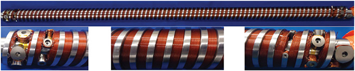
Figure 1. 1.2 m long NbTi helical undulator with 31.5 mm period and 31 mm magnetic bore developed for APS storage ring. Reproduced from [13]. CC BY 4.0.
Download figure:
Standard image High-resolution imageThe helical SCU is also of great interest in the application in the electron–positron collider. In 1991, Kezerashvili et al reported the fabrication of an 8-period NbTi helical SCU24 for measuring the polarization of the electron–positron colliding beams in the VEPP-2M storage ring; this short device reached an on-axis field B0 of 0.47 T at 18 mm vacuum bore (20 mm magnetic bore) but failed due to the signal-to-noise ratio in the spatial distribution of backscattered gamma-rays [15]. In 2002, Mikhailichenko and Moore winded a mini-helical SCU prototype with merely one layer NbTi winding and reported that an on-axis field B0 of 0.34 T could be reached at 2.42 mm period and 0.9 mm vacuum bore [16]. Since 2005, a series of NbTi helical SCU models had been constructed and tested for the demonstration of being used in the International Linear Collider (ILC) to produce polarized positrons with circularly polarized γ-ray sources in excess of 10 MeV. As reported by Ivanyushenkov et al [17–19], five short NbTi helical SCU models wound with NbTi ribbons were made to study the key parameters required for obtaining high on-axis field B0 under stable operation, i.e. No. of wires in one ribbon, No. of layers, winding bore, period length, mandrel material and impregnation technique. In 2008, Clarke et al reported the construction of a full scale SCU module for ILC and demonstrated that both two 1.74 m long helical SCU11.5 prototypes could reach a stable on-axis field B0 of 0.86 T at 5.23 mm vacuum bore (6.23 mm magnetic bore) after training quenches (Bm ∼ 1.13 T) [20]. In 2011, Scott et al experimentally demonstrated that a full-scale 4 m long working helical SCU module shown in figure 2 was suitable for future TeV-scale linear positron sources [14].

Figure 2. Four of the short NbTi helical prototypes and a 4 m long cryomodule containing two 1.74 m long undulators developed for ILC positron source. Reprinted figure with permission from [14], Copyright (2011) by the American Physical Society.
Download figure:
Standard image High-resolution image2.1.2. Nb3Sn helical.
A short Nb3Sn helical SCU14 model with return-peg design, as shown in figure 3, was first constructed by Kim et al in 2007 for the ILC positron source project; it is based on the wind-and-react technology and reached an on-axis field B0 of 0.9 T at 7.94 mm magnetic bore after training quenches [21]. With similar configuration, Majoros et al fabricated another two short models: one reached a low B0 of 0.314 T due to unexpected flux jumps and the other reached an enhanced B0 of 0.8 T by using small-filament Nb3Sn wires [22, 23].
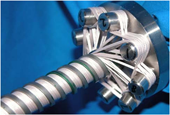
Figure 3. Nb3Sn helical undulator prototype with return-peg design. © 2007 IEEE. Reprinted, with permission, from [21].
Download figure:
Standard image High-resolution image2.1.3. MgB2 helical.
With a similar configuration as shown in figure 3, Majoros fabricated the first MgB2 helical SCU14 model in 2008 and demonstrated it could reach an on-axis field B0 of 0.25 T [24]. No further R&D works on MgB2 helical SCUs was later followed, possibly because of the low Jc in MgB2 wires at high magnetic fields.
2.1.4. Bulk HTS helical.
In 2018, a double staggered-array BHTSU shown in figure 4 was proposed by Calvi from Paul Scherrer Institute (PSI) for obtaining a helical on-axis field [25]. According to numerical studies, the double staggered-array bulk superconductors after field cooled (FC) magnetization from 10 T could generate an on-axis helical field B0 of 1.6 T at 10 mm period and 4 mm magnetic bore. This new helical undulator concept is of great interest to future compact FELs, but short prototype studies are required to demonstrate its feasibility.
Figure 4. Double staggered-array bulk HTS helical undulator. Reproduced with permission from [25].
Download figure:
Standard image High-resolution image2.2. Planar SCU
2.2.1. VR NbTi planar.
[Europe] The concept of vertical racetrack (VR) NbTi coils based SCU was first proposed by Bazin et al; the first device, consisting of vertically arranged NbTi racetrack coils and an inverse T-shape vacuum chamber, reached an on-axis field B0 of 0.4 T at 40 mm period and 12 mm vacuum gap (22 mm magnetic gap); this planar SCU40 device was later tested at ACO storage ring, showing reliable operation and emitting ultraviolet light at the beam energy of 140 and 240 MeV [29, 30]. In 1997, Hezel et al proposed the concept of a novel in-vacuum planar SCU consisting of vertically arranged NbTi solenoid coils; an 100-period device with 3.8 mm period (B0 = 0.56 T @ 1 mm magnetic gap) was later tested with an 855 MeV electron beam at the Mainz Microtron MAMI, showing reliable operation at beam current of up to 50 μA continuous-wave (CW) [31–33].
Since the 2000s, Karlsruhe Institute of Technology (KIT) has been working on the development of VR NbTi planar SCUs for the KIT synchrotron, previously known as Angströmquelle Karlsruhe (ANKA) storage ring. In 2002, a 10-period SCU14 model was first reported by Rossmanith et al obtaining an on-axis field B0 of 1.33 T at 5 mm magnetic gap [34, 35]. In 2006, an 100-period in-vacuum SCU14 device was developed under the collaboration between KIT and ACCEL Instruments GmbH and obtained an on-axis B0 of 0.38 T in the middle and decayed field amplitude at both ends at 7.4 mm vacuum gap (8 mm vacuum gap); this device was later tested with electron beam in the KIT synchrotron, showing reliable operation against the resistive wall wakefields effect and obtaining expected x-ray spectrum [36]. Afterwards, KIT and Noell GmbH started a collaboration to develop SCUs for the KIT synchrotron and low emittance light sources. Within this collaboration a SCU with period 15 mm and a magnetic length of 1.5 m was developed in 2011, obtaining an on-axis B0 of 0.73 T at 8 mm magnetic gap and a RMS phase error of 7.4° over a length of 0.795 m; this SCU device was later integrated into a conduction cooled cryostat with 7 mm vacuum gap as shown in figure 5(a) and commissioned in the KIT synchrotron with reliable operation at 2.5 GeV thanks to good thermal decoupling between the coil assembly and the 10 K liner [26, 37, 38]. During this time period, one short mock-up coil was fabricated for the demonstration of period length switching between 15 mm and 45 mm [39] and two different short mock-up coils were fabricated precisely for the demonstration of small pole height deviation [40]. In 2016, a 30 cm long SCU20 model shown in figure 5(b) was tested at CASPERII with obtained on-axis field B0 of 1.2 T at 8 mm magnetic gap [28]. In 2017, a 1.5 m long SCU20 device was developed in a collaboration between KIT and Noell GmbH with obtained on-axis B0 of 1.18 T at 7 mm vacuum gap (8 mm magnetic gap) and it was later commissioned in KIT synchrotron with its emitted 7th harmonic at the NANO beamline agreeing well with magnetic measurement results, showing superior performance than other undulator technologies [41, 42]. It should be mentioned that no quenches have been observed during user operation for both SCU15 and SCU20 devices. The collaboration between KIT and Noell GmbH lead to a successful commercialization of SCUs: a superconducting wiggler (SCW) device based on the same technology for the National Synchrotron Light Source II storage ring and a SCU device for the Australian Nuclear Science and Technology Organization (ANSTO) storage ring are being built. In 2019, Casalbuoni et al presented the design of a 0.41 m long SCU with switchable period length of either 17 or 34 mm by changing the current directions and experimentally validated this concept with short models (1.3 T @ 17 mm period, 2.3 T @ 34 mm period) [43].

Figure 5. (a) NbTi planar SCU15 installed in the KIT synchrotron. (b) 30 cm long NbTi planar SCU20 mock-up coil developed by the collaboration between KIT and Noell GmbH. © 2016 IEEE. Reprinted, with permission, from [28]. (c) NbTi planar SCU18-1 installed in the APS storage ring. (a), (c) Reproduced from [26]. CC BY 3.0. Reproduced from [27]. CC BY 4.0.
Download figure:
Standard image High-resolution imageR&D efforts on short-period VR NbTi SCUs were also ongoing in UK since 2010 [44, 45]; several 300 mm long SCU15 models were made to assess the design and manufacturing processes [46, 47]; even though not reaching the designed operation current Iop, an in-vacuum mini-undulator consisting of four 300 mm SCU modules was finally commissioned in a 50 MeV Compact Linear Accelerator for Research and Applications, demonstrating the reliable operation of in-vacuum SCU with electron beams [48].
SCUs also benefit European XFEL (EuXFEL). The use of SCUs would enable lasing at very high photon energy towards 100 keV, enhance the tuning range of photon energies up to a factor of 10 for soft x-ray SASE beamlines and allow the SASE line to cover the same photon energy range at a reduced LINAC energy of 7–8 GeV in CW operation mode [49, 50]. In 2021, Casalbuoni et al proposed to develop a SCU afterburner at the SASE2 hard x-ray beamline of EuXFEL for producing an output of 1010 ph/pulse at photon energies above 30 keV. The afterburner consists of five undulator modules with each one having two 2 m long VR SCU coils and one phase shifter. A pre-series prototype module (S-PRESSO) with a period of 18 mm, B0 of 1.82 T and vacuum gap of 5 mm will be built first to test the alignment, mechanical tolerances and implementation in the accelerator downstream the present SASE2 PM undulator line. Tests with electron beam are foreseen.
[U.S.A] In 1990s, Brookhaven National Laboratory (BNL) initiated the R&D on VR NbTi planar SCUs with 8.8 mm period and 4.4 mm magnetic gap for a 500 nm FEL experiment: the first 3-period model was continuously wound with a NbTi wire, obtaining an on-axis field B0 of 0.5 T; further experiments on three 23-period prototypes reached similar magnetic performance and a low phase error between 1.2° and 3.4°; unfortunately, these prototypes were not finally commissioned in the FEL experiment [51, 52].
Since 2000s, Argonne National Laboratory (ANL) has been working on the development of VR NbTi planar SCUs for APS storage ring. In 2004, two short mock-up coils were first reported by Kim et al with measured minimum quench energy at varying operating current up to 0.998Ic [53]. In 2013, a 330 mm long SCU16 device was reported by Ivanyushenkov et al with obtained on-axis field B0 of 0.8 T at 7.2 mm vacuum gap (9.5 mm magnetic gap) and it was later commissioned in Sector 6 of APS storage ring successfully for years, showing reliable operation and enhanced photon flux at energies above 50 keV [54, 55]. In 2015, the first 1.1 m long SCU18 device was reported by Ivanyushenkov et al with obtained on-axis field B0 of 0.98 T at 7.2 mm vacuum gap (9.5 mm magnetic gap) and it was later commissioned in Sector 1 of APS storage ring as shown in figure 5(c), showing outperformed photon flux in the high energy part of the x-ray spectrum and ∼100% availability [27, 56]. In 2016, the second 1.1 m long SCU18 device was developed with RMS phase error of 2° and replaced the old 330 mm long SCU16 in the APS storage ring [57]. At the moment of paper writing, there are several 1.9 m long, 16.5 mm period SCUs under construction at APS for the future upgraded storage ring [58].
As part of the Linac Coherent Light Source II (LCLS-II) SCU R&D collaboration, in 2018, ANL developed a 1.5 m long NbTi planar SCU21 model, obtaining an on-axis field B0 of 1.67 T at 8 mm magnetic gap and a RMS phase error of 5°, meeting all the basic requirements from LCLS-II [57]. Very recently, Stanford Linear Accelerator Center and ANL have proposed to test SCU performance at LCLS [49]; the SCUs (two or three undulator coils, 1.5 m long) will be installed as an afterburner at the hard x-ray beamline for testing the alignment and measuring the FEL gain.
[Asia] Since 2005, National Synchrotron Radiation Research Center (NSRRC) had been working on the development of VR NbTi planar SCUs for Taiwan Photon Source storage ring. In 2006, a 3-pole SCU15 upper-half coil was reported by Hwang et al with obtained operation current of 250 A, above the designed value [59]. In 2008, a 40-pole SCU15 model was reported by Jan et al obtaining an on-axis field B0 of 1.45 T at 5.6 mm magnetic gap and a small variation of 1.5% and 1.1% for the positive and negative fields, respectively [60]. In 2010, a 130-pole SCU15 model was developed with obtained on-axis field B0 of 1.36 T at 5.6 mm magnetic gap, after using an auto-shimming program based on adjusting the heights of iron pieces the phase error was reduced by ∼50% [61]. R&D efforts on VR NbTi planar SCUs were also made at Shanghai Institute of Applied Physics (SINAP) for the installation in Shanghai Synchrotron Radiation Facility (SSRF) storage ring. A 5-period SCU16 model was first reported by Xu et al with obtained on-axis field B0 of 0.93 T at 8 mm magnetic gap [62]. Most recently, a 50-period SCU16 device was successfully developed and tested at 200 mA beam current in the SSRF storage ring, obtaining a stable on-axis field B0 of 0.62 T at 7.5 mm vacuum gap (10 mm magnetic gap) [63, 64]. In 2019, the Institute of High Energy Physics (IHEP), Beijing initiated the R&D of SCUs for the high energy photon source under construction [65]. Very recently, a 0.5 m long SCU15 model was successfully developed and tested, obtaining an on-axis field B0 of 1.01 T at 7 mm magnetic gap and a RMS phase error between 4° and 10° at the operation current from 100 to 400 A [66].
2.2.2. VR Nb3Sn planar.
R&D efforts on VR Nb3Sn planar SCUs started at Lawrence Berkeley National Laboratory (LBNL) in 2003. The first six-period SCU30 half-coil was wound with a 6-strand Nb3Sn Rutherford cable, obtaining a quench current between 1700 and 2227 A (65%–80% short sample limit, SSL) in the first round test and above 2500 A after disconnecting the undulator half containing the suspect slice in the second round test [67, 68]. A second SCU14.5 half-coil was later developed for characterizing the field perturbation of the trim coil and studying the quench behaviour as it reached a quench current of 2633 A [69]. The third SCU14.5 half-coil was wound with a single Nb3Sn strand instead of a 6-strand cable, obtaining a quench current of 714 A (100% S.S.L.) [70]. In 2018, Arbelaez et al reported the test results of a new 1.5 m long SCU19 model developed for LCLS-II [5], showing an on-axis field B0 of 1.83 T (700 A, ∼80% SSL) could be obtained at 8 mm magnetic gap and the RMS phase error measured at 100 A could be reduced from 9.2° to 5.4° after local field tuning with YBCO current loops [48, 71].
Since 2005, ANL has also made great R&D efforts on VR Nb3Sn planar SCUs. Two short SCU14.5 coils were first fabricated, reaching a charging current density of 1.45 kA mm−2 and 1.92 kA mm−2 (90% SSL), respectively [75, 76]. For developing the technology required for a 3 m long SCU18 for the installation in APS storage ring, three 2.5-period Nb3Sn coils (MM1-3) were fabricated and tested in 2018 with the first one reaching only 70% SSL due to low field conductor instability and the second/third one reaching 96% S.S.L. with the use of fine filament Nb3Sn wires and the elimination of epoxy cracks [77], another four 4.5-period Nb3Sn coils (SMM3-6) were later fabricated and tested in 2019 with all reached >93% S.S.L [78]. In 2020, the first 0.5 m long Nb3Sn planar SCU18 model was developed in a collaboration between ANL and Fermi National Accelerator Laboratory (FNAL) but exhibiting insulation breakdown after an artificial quench at 700 A; the second 0.5 m long model shown in figure 6 was later developed with improved ground insulation and obtained an on-axis field B0 of 1.2 T @ 850 A at 9.5 mm magnetic gap [72]; the third 0.5 m long model was fabricated by removing the mica insulation for simplifying the winding process and delivered the required performance [79]. A 1.1 m long Nb3Sn planar SCU18 device is now under development in the collaboration between ANL and FNAL and planned to be installed in APS storage ring in 2022.

Figure 6. Second 0.5 m long Nb3Sn planar SCU prototype assembled at APS. © 2021 IEEE. Reprinted from [79], with necessary permissions from a contractor of the U.S. Government under Contract No. DE-AC02-06CH11357. Courtesy of ANL managed and operated by UChicago Argonne, LLC.
Download figure:
Standard image High-resolution image2.2.3. VR ReBCO planar.
In 2010, Boffo reported the design and test of the first VR ReBCO SCU coil assembly which employed a simultaneously winding scheme of bare superconductor and polyimide insulation, as shown in figure 7; the SCU coil, tested at KIT, reached a Je of 700 kA mm−2 at 4.4 K, thus equivalent to an undulator field as expected from a NbTi SCU coil [73]. In 2013, Nguyen et al reported the fabrication and test of a 3-period YBCO planar SCU14 model with 6 pancake coils on each half magnet array; the short model was measured in subcooled LN2 at 65 K and obtained an on-axis field B0 of 0.77 T at 3.2 mm magnetic gap [80]. In 2015, Kesgin et al reported the fabrication of a short no-insulation (NI) ReBCO SCU coil and experimentally studied the magnetic field decay induced by turn-to-turn current sharing effects [81]; by using a new U-slit tape configuration to reduce the number of resistive joints and an in-situ soldering technique during coil winding, a new short NI ReBCO SCU coil was fabricated and reached an operation Je of 1360 A mm−2 at 4.2 K [82]. In 2016, a novel continuously winding scheme was developed at ANL for fabricating two joint-free, 11-pole ReBCO SCU prototypes with NI and partial-insulation (PI) techniques, as shown in figure 8; it was demonstrated that the PI ReBCO coil could reach better performance with an operation Je of 2.1 kA mm−2 at 4.2 K [74]. In 2017, Kesgin et al developed a vacuum pressure impregnation technique, which was faster than the wet-winding but would not degrade the ReBCO coil performance by adding a bumper layer between the winding stacks and the epoxy/powder mixture [83]. R&D on short ReBCO planar SCU coils was also carried out at SINAP in 2018: a short SCU13 coil showed an early quench at 77 K and even worse performance after thermal cycles [84].
Figure 7. The first VR ReBCO SCU coil assembly employing a simultaneously winding scheme of bare superconductor and polyimide insulation. Reproduced with permission from [73].
Download figure:
Standard image High-resolution image
Figure 8. Continuously wound joint-free, 11-pole VR ReBCO planar SCU prototypes. Reproduced from [74]. © IOP Publishing Ltd. All rights reserved.
Download figure:
Standard image High-resolution image2.2.4. HR NbTi planar.
Budker Institute of Nuclear Physics (BINP) has more than 40 years of experience in developing horizontal racetrack (HR) NbTi coils based superconducting insertion devices for world-wide synchrotron light sources, i.e. superconducting wave length shifter with peak field from 7 to 10 T, high-field superconducting multi-pole wiggler (SCMPW) with period length between 140 and 200 mm and with peak field up to 7.5 T, middle-field SCMPW with period length between 46 and 64 mm and with peak field from 2.5 to 4.2 T, and low-field SCMPW with period length between 30 and 34 mm and with peak field from 2 to 2.5 T [85]. In 2016, Mezentsev et al for the first time reported the development of a 15-period HR NbTi planar SCU15.6 model with active/neutral poles and experimentally demonstrated that the prototype could reach an on-axis field B0 of 1.2 T at 8 m magnetic gap [86]. In 2017, Bragin et al reported the development of a 40-period SCU15.6 prototype and experimentally demonstrated that an on-axis field B0 of 1.2 T could be obtained after training quenches and the RMS phase error was ∼3.5°–4° [87]. In 2021, BINP reported the latest test of a 119-period SCU15.6 model, as shown in figure 9; this 2 m long model also reached an on-axis field B0 of 1.2 T after one thermal cycle and training quenches [88].
Figure 9. 2 m long HR NbTi planar SCU prototype developed at BINP. Reproduced with permission from [88].
Download figure:
Standard image High-resolution imageThe HR NbTi planar SCU combined with the in-vacuum concept has been selected as the option for the third hard x-ray beamline with photon energies between 10 and 25 keV for Shanghai HIgh repetitioN rate XFEL and Extreme light facility (SHINE) [88]. The whole beamline consists of forty 4 m long SCU modules which will be cooled by a large cryogenic plant; each SCU module is designed for obtaining an on-axis field B0 of 1.58 T at 16 mm period and 4 mm beam gap. Most recently, a 4 m long SCU prototype is developed and waiting to be tested using the LHe cryo-plant.
2.2.5. Meander-type ReBCO planar.
In 2009, Prestemon et al proposed a new concept of short-period meander-type ReBCO planar SCU in which the transport current flowed in the predefined path in the tape stacks, generating an on-axis sinusoidal field as shown in figure 10(a) [89]; the feasibility of adopting this new undulator concept in future FEL applications was later studied with an emphasis on the impact of the machining tolerances on the field errors [91]. In 2013, Holubek et al experimentally demonstrated >10 mT on-axis sinusoidal field at 2 mm above the center of a single meander-type YBCO tape structured with picosecond laser pulses [92]. In 2017, Holubek et al proposed a novel winding scheme named JUST for making a jointless meander-type ReBCO planar SCU, as shown in figure 10(b); the numerical simulation indicated that an on-axis field B0 of 0.5 T could be obtained at 4 mm magnetic gap in a meander-type SCU8 consisting of thirty 12 mm wide, copper-free ReBCO tape stacks in each coil module [90].

Figure 10. (a) Basic concept of a meander-type ReBCO planar SCU. Reproduced from [89]. CC BY 3.0. (b) Winding scheme of a joint-free meander-type ReBCO planar SCU. Reproduced from [90]. © IOP Publishing Ltd. All rights reserved.
Download figure:
Standard image High-resolution image2.2.6. Hybrid PM-HTS planar.
In 2004, Tanaka et al proposed a new scheme for enhancing the on-axis undulator field by combining the PM undulator with bulk HTS rings, as shown in figure 11; the idea was to FC magnetize the HTS rings during opening the magnetic gap to compensate the field loss; experimental results validated this novel concept and it was pointed that good mechanical stability and high Jc in bulk HTS rings were necessary [93]. R&D towards improving the mechanical properties of the bulk HTS ring by resign impregnation and iron ribbing were later carried out [94, 95], however, no more undulator models based on this technology were later developed.

Download figure:
Standard image High-resolution image2.2.7. Pure-type bulk HTS planar.
In 2005, Tanaka et al proposed the concept of pure-type BHTSU which utilized a dipole coil to FC magnetize a series of rectangular HTS bulks as shown in figure 12; this new concept was experimentally validated at 59 K with applied field of up to 2 T, but showing a number of technical challenges [96]. A series of modelling works on this SCU concept were later carried out by Yi et al based on the finite difference method (FDM) and on either the critical state model or the E-J power law model [97–99], but no more undulator models based on this technology were later developed.
Download figure:
Standard image High-resolution image2.2.8. Staggered-array bulk HTS planar.
R&D on staggered-array BHTSU started at Kyoto University in 2006. Kii et al first proposed the concept of staggered-array BHTSU which utilized a solenoid field to magnetize staggered-array half-moon shaped YBCO bulks as shown in figure 13(a) and experimentally demonstrated that an on-axis sinusoidal field could be obtained at 77 K [100]. In 2008, Kinjo et al successfully tuned the amplitude of on-axis field in a 3-period model by reversing the applied solenoid field and validated the experimental results with numerical simulations [101]. Later, Kii et al measured the bulk superconductor's magnetic performance at the temperature range from 4 to 77 K and numerically studied the impact of Jc variation in ReBCO bulks on the field error based on the critical state model and loop current assumption [102, 103]. In 2013, Kinjo et al first experimentally demonstrated that a 6-period BHTSU10 model shown in figure 13(b) could obtain an on-axis field B0 of 0.85 T @ 6 K at 4 mm magnetic gap by employing a 2 T solenoid to execute FC magnetization from −2 T to 2 T and then numerically studied the BHTSU model by using an analytical approach and the magnetic energy minimization method [104, 105]. In 2017, Kii et al proposed the conceptual design of a staggered-array bulk MgB2 undulator and indicated that the robust MgB2 bulk could reduce the peak field variation to lower than 1% [106], but real models have not been reported yet.
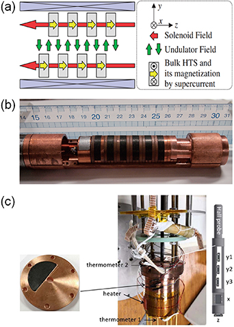
Figure 13. (a) Concept of a staggered-array bulk HTS undulator; (b) 4 mm gap and 10 mm period staggered-array BHTSU prototype fabricated at Kyoto University. Reproduced from [104]. © IOP Publishing Ltd. All rights reserved. (c) 6 mm gap and 10 mm period staggered-array BHTSU prototype fabricated at Cambridge University. Reproduced from [107]. © IOP Publishing Ltd. CC BY 3.0.
Download figure:
Standard image High-resolution imageIn 2013, NSRRC reported the experiment on a 5-period staggered-array BHTSU model with 5 mm period and 4 mm magnetic gap, but the measurement on-axis field profile was quite far from expectation possibly due to the saturation or Jc inhomogeneity in ReBCO bulks [108]. Further experiments on mapping the field profile above different field-trapped ReBCO bulks showed inconsistent results and the necessity to improve the bulk's quality [109].
Since 2018, PSI, in collaboration with Cambridge University, has been working on the R&D of short-period staggered-array BHTSU for SwissFEL and Swiss Light Source 2.0 (SLS2.0) storage ring [3, 25]. In 2019, Calvi et al experimentally demonstrated that a 5-period BHTSU10 model shown in figure 13(c) could obtain an on-axis field B0 of 0.85 T at 6 mm magnetic gap after FC magnetization with ΔBs = 7 T at 10 K and that further increase of ΔBs would result in a premature quench [107]. Numerical simulations were later carried out by Hellmann et al with COMSOL H -formulation for understanding the complex correlation between B0 and design parameters and by Zhang et al with ANSYS A -V formulation based backward computation method for optimizing the on-axis field integrals in a 10-period staggered-array 3D BHTSU model [110–112]. In 2021, it was experimentally demonstrated that a 10-period BHTSU10 model could obtain an on-axis field B0 of ∼1.54 T @ 10 K at 4 mm magnetic gap and that a subcooling from 10 K to 8 K could help to freeze the trapped magnetic flux in GdBCO bulks, resulting in a long decay time constant of 3.2 years [3].
A 1 m long staggered-array BHTSU device, aiming at allowing experiments to be carried out at photon energies above 60 keV, has been scheduled for the I-TOMCAT beamline at SLS2.0 under the collaboration between PSI and FNAL. More details of the design can be found in section 4.1.
2.3. Variably polarized SCU
2.3.1. Hybrid planar-tilted type.
The concept of generating elliptical on-axis field with tilted superconducting racetrack coils was first proposed by Walker [113]. In 2004, Hwang et al pointed that the circular polarization provided by tilted SCU coils was more efficient than that from a staggered undulator [114, 115]; by integrating two planar magnet arrays into the tilted structure as shown in figure 14, it was possible to obtain six polarization modes by switching the operation currents, i.e. right elliptical polarization, left elliptical polarization, right circular polarization (RCP), left circular polarization (LCP), vertical polarization (VP) and horizontal polarization (HP) [116]. Similar studies on this hybrid planar-tilted type SCU were later presented in [117–119]. In 2009, Chen et al fabricated a short hybrid planar-tilted SCU24 model and demonstrated that an on-axis helical field of 0.61 T could be obtained for both Bx and By with proper operation currents (Iin = 380 A, Io = 449 A) [120]. In 2020, Kanonik et al fabricated a 15-period SCU22 model and demonstrated that an on-axis field of 1 T vertically and 0.7 T horizontally (elliptic coefficient of 0.7) could be obtained at 8 mm magnetic gap [121].
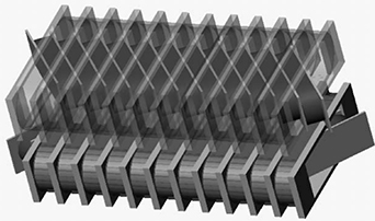
Figure 14. Concept of hybrid planar-tilted SCU with variable polarization. Reproduced from [116]. CC BY 3.0.
Download figure:
Standard image High-resolution image2.3.2. Double-helical type.
The concept of double-helical electromagnetic undulator was first proposed by Alferov D F in 1976 and later numerically studied by Ivanyushenkov et al for a universal SCU as shown in figure 15 [122, 123]; by switching the operation currents in two helical coils, four polarization modes could be realized, i.e. RCP, LCP, VP and HP.
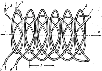
Figure 15. Concept of universal double-helical SCU with variable polarization. Reproduced from [123]. CC BY 3.0.
Download figure:
Standard image High-resolution image2.3.3. Apple/Delta type.
In 2005, Prestemon et al proposed an APPLE-like SCU in which variable polarization modes could be obtained by switching the operation currents, as shown in figure 16(a); with period doubling, this new concept SCU could yield significantly enhanced spectral range [124]. In 2017, Ivanyushenkov et al proposed another Delta-like superconducting arbitrarily polarizing emitter (SCAPE) undulator which was capable of generating either planar or circularly polarized photons by switching the operation currents as shown in figure 16(b); the on-axis field in SCAPE could be maximized with a small-diameter round beam chamber, which was achievable in DLSRs and FELs [125]. In 2019, Kasa et al reported the experiments on a first 0.5 m long SCAPE model and demonstrated that an on-axis field greater than 0.6 T for both Bx and By could be obtained at 30 mm period and 6 mm vacuum bore [126].

Figure 16. (a) Apple-like SCU proposed by Prestemon et al. © 2006 IEEE. Reprinted, with permission, from [124]. (b) concept of SCAPE undulator with recessed triangular coils and magnetic poles. Reproduced from [125]. CC BY 3.0.
Download figure:
Standard image High-resolution image2.3.4. Double-planar type.
In 2020, Kanonik et al proposed the concept of 40 mm period superconducting undulators with variable polarization (SCUVP) which consisted of two identical planar undulator arrays placed mutually perpendicular, as shown in figure 17; by switching the operation currents, planar or elliptical on-axis field with different elliptic coefficients could be realized easily [127].
Figure 17. Concept of a double-planar type SCUVP undulator. Reprinted from [127], with the permission of AIP Publishing.
Download figure:
Standard image High-resolution image3. SCU design and theory limits
3.1. Overview of type-II superconductors
Short period SCUs are of great interest to both synchrotrons and FELs in either enhancing the photon energy or reducing the overall facility cost. But for reaching the very hard x-ray regime, a tunable K value up to 2 is appreciated in general, namely we have to ensure the effective undulator field is large enough at short periods, e.g., 1.43 T at 15 mm period and 2.14 T at 10 mm period. In such a case, high-performance superconductors are highly desired by SCUs.
Figure 18 summarizes the whole conductor critical current density Je in state-of-the-art commercial low- and high-Tc type-II superconductors under applied magnetic fields up to 12 T. Data points are extracted from NbTi LHC wire [128], RRP Nb3Sn wire [129], AIMI MgB2 wire [130], Sumitomo Bi-2223 tape [131], 50 bar OPHT Bi-2212 wire [132], Superpower ReBCO tape [133], QMG-GdBCO bulk [105], and ATZ-YBCO bulk [134]. The Je data above 12 T are omitted because SCUs are usually designed with low coil field but large current density and associated on-axis field B0. It can be found that the low-Tc MgB2 and Nb-Ti wires and the high-Tc Bi-2223 tape show obviously lower Je than the others at 4.2 K. Other useful information is summarized as follows: (a) the ReBCO coated conductor shows much higher Je at B//tape than at B⊥tape; (b) the 50 bar OPHT Bi-2212 round wire has good isotropic material property and its Je level at 4.2 K lies in between the ReBCO tape's performances at B//tape and B⊥tape; (c) the RRP Nb3Sn wire shows higher Je than ReBCO tape at B//tape when the applied field is below 5 T, having great potentials for being applied in SCUs; (d) both QMG-GdBCO and ATZ-YBCO bulk superconductors show significantly larger Je than the others at 4.2 K due to the lack of copper/silver matrix or Hastelloy substrates, importantly, the GdBCO bulk at 10 K shows higher Je than Nb3Sn wire at 4.2 K.
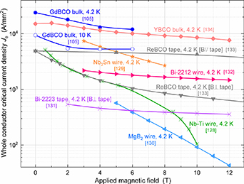
Figure 18. Whole conductor critical current density Je in commercial low- and high-Tc superconductors under applied magnetic fields up to 12 T.
Download figure:
Standard image High-resolution imageApart from commercially available type-II superconductors, R&D efforts towards improving high-Tc superconductors were continuously made to meet the demands of high-field magnet applications. Very recently, Majkic et al from the University of Houston experimentally demonstrated that by increasing the thickness of HTS layer up to >4 μm with an advanced MOCVD system a whole ReBCO conductor critical current density Je greater than 5 kA mm−2 could be obtained at 14 T [135]. It should be mentioned that such high Je was tested at applied field parallel to the c-axis of the tape (B⊥tape) and it could be even higher at B//tape. Recent advances in long-length (>100 m) Sr0.6K0.4Fe2As2 iron-based superconductor (IBS) tape bring interests for its application in accelerator magnets [136]. As shown in [137], state-of-the-art IBS tape processed with hot-pressing obtained a Je of 300 A mm−2 at 4.2 K and 10 T, but there is still large room for being advanced [138]. In 2014, Durrell et al trapped a record field 17.6 T at 26 K in silver doped, melt-processed GdBCO bulks [139]. The GdBCO bulk is silver doped for enhancing its mechanical performance and pre-stressed by a shrink-fitted stainless steel for avoiding a premature quench. The high-performance GdBCO bulks were later utilized for developing a 5-period undulator prototype and tested at the University of Cambridge [107]. Most recently, a new record-high trapped field of 5.6 T at 11 K was obtained in MgB2/TiB2 composite bulks processed by hot isostatic pressing [140], however, MgB2 bulks were still far from being utilized for application in short period undulators due to their low Je.
3.2. Overview of SCU design
3.2.1. Design requirements.
SCUs, with effective K value often below 3, have smaller period length and lower on-axis field in comparison to SCWs. For magnetic design, it is essential to ensure a safety margin of ∼20% by optimizing the superconductor size, the period length λ, the magnetic gap g and the coil dimensions so that the operation current Iop and the associated peak coil field Bm is far from the S.S.L. given in figure 18. With regards to superconducting racetrack coils based planar undulator, there is no clear answer yet whether the VR scheme is superior to the HR one. The VR planar SCU can go to much shorter periods due to the large coil winding radius and less splices required, but it is less efficient requiring much longer superconductors and more difficult to be pre-stressed with external compression.
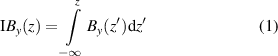
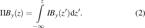
Aimed at providing coherent light in a storage ring or FEL, the SCU module has to reach good manufacturing accuracy and low RMS phase error. When electron bunches travel along an undulator they are expected to oscillate in the plane or move forward spirally, emitting coherent light sources. After experiencing the undulator field the electron bunches must follow their original moving directions without an off-axis offset or an angle shift, namely the first and the second integral of the on-axis By shown in equations (1) and (2) need to be minimized by optimizing the coil ends and adding correction coils
There are few concerns on the mechanical design or stress management in SCUs possibly because the magnetic energy and the associated magnetic forces are much lower than in high field superconducting accelerator magnets or wigglers. However, if applicable it is still necessary to pre-stress well the SCU coil assembly to prevent a premature quench due to flux jumps, for example, in the staggered-array BHTSU [107].
For quench protection, a general requirement of the hot spot temperature in superconducting coils is no higher than 350 K to avoid breaking the insulations due to large temperature or thermal stresses. This can be done either with a passive quench protection system incorporating parallel diodes in which most of the supply current will go through the diodes and the coil current decays rapidly after quench propagates [67] or with an active quench protection system incorporating an external dump resistor in which the magnetic energy is extracted externally after detecting a quench [72]. Based on the adiabatic model, one can evaluate the peak hot spot temperature Tm in SCU coil windings efficiently according to the MITTs value shown in equation (3)
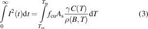
where I(t) is current at time t, Tcs is current sharing temperature, fcu is copper/superconductor ratio, As is superconductor area, C(T) is temperature-dependent specific heat capacity, ρ(B,T) is copper resistivity at certain magnetic field and temperature.
3.2.2. Modelling tools.
In 1990, Ben-Zvi first adopted the FDM software POISSON for the 2D magnetic analysis of a VR NbTi planar SCU for FEL application [51]. In 1998, Hezel et al first reported using the finite integral method software MAFIA for the field calculation of a vertical NbTi pancake coils based SCU for MAMI experiments [32]. In 2000, Rossmanith et al first adopted the boundary integral method-based RADIA code (implemented in Mathematica) for the magnetic field calculation of an in-vacuum planar SCU [141]. Further studies based on RADIA code were reported for the magnetic design or field optimization of planar SCU [59, 142–144], hybrid planar-tilted SCU [117, 120], staggered-array BHTSU [108], Delta-like SCAPE undulator [125] and NbTi helical SCU [13]. In 2002, Caspi et al first adopted the finite element method (FEM) software TOSCA/OPERA 2D for the magnetic design of helical windings based planar SCU [145]. Further studies based on OPERA 2D/3D code were reported for the magnetic design or field optimization of planar SCU [44, 67, 146–148], helical SCU [17, 149, 150] and double-helical SCU [123]. In 2005, Alexeev et al first adopted the FEM software ANSYS for calculating the magnetic field in a helical SCU designed for a MIR-FEL experiment [11]. Further studies based on ANSYS were reported for the magnetic and mechanical design study of Nb3Sn planar SCU [77, 151] and staggered-array bulk HTSU [111, 112, 152]. In 2010, Majoros et al first adopted the FEM software FLUX 3D for simulating the magnetic fields in a 3D Nb3Sn helical SCU model [22]. In 2013, Zhong et al adopted the FEM software COMSOL for simulating the magnetic fields in a staggered-array bulk HTSU with the H -formulation method [153]. Further work on modelling HTS undulators with COMSOL were reported by Nguyen and Ashworth [80] and Hellmann et al [110]. In 2019, Casalbuoni et al reported the magnetic design of a planar SCU with period length doubling based on the FEM software FEMM [43]. Other numerical methods, like the magnetic energy minimization method and the T -method based FDM, were widely used for the magnetic analysis of pure-type, staggered-array and hybrid PM-HTS bulk SCUs [97, 105, 108, 154].
3.2.3. Scaling laws.
Commercial FEM software or other modelling tools are essential in designing a SCU due to the special relation between the critical current Ic and peak coil field Bm. But it is also of interest to quickly evaluate the on-axis undulator field B0 in SCUs using analytical formulations when the operation current Iop and key geometric parameters are given, neglecting whether Iop is feasible or not.
Referring to the helical solenoid field equation proposed by Smythe [155], Kim proposed the first analytical formulation equation (4) in 2006 for calculating the on-axis field B0 in a helical SCU shown in figure 19 [156]
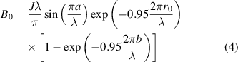
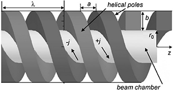
Figure 19. Calculation model helical SCU. Reprinted from [156], Copyright (2007), with permission from Elsevier.
Download figure:
Standard image High-resolution imagewhere J, λ, r0, a and b refer to current density, period length, bore diameter and the coil dimensions in z- and r-directions, respectively. In 2002, Moser et al proposed a simple analytical formulation for calculating the on-axis field B0 in a planar SCU, as shown in equation (5)
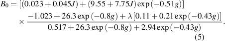
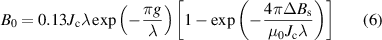
Other scaling laws were later proposed by Kim for a planar SCU with fixed Jλ [157] and by Mishra for a 14 mm period planar SCU based on the formula for a hybrid PM undulator [144]. In 2014, Kinjo et al presented an analytical formula equation (6) for calculating the on-axis field B0 in a staggered-array bulk HTSU and validated it through experiments
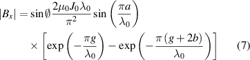
where  is magnetic field change, μ0 is vacuum permeability, Jc is critical current density [105]. In 2005, Kim et al presented an analytical formula for calculating the on-axis horizontal field Bx
in a planar-tilted hybrid SCU [118], as shown in equation (7)
is magnetic field change, μ0 is vacuum permeability, Jc is critical current density [105]. In 2005, Kim et al presented an analytical formula for calculating the on-axis horizontal field Bx
in a planar-tilted hybrid SCU [118], as shown in equation (7)
where  , as is shown in figure 20;
  is rotation angle, J0 is current density, a is coil width, b is coil height.
Figure 20. Top view of the rotated coils of the inserted unit. © 2005 IEEE. Reprinted, with permission, from [118].
Download figure:
Standard image High-resolution imageMore field scaling laws summarized recently for different types of SCUs can be found in the CompactLight design report [158].
3.3. SCU optimization and theory limits
3.3.1. Periodical FEA models and design optimization.
The above numerical simulations and scaling laws were essential in understanding the performances of different types of SCUs, however, a systematic comparison study in SCUs and CPMUs is missing. In this section, we try to fill in this gap by creating undulator models in ANSYS parametrical design language, implementing state-of-the-art Je for low- and high-Tc superconductors and remanent field Br for cryogenic PMs and conducting the design optimization using the ANSYS zero-order optimization module. Figure 21 presents the 2D/3D periodical FEA models for SCUs and CPMUs. The reason for creating periodical models is that the computation time can be shortened significantly for executing an automatic design optimization. The periodical boundary can be applied by coupling the magnetic vector potential A for the matching nodes in the periodical boundary lines or areas.

Figure 21. Periodical FEA models created in ANSYS. (a) 2D NbTi/Nb3Sn planar SCU model; (b) 2D VR ReBCO planar SCU model; (c) 2D HR ReBCO planar SCU model; (d) 2D staggered-array bulk ReBCO planar SCU model; (e) 3D NbTi/Nb3Sn helical SCU model; (f) 3D ReBCO helical SCU model; (g) 2D Halbach CPMU model; (h) 2D hybrid CPMU1 model; (i) 3D hybrid CPMU2 model.
Download figure:
Standard image High-resolution imageIn superconducting coils based SCUs (figures 21(a)–(c), (e) and (f)) with certain period length λ and magnetic gap/bore g/r1, the design variables (DVs) include the geometry sizes—coil width w, coil height h, outer radius r2 and the operation current density Jo; the state variables (SVs) include the peak coil field Bm and the loadline ratio LL (Jo/Je). ReBCO coil-based planar and helical undulator models are created with multi-layers to take into account the anisotropic material property of ReBCO tapes whose Je is a function of the magnetic field components:  , as shown in equation (8)
where Je0 refers to the engineering current density at zero field and 4.2 K; k, Bc, and b are fitting coefficients. After each optimization step, the critical current Ic in each ReBCO layer is updated with the sum of Je
Ae (Ae is element area) for all associated elements in this layer; the ReBCO layer with lowest Ic (or  ) is then selected as the design limit and the loadline ratio LL is updated with Jo/
 . In the staggered-array BHTSU model with certain λ and g, the DVs include the geometry sizes—coil width w, coil height h and the magnetization field change ΔBs; no SVs are required to constrain the analyses. The magnetization of staggered-array BHTSU is simulated by using a fast and efficient backward computation method implemented in ANSYS [111, 112]. In the Halbach type and two hybrid-holmium CPMUs with certain λ and g, the DVs include the geometry sizes—magnet width w, magnet height h, total length l2 and the holmium length l1; no SVs are required to constrain the analyses. In all undulator models, the target is searching for the minimum objective (OBJ) function equation (9), i.e. maximum B0, from feasible solutions

where B0 refers to the amplitude of the on-axis undulator field. The settings of DVs, SVs and OBJ in different types of SCUs and CPMUs are summarized in Table 2.
Table 2. Settings of design variables (DVs), state variables (SVs) and objective (OBJ) in different type SCUs and CPMUs for optimal design.
| DVs | SVs | OBJ | ||||||||
|---|---|---|---|---|---|---|---|---|---|---|
| w | h | r2 | Jo | ΔBs | l1 | l2 | Bm | LL | |10−B0| | |
| NbTi/Nb3Sn planar |

|

|

|

|

|

| ||||
| VR ReBCO planar |

|

|

|

|

|

| ||||
| HR ReBCO planar |

|

|

|

|

|

| ||||
| Bulk ReBCO planar |

|

|

|

| ||||||
| NbTi/Nb3Sn helical |

|

|

|

|

|

| ||||
| ReBCO helical |

|

|

|

|

|

| ||||
| Halbach CPMU |

|

|

| |||||||
| Hybrid CPMU1 |

|

|

| |||||||
| Hybrid CPMU2 |

|

|

|

|

| |||||
During optimization, ANSYS establishes a relation between the OBJ and DVs and a relation between SVs and DVs through calculating the OBJ and SVs from a series of sets of DVs and conducting the least squares fit between all the data points. The constraints on the SVs are converted to an unconstrained optimization problem by adding penalties to OBJ to take into account the imposed constrains. Then the ANSYS program searches the minimum value of the augmented objective function  by using a sequential unconstrained minimization technique (SUMT) at each iteration step. Assuming the peak coil field Bm is restricted to no greater than 12 T and the loadline ratio LL is restricted to lower than 1 in a superconducting coils based SCU, the augmented objective function
  can be expressed as
where  is the penalty factor and set to a very large value. When Bm or LL does not meet the constraints, OBJa
will have a very large value and the associated DVs are treated as infeasible solutions. The iteration process terminates when the optimization converges, namely the change in OBJa
between current value and the minimum or the change in OBJa
between last two solutions is lower than the setting tolerance
is the penalty factor and set to a very large value. When Bm or LL does not meet the constraints, OBJa
will have a very large value and the associated DVs are treated as infeasible solutions. The iteration process terminates when the optimization converges, namely the change in OBJa
between current value and the minimum or the change in OBJa
between last two solutions is lower than the setting tolerance  , as shown in equations (11) and (12)


3.3.2. Optimal on-axis undulator field.
During optimal design, a high remanent field Br of 1.65 T is given to the PMs and the ferromagnetic material holmium with high saturation field is adopted in the two hybrid CPMUs; a filling factor of 80% is set for the superconducting coils based undulators and no ferromagnetic materials are considered in SCUs, allowing a ∼15% safety margin for the optimal field.
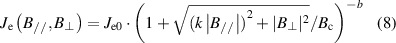
Figures 22 and 23 summarizes the optimal on-axis field B0 and K value in different types of undulators at varied period length λ and magnetic gap/bore g/r1. The conclusions are as follows
- (a)The theory limits of the undulator field for the Halbach CPMU and the hybrid CPMU1 are similar at varied λ and g.
- (b)The hybrid CPMU2 can generate slightly higher undulator field than the other two CPMUs at small magnetic gaps.
- (c)The NbTi planar undulator shows better performance than CPMUs when λ is larger than 12 mm. More detailed comparisons between NbTi SCUs and CPMUs are summarized in [159].
- (d)The HR ReBCO planar undulator shows much better performance than the VR ReBCO planar because the major magnetic flux lines are more parallel to the tape surface in the former case, enabling a larger critical current Ic in the weakest ReBCO tape.
- (e)Both Nb3Sn helical and HR ReBCO planar undulators show outstanding performances than the others at varied period lengths and magnetic bores/gaps.
- (f)The staggered-array bulk ReBCO planar undulator shows slightly weaker performance than the Nb3Sn helical and the HR ReBCO planar, but it works at 10 K and provides quite large safety margin for thermal management.
- (g)It is obvious that the helical SCU can generate higher on-axis field B0 than the planar one (Nb3Sn helical > Nb3Sn planar, ReBCO helical > VR ReBCO planar, NbTi helical > NbTi planar), not to mention the effective undulator field Beff in helical SCUs is
 times B0.
 - (h)For reaching a tunable K > 2 at period as short as 10 mm (dreamed for future compact light), the available solutions are Nb3Sn helical at 4.2 K and r1⩽ 6 mm, HR ReBCO planar at 4.2 K and g⩽ 4 mm, staggered-array bulk ReBCO planar at 10 K and g⩽ 4 mm, and ReBCO helical at 4.2 K and r1 ⩽ 5 mm.
- (i)It should be mentioned that the presented B0 refers to the magnetic limits while the mechanical feasibility, like winding bore/radius and thermal separation, is not taken into account in the optimal design. In addition, the direction of the c-axis in a ReBCO tape is not always necessarily perpendicular to the tape surface [160], meaning equation (8) can be modified and the corresponding B0 can be higher in a VR ReBCO planar undulator.


Figure 22. Relation between on-axis undulator field and magnetic gap/bore at period length: (a) 10 mm, (b) 12 mm, (c) 14 mm and (d) 16 mm.
Download figure:
Standard image High-resolution image
Figure 23. Relation between K-value and magnetic gap/bore at period length: (a) 10 mm, (b) 12 mm, (c) 14 mm and (d) 16 mm.
Download figure:
Standard image High-resolution image4. Technical challenges and outlook
4.1. SCU cryostat
State-of-the-art SCU prototypes served in synchrotron storage rings are all housed in a horizontal cryostat and cooled utilizing GM cryocoolers with or without liquid helium. The liner or vacuum chamber working at 10–20 K was utilized to absorb the heat load from the synchrotron radiation from upstream magnets, the resistive wall wakefields, and the electron and ion bombardment. In the KIT synchrotron, both SCU15 and SCU20 adopted a complete cryogen-free conduction cooled scheme: the superconducting coils, the thermal shield and the liner are cooled separately by four GM cryocoolers, as shown in figure 24(a) [40]. In APS storage ring, the commissioned SCUs including one SCU16, two SCU18 and one HSCU31.5 all adopted a thermosyphon scheme shown in figure 24(b): the superconducting coil assembly was indirectly cooled by liquid helium pipes; two GM cryocoolers were connected to the liquid helium tank to re-condense the helium gas; another two were utilized to cool the thermal shield and the liner, separately [56].

Figure 24. (a) Cryostat of SCU15 in ANKA storage ring. Reproduced from [26]. CC BY 3.0. (b) Cryostat of SCU0 in APS storage ring. Reproduced from [55]. CC BY 3.0. (c) Cryostat of staggered-array bulk HTS undulator for the planned I-TOMCAT beam line at SLS2.0.
Download figure:
Standard image High-resolution imageAnother design option of the cryostat is to immerse the SCU coil assembly into a liquid helium bath which is re-condensed by GM cryocoolers, but at the expense of losing mechanical gaps. The full-scale 4 m long NbTi helical SCU developed for ILC positron source was based on this design, but this SCU module was not tested with electron beam and remained to be validated in storage rings or FELs [14, 20].
All SCUs commissioned at the KIT synchrotron and APS storage ring have a cold vacuum chamber to thermally isolate the superconducting coil assembly from the electron beam. But it should be pointed that previously developed in-vacuum SCUs without a separate vacuum chamber also showed promising results [33, 34, 36]. For FEL experiments, in-vacuum SCU can be a good option because there is no synchrotron radiation from upstream bending magnets and the resistive wall wakefields induced heat load is low. As suggested by Clarke et al thin copper foils with high conductivity can be adopted to absorb the heat load and a single large cryo-plant can be employed to cool efficiently the long SCUs based x-ray FEL beamline [161]. An example is the recent design of in-vacuum SCUs for the SHINE hard x-ray beamline [162].
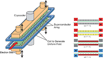
In figure 24(c) is a cryogen-free cryostat of a 1 m long staggered-array BHTSU module developed for I-TOMCAT beamline at SLS2.0 under the collaboration between PSI and FNAL. One GM cryocooler is utilized to conduction cool the superconducting solenoid and the thermal shield; another two are utilized to conduction cool the magnet bore to 20–35 K and the staggered-array ReBCO bulks to 10–100 K. The ReBCO bulks are kept at 100 K above Tc during ramping up the solenoid field and cooled to 10 K during ramping down slowly the solenoid field for magnetization.
4.2. Magnetic field measurement
When electron bunches travel along a SCU with low RMS phase error they are expected to oscillate, generating coherent light sources; after experiencing the on-axis undulator field, the electron bunches shall follow their original direction of motion without neither an offset nor an angle. This requires carefully tuning local magnetic fields and correcting the field integrals along the undulator axis based on advanced magnetic field measurement systems. In the following, we briefly summarize available magnetic field measurement techniques for SCUs, more details can be find in the review paper from Casalbuoni [163].
4.2.1. Hall probe scanning.
Hall probe scanning is so far the most mature technique for local field characterization of both PM and SCUs. Review of hall probes applied for measuring the room-temperature beam line magnets and PM undulators are made by Sanfilippo [164]. For accurate SCUs measurement, the temperature-insensitive InAs Hall sensor is a good option and the associated calibration at varied cryogenic temperatures and magnetic fields is necessary to understand the nonlinearity between Hall resistance, Vhall/Iop and magnetic field. In figure 25 is the calibration curve of a typical InAs Hall sensor at temperature from 2.2 to 18.3 K and field from 0 to 9 T. The InAs Hall sensor was calibrated with the physical property measurement system at PSI, showing good reproducibility. It can be concluded that quantum oscillation [165] occurs and grows with the rise of applied field and lower temperature can bring stronger quantum oscillation effect. Figure 26 shows possible measurement approaches with hall sensors. The first approach is using a cryogenic Hall sledge on guiding rails, as shown in figure 26(a); this approach has been widely used for measuring the on-axis field of SCUs at KIT [28]. The second approach is using an 'anticryostat' with room-temperature hall sensors fixed on a carbon fiber tube which is movable along a thermally isolated and tensioned titanium guiding tube [166], as shown in figure 26(b); this approach, without quantum oscillation effect in the Hall sensors, has been widely used for measuring the on-axis field of SCUs at ANL and SCWs at BINP. It should be mentioned that the 'anticryostat' approach is not feasible for undulators with small magnetic gap. The third approach modified the 'anticryostat' design by utilizing a racetrack aluminum guide tube which was isolated by Torlon® standoffs and allowed the longitudinal movement of the Hall sensor carriage and utilizing a reel/de-reel type system with incorporated flexible linear encoder scale, as shown in figure 26(c) [167]. The improved design allows for local magnetic field measurement of SCUs with smaller magnetic gap and of any length. Most recently, a so-called 3D printed x3yz-probe without using the 'anticryostat' approach shown in figure 26(d) was adopted by PSI/Cambridge for measuring the on-axis field in three orthogonal directions successfully along the 3.4 mm mechanic bore of a 10-period staggered-array GdBCO bulk undulator [3].
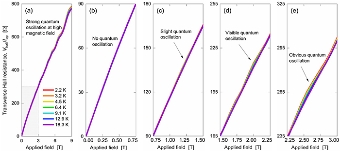
Figure 25. Calibration of an InAs Hall sensor at applied magnetic field of up to 9 T. Quantum oscillation effect is obvious at low temperature and high magnetic field.
Download figure:
Standard image High-resolution image
Figure 26. Photos of (a) a hall sledge on guiding rails, © 2016 IEEE. Reprinted, with permission, from [28]. (b) An 'anti-cryostat' hall probe. Reproduced from [166], with necessary permissions from a contractor of the U.S. Government under Contract No. DE-AC02-06CH11357. Courtesy of ANL managed and operated by UChicago Argonne, LLC. (c) An improved 'anti-cryostat' hall probe measurement approach. Reproduced from [167]. CC BY 3.0. (d) A 3D printed x3yz hall probe. Reproduced with permission from [3].
Download figure:
Standard image High-resolution image4.2.2. Moving/stretched wire method.
The moving/stretched wire method was first proposed by Zangrando and Walker for measuring the field integrals in insertion devices in 1996 [168]. As shown in the schematic in figures 27(a), a stretched copper beryllium (CuBe) wire with certain tension force is placed on the magnetic plane parallel to the undulator axis. By moving the wire by a distance of Δx on the magnetic plane, the integrated voltage Vt refers to the magnetic flux change  and the first vertical field integral is equal to Vt/Δx; by fixing one end of the wire and moving the other end by a distance of Δx on the magnetic plane, the integrated voltage Vt refers to the magnetic flux change
  and the 2nd vertical field integral is equal to VtL/Δx. It should be pointed that the moving/stretched wire method is so far the standard technique for measuring the field integrals in SCUs. The largest uncertainty comes from the mismatch between the magnetic plane and the wire moving plane [163].
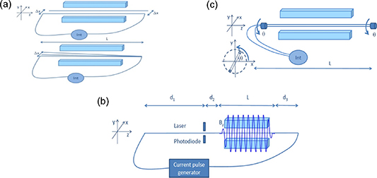
Figure 27. Schematic of (a) moving wire system, (b) pulsed wire system, and (c) rotating coil system. Reproduced from [163]. © IOP Publishing Ltd. All rights reserved.
Download figure:
Standard image High-resolution image4.2.3. Pulsed wire method.
The pulsed wire method was first proposed by Warren in 1988 for measuring the first and second field integrals along the insertion devices [169]. Similar to the moving/stretched wire method, a wire is tensioned along the magnetic axis. When given a current pulse, the wire moves locally due to the undulator field-induced Lorentz forces and this movement propagates as travelling waves. As shown in figure 27(b), the displacement of the wire is detected by a laser and photodiode system. Its value is proportional to the on-axis field, the first field integral and the second field integral when given a positive-negative short pulse current, a short pulse current and a long pulse current, respectively. More details for the calculation can be found in [163]. In 2013, Arbelaez et al developed an algorithm to correct the dispersion and the finite pulse-width errors and reconstructed the 1st field integral successfully in a 10.5-period undulator [170]. A digital signal processing method for correcting the same effects was later proposed by Kasa in 2018 and successfully applied to a 2.4 m long 33 mm-period undulator [171]. Importantly, this pulsed wire method shows great potential in measuring small gap SCUs where hall probe characterization is not feasible.
4.2.4. Rotating coil method.
The rotating coil method was utilized by Doose et al in 2013 to measure the static and dynamic first and second filed integrals as well as multipoles for the first APS superconducting undulator SCU0 [172]. During measurement, the long rectangular coil is aligned to have its central axis coincident with the undulator axis and rotated by two synchronous rotary stages, as shown in figure 27(c). Assuming the long coil is rotated between 0° and 90° or between 180°and 270°, the integrated voltage Vt is equal to the magnetic flux change  and the corresponding first field integral is Vt/Nw, where N is the number of turns in the long coil. By rotating one side of the long coil by 180° at constant angular frequency ω, the second field integral can be obtained [163].
4.2.5. Other methods.
Alternative techniques for measuring the field integrals of SCUs are the vibrating wire method and the stretched wire with direct current method. The concept of vibrating wire was introduced by Temnykh in 1997 [173]: when the wire is fed with an alternating current close to the wire's natural frequency, the wire will excite a unique harmonic in the presence of a magnetic field; by measuring a large number of harmonics, the on-axis undulator field can be reconstructed precisely. The stretched wire with direct current method was introduced for the measurement of BINP SCWs [174]. This method has poor measurement accuracy but with fast measurement speed, allowing for monitoring the field integrals during ramping the current or a quench. More details about the two methods are reported in [163].
4.3. Magnetic field correction
4.3.1. Correction of field integrals.
By optimizing the end coils or end bulk superconductors in a SCU, it is possible to minimize both the first and the second on-axis field integrals to low values numerically. One example is the optimal design of a 10-period staggered-array BHTSU shown in figure 28: the symmetric magnetic structure yields an anti-symmetric on-axis sinusoidal field with default first field integral of zero; by optimizing the sizes of end ReBCO bulks the second field integral can be minimized to an acceptable value [112].
Figure 28. Optimal end design of a 10-period staggered-array BHTSU. Reproduced from [112]. © The Author(s). Published by IOP Publishing Ltd. CC BY 4.0.
Download figure:
Standard image High-resolution imageBut the measurement on-axis field profile always disagrees with the computational result slightly or strongly. It is necessary to utilize additional auxiliary coils to correct the first and second field integrals to ensure the electron bunches follow their original direction of motion without a kick or a displacement. Taking ANL 1.1 m long NbTi planar SCU18-1 for example [27]: correction coils are added at both coil ends to compensate the kick induced by the first field integral, as shown in figure 29(a); a long Helmholtz-like coil wound with ten turns of  0.7 NbTi wire is placed above and below the superconducting coil assembly for compensating the undesired dipole field along the undulator length, as shown in figure 29(b); a pair of dipole coils are installed upstream and downstream of the SCU coil assembly inside the cryostat for compensating the 2nd field integral, as shown in figure 29(c). Similar correction approaches are also applied for the SCUs developed at KIT and LBNL [41, 175]. In conclusion, using these auxiliary coils is a conventional method for correcting the 1st and 2nd field integrals in both PM and SCUs.

Figure 29. (a) Winding scheme of ANL 1.1 m long SCU: blue—main coil, pink—correction coil; (b) Helmholtz-like coil for correcting undesired dipole field along the length; (c) dipole coils installed upstream and downstream of the SCU for correcting the second field integral. Reproduced from [27]. CC BY 4.0.
Download figure:
Standard image High-resolution image4.3.2. Local field shimming.
RMS phase errors below 3° have been achieved on one of the operational SCUs and below 5° have been achieved on FEL SCU prototype. There were no any local magnetic shimming on these devices, but there was mechanical pre-tuning of the magnetic gap. It is important to realize that just precisely machining the magnet cores might not be sufficient to achieve low phase errors. Proper shimming schemes might still be necessary to be developed and applied for correcting the local magnetic fields in SCUs. State-of-the-art shimming approaches for SCUs are summarized as follows,
4.3.2.1. Trim coil and switchable HTS current loops.
The trim coil on poles was first introduced by Prestemon et al for the phase error correction in a Nb3Sn planar SCU prototype, as shown in figure 30(a) [69]. It was shown that the five added NbTi trim coils on poles could provide the perturbation amplitude of >1% at all field levels. Similar shimming approach was later employed by Hwang et al in a 40-pole NbTi planar SCU prototype, showing a peak field of 40 mT (3% of the pole field strength) could be achieved to compensate the phase field error at a particular pole [59]. In 2010, Madur et al experimentally demonstrated that the current direction in a certain trim coil could be adjusted by means of bridge of superconducting heater switches and extended the superconducting bridge concept to control all trim coils [176]. Based on this heater switch concept, Arbelaez et al proposed to use lithographic ReBCO coated conductor for local field correction and numerically studied the possible compensation field provided by the correct current loops [177]. In 2018, Arbelaez et al applied this HTS current loop approach, as shown in figure 30(b), for active correction of local field errors on a full length Nb3Sn undulator developed for LCLS-II project and demonstrated that the RMS phase error could be reduced from 9.2° to 5.4° with this new shimming method [71].

Figure 30. (a) Trim coils on poles. © 2005 IEEE. Reprinted, with permission, from [69]. (b) Heater controlled HTS current loop for field correction. [71] Taylor & Francis Ltd. http://tandfonline.com.
Download figure:
Standard image High-resolution image4.3.2.2. Trim iron pole.
In 2008, Jan et al investigated the feasibility of mounting trim coils and iron pieces directly on the iron poles to correct the local field error in a 40-pole NbTi SCU prototype [178]. It was experimentally demonstrated that local field correction ratio is ∼1.5% after adding 25 mm high iron pieces neglecting the contribution from the trim coils. This trim iron pieces approach was later adopted by Jan et al to correct the local field in a 130-pole SCU prototype, as shown in figure 31(a); the phase error reduced by ∼50% after ΔB/B shimming with iron pieces with proper heights [61]. In 2010, Chunjarean et al proposed a new field correction scheme for SCUs by modifying the iron pole geometry, as shown in figure 31(b); it was experimentally demonstrated that with a slit depth up to 19 mm at pole #21 the associated local on-axis field was reduced by ∼0.15 T while the on-axis field change at the neighboring poles was extremely small; by filling the hollow space with adjustable amounts of iron pieces it was considered possible to minimize the RMS phase errors to extremely low values [179].
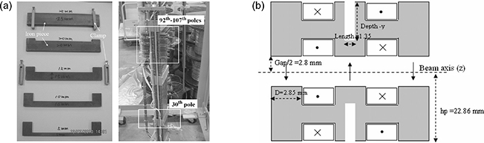
Figure 31. (a) Trim iron pieces with different heights and most of them are clamped to the 92nd–107th poles in the SCU prototype. © 2011 IEEE. Reprinted, with permission, from [61]. (b) Local field correction by modifying the iron geometry. Reproduced from [179]. © IOP Publishing Ltd. All rights reserved.
Download figure:
Standard image High-resolution image4.3.2.3. Induction shimming.
The induction shimming concept for SCUs was first proposed by Wollmann et al [180]. When a superconductive closed loop is installed at the undulator surface and exposed to the change of background field B , it obeys to the Faraday's law of induction
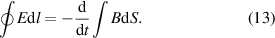
Assuming fully superconducting state is kept in the closed loop during B changes, equation (13) can be reduced to
This means a change of the magnetic flux going through the closed loop is compensated by the magnetic flux induced by the induced currents. Assuming the superconductive closed loop covers a full period, the net flux going through the closed loop tries to stay at zero during SCU ramping and the effective on-axis fields are naturally corrected. Figure 32 describes the idea of using n overlapping closed loops for induction shimming a SCU with n half periods. The feasibility of this phase error correction scheme was later validated through a proof-of-principle experiment [181]. Further experiments by Bernhard et al suffered an unwanted hysteretic effect caused by a part of the shimming loops which reached critical current density and became resistive [182]. We need to keep in mind that equation (14) is a simplified equation which can be incorrect if the HTS closed loop shows obvious flux creep effects ( E-J power law) or saturates earlier during SCU ramping.
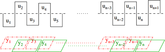
Figure 32. Concept of shimming n half-periods SCU with n overlapping superconductive closed loops. Reproduced from [181]. CC BY 3.0.
Download figure:
Standard image High-resolution image4.3.2.4. Gap adjustment.
The gap adjustment technique was first proposed and adopted for the phase error correction of a 1.5 m long 21 mm period NbTi SCU developed for LCLS-II. The uniformity of the magnetic gap of the full-length SCU was partially controlled by six gap spacers and three gap-adjusting clamps; the phase error was finally minimized to slightly below 5°. The next 1.2 m long SCU18-2 built for the APS storage ring adopted 16 gap spacers and eght clamps for shimming the magnetic gap, as shown in figure 33; the associated RMS phase error was successfully minimized to 2° [159]. Hence, an optimal number of spacers and clamps are essential for a SCU with certain length.
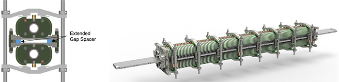
Figure 33. APS SCU18-2 with 16 gap spacers and 8 gap-adjusting clamps for correcting the phase error. Reprinted from [159], Copyright (2018), with permission from Elsevier.
Download figure:
Standard image High-resolution image4.3.2.5. Swapping and sorting.
Recent experiments on staggered-array BHTSU prototypes reached high undulator field at short period length [3, 107], but the field uniformity was quite poor possibly due to the difference of superconducting performances between ReBCO bulks. One possible shimming approach was to first inversely calculating the Je in each ReBCO bulk according to the measured on-axis undulator field and then swapping or sorting the ReBCO bulks shown in figure 34 to minimize the RMS phase error [183].
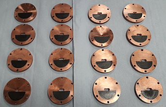
Figure 34. Calculate each ReBCO bulk's superconducting performance and then do swapping or sorting to minimize the RMS phase error.
Download figure:
Standard image High-resolution image4.4. Challenges in HTS technology
In past decades, great efforts towards developing high field accelerator magnets have been made based on the wind-and-react Nb3Sn coil technology [184]. R&D on quadrupole Nb3Sn magnets under the collaboration between CERN and USA has shown great success and this magnet technology will be used in the interaction region in the high luminosity large Hadron collider upgrade [185]. For constructing future high-energy collider, R&D efforts towards developing 16 + T level dipole magnets based on Nb3Sn and HTS technology were continuously made in Europe, USA, and China [186–188]. Very recently, the Nb3Sn technology gained from developing high field accelerator magnets was successfully utilized by LBNL for developing a 1.5 m long SCU prototype for LCLS-II with a period length of 19 mm and an on-axis field of 1.83 T at 8 mm magnetic gap and by ANL for developing a 0.5 m long SCU prototype for APS storage ring with a period length of 18 mm and an on-axis field of 1.2 T at 9.5 mm magnetic gap [71, 72].
However, the HTS technology is not yet ready for application in accelerators or light sources. The first concern is the quench protection of HTS coils whose quench propagation velocity is of the order of cm s−1 (∼100 times lower than LTS), not friendly for quench detection. Non-insulation (NI) ReBCO coil technology is of growing interest recently for itself-quench protection mechanism, however, this technology also has some limitations, which will be discussed below. Very recent experiments on both Bi-2212 Rutherford cable wound racetrack coils and ReBCO CORC cable wound CCT coils showed thermal run-away quenches and timely quench detection and energy extraction [189–191]. Hence, using HTS cables in SCUs could be a good option for fast quench detection and protection, but it needs to be experimentally demonstrated. The second concern is the screening current effects in HTS coils. Unlike multi-filamentary twisted NbTi and Nb3Sn conductors whose magnetization effects are minimized, the transport current in a ReBCO coated conductor is not distributed evenly, for example, during charging a single ReBCO tape slowly the applied transport current always want to shield the tape to reserve the initial zero field as much as possible and thus flows along the edge of the ReBCO tape. This screening current induced field (SCIF) effect has been widely studied in ReBCO coils in NMR and accelerator magnets [192, 193], however, not yet considered in ReBCO coils based undulator in which the SCIF effect can be much more severe due to the much smaller magnetic gap/bore. With regards to ReBCO bulk superconductor, there are also concerns for its application in staggered-array BHTSU, like the Jc variation between individual ReBCO bulks and its brittle ceramic-like property, but these could be overcome by field tunings and pre-stressing techniques.
4.4.1. Screening current effects in HTS undulator.
In this section, we for the first time studied the screening current effects in a VR ReBCO planar SCU by utilizing the critical state model based resistive-adaptive approach proposed by Hashizume et al and further extended by Gu et al in software ANSYS [194, 195]. The critical current density Je in each finite element in the ReBCO tape is a function of the magnetic field and its angle, as shown in equation (8).
In figure 35 is the simulated screening current in a 2D periodical VR ReBCO planar SCU model with 10 mm period length and 4 mm magnetic gap during ramping the operation current Iop linearly from 0 A to 1050 A and then from 1050 A to 0 A. It can be found that the transport current first fills in the ReBCO layers gradually from the edge to the center and its net value gradually drops to zero but with remaining magnetization currents (persistent currents) inside the ReBCO layers. As shown in figure 36, the persistent currents at Iop = 0 A result in an on-axis undulator field of 0.48 T instead of nearly zero in the NbTi SCU. By alternating the operation current Iop, a hysteresis loop of the on-axis undulator field taking into account the screening current effect is obtained and plotted in figure 37. This can be a good reference for guiding the operation of ReBCO coil-based SCUs, which are of potential interests to the future application in synchrotrons and FELs. But it should be noted that there can be a slight change of the hysteresis loop and a slight decay of the on-axis undulator field when taking into account the E-J power law based flux creep effects in ReBCO coated conductors.

Figure 35. Current distribution in 2D periodical VR ReBCO planar SCU during charging the operation current Iop linearly: 0 A–1050 A–0 A.
Download figure:
Standard image High-resolution image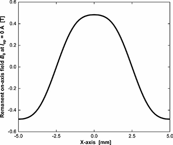
Figure 36. Remanent on-axis field B0 at Iop = 0 A.
Download figure:
Standard image High-resolution image
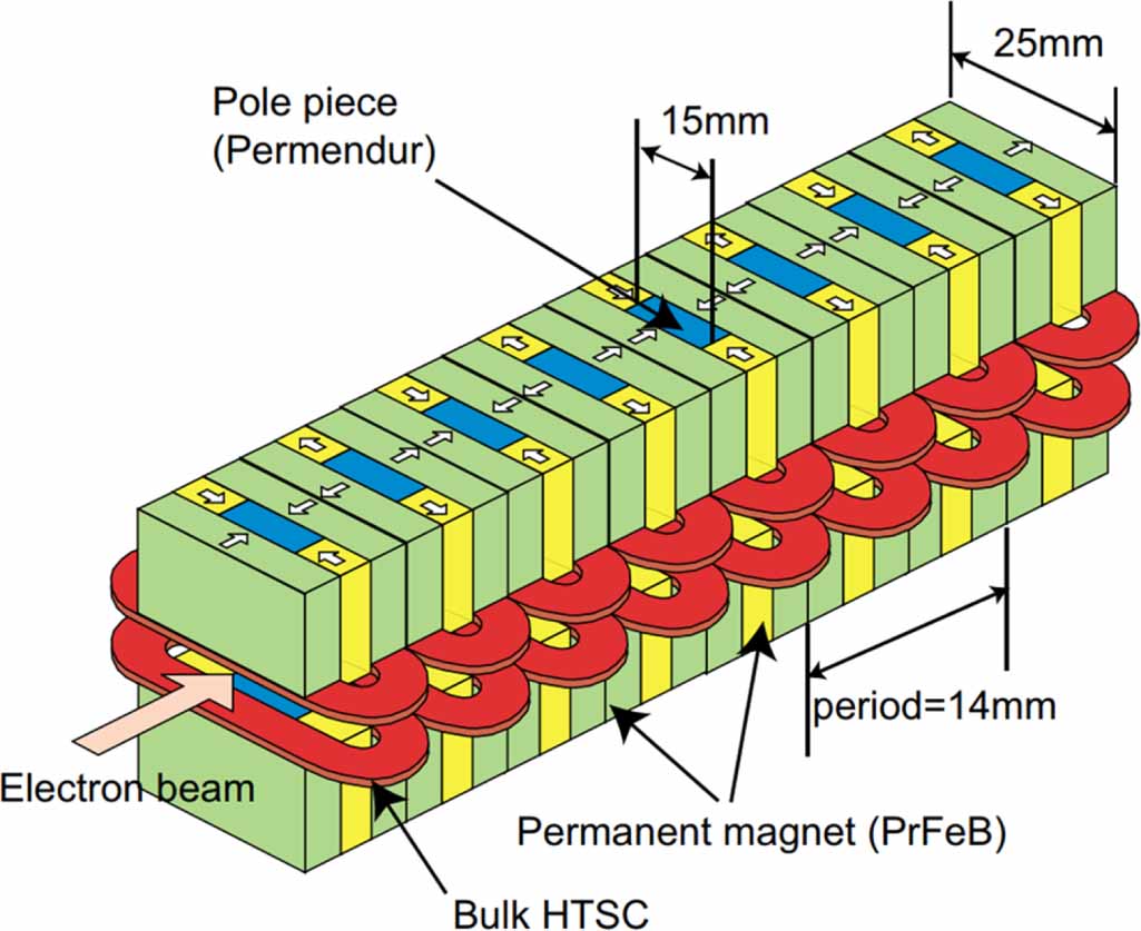
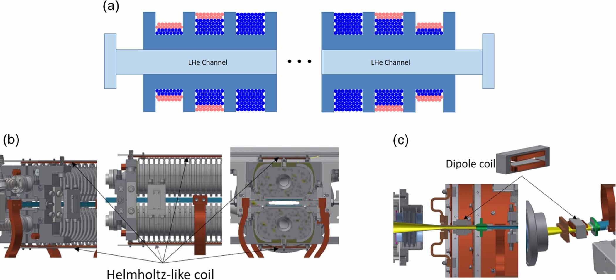
Figure 37. Hysteresis loop of on-axis field B0 after taking into account the screening current effect.
Download figure:
Standard image High-resolution image
4.4.2. Non- and partial-insulation technology in HTS undulator.
NI HTS coil technology was first proposed by Hahn et al [196] and became a hot research topic later for two main reasons: a) more compact and better thermal stability—the elimination of insulation layers can enhance the overall coil current density and the radial thermal conductivity in the HTS coils; b) self-quench protection mechanism—the NI-HTS coil can survive when the transport current Iop exceeds the critical current Ic because a certain amount of current will bypass its original superconducting spiral path through turn-to-turn contact and the equivalent decay time constant decreases with the rise of apparent coil resistant represented by both Rr and Rθ . However, the NI-HTS coil often has an obvious charge or discharge delay, for example, the central magnetic field needs longer time to stabilize after charging the coils. The PI HTS technology by insulating the HTS coils every several layers is a potential solution to speed up the charge–discharge rate while retain the self-quench protection characteristic in the meantime [197].
Experiments on NI-HTS undulator was first reported by Kesgin et al showing stable steady-state operation and long field decay time due to the current sharing between interlayers [81]. Further experiments on a continuously wound HTS undulator proved the PI-HTS undulator could reach a maximum Je level of 2.1 kA mm−2 at 4.2 K and its field profile agreed well with simulations, indicating the current flowed along the spiral path; the PI-HTS undulator could be charged much faster but requiring much shorter time for stabilizing in comparison to the NI-HTS technology [74].
To conclude, an insulation layer enclosing several HTS tapes is quite similar to an 'HTS cable' which often results in a thermal run-away quench. The PI technology is extremely promising for application in ReBCO coils based SCUs.
5. Conclusions and prospects
NbTi SCUs, with either planar or helical type, have now reached impressive performances at the KIT synchrotron and APS storage rings, demonstrating reliable operation without quenches or with stable electron beams in case of a quench. It was also experimentally demonstrated that a SCU could obtain higher on-axis field B0 than an ideal CPMU with the same geometry, showing outperformed photon flux in the high energy part of the x-ray spectrum. One can also buy NbTi SCUs from industry now as for ANSTO who has a contract with Noell GmbH. The wind-and-react Nb3Sn technology has been developed for decades and utilized for developing SCU prototypes successfully in USA. Most probably, next breaking news is the beam commissioning of Nb3Sn undulator in APS storage ring. In the past decade, several HTS undulator prototypes wound with 2G ReBCO coated conductors were made world-wide but none of them reached a practical level of undulator field. Open questions like the screening current effects and the NI technology remained to be answered. Very recent R&D on staggered-array bulk ReBCO undulator at PSI/Cambridge obtained an on-axis field B0 of as high as 1.54 T @ 10 K at 10 mm short period and 4 mm magnetic gap, showing great potential for its application in FELs and DLSRs where small magnetic gap is allowed. But it should be mentioned that the on-axis field uniformity is quite poor at the moment and remained to be improved with the help of precisely machined industrial bulk HTSU samples and the new shrink-fit assembly technique. The comparison of theory limits between different types of SCUs and CPMUs provides the undulator designer with helpful tips on selecting proper SCU design approach with given restrictions, for example the period length and the effective K-value. It can be found that the Nb3Sn/ReBCO helical and the bulk ReBCO planar undulators show outstanding performances than the others at period length as short as 10 mm. But their mechanical feasibility, like the allowed winding radius for Nb3Sn wire and ReBCO coated conductor, is not evaluated and its critical analysis is left to the reader. Other technical challenges including the SCU cryostat design, the magnetic field measurement and the magnetic field correction have been reviewed in detail. The pulsed wire method shows great potential in measuring small gap SCUs where hall probe scanning is not easy. In addition, how to conduct local field shimming is still an open question to the SCU community even though the NbTi based SCU devices successfully operated at the KIT synchrotron and APS storage ring did not require local magnetic shimming.
State-of-the-art commissioned SCUs in storage rings have two separated vacuums for the SCU coil assembly and the vacuum chamber to thermally isolate the superconducting coils. The minimum difference between the vacuum gap and the magnetic gap is 1 mm in SCUs developed for the KIT synchrotron. This gap difference could be further minimized with in-vacuum SCU design in which a thin copper conducting sheet of ∼0.2 mm instead of a separate vacuum chamber, similar to that of in-vacuum PM undulator, is utilized to absorb the heat load. The in-vacuum SCU concept is of growing interest to low-repetition FELs where ultra-high vacuum is not mandatory as for synchrotrons and the resistive wall wakefields induced heat load is limited. For high-repetition (≫kHz) FELs, the use of in-vacuum SCUs could still be feasible using a large liquid helium cryo-plant (large cooling power at 2 or 4 K) for cooling the whole beamline efficiently instead of GM cryocoolers for each undulator module. For reaching the same K-value, the minimized magnetic-mechanical gap difference allows for shortening the period length, thus reducing both the LINAC energy and the length of the total undulator beamline. To conclude, R&D on SCUs with tunable K-value up to ∼2 and period length as short as possible is of continuing interest world-wide for either reducing the total costs or enhancing the photon energy; R&D on variably polarized SCU, for example the SCAPE, is another hot research topic for both synchrotrons and FELs.
Data availability statement
All data that support the findings of this study are included within the article (and any supplementary files).
Acknowledgments
This work is supported by the Swiss Accelerator Research and Technology (CHART) program, www.chart.ch. The authors would like to thank Thomas Schmidt from Paul Scherrer Institute, Sara Casalbuoni from European XFEL, Cristian Boffo from Fermi National Accelerator Laboratory, Efim Gluskin from Argonne National Laboratory, Qiaogen Zhou from Shanghai Advanced Research Institute, Fusan Chen and Yuhui Li from Institute of High Energy of Physics, Beijing, and Ryota Kinjo from Kyoto University for their helpful advices on improving this review work.