


Abstract
Raman spectroscopy is frequently used to study the properties of epitaxial graphene grown on silicon carbide (SiC). In this work, we present a confocal micro-Raman study of epitaxial graphene on SiC(0001) in top-down geometry, i.e. in a geometry where both the primary laser light beam as well as the back-scattered light is guided through the SiC substrate. Compared to the conventional top-up configuration, in which confocal micro-Raman spectra are measured from the air side, we observe a significant intensity enhancement in top-down configuration, indicating that most of the Raman-scattered light is emitted into the SiC substrate. The intensity enhancement is explained in terms of dipole radiation at a dielectric surface. The new technique opens the possibility to probe graphene layers in devices where the graphene layer is covered by non-transparent materials. We demonstrate this by measuring gate-modulated Raman spectra of a top-gated epitaxial graphene field effect device. Moreover, we show that these measurements enable us to disentangle the effects of strain and charge on the positions of the prominent Raman lines in epitaxial graphene on SiC.
Export citation and abstract BibTeX RIS

Content from this work may be used under the terms of the Creative Commons Attribution 3.0 licence. Any further distribution of this work must maintain attribution to the author(s) and the title of the work, journal citation and DOI.
1. Introduction
Since the first experimental characterization of its unconventional properties [1, 2], graphene has been a focus for many researchers. Epitaxial graphene (EG) on silicon carbide (SiC) [3–5] is of particular interest because it offers the possibility for large scale production [6] suitable for the development of electronic devices such as, e.g. high frequency transistors [7]. Next to electrical characterization of EG by electronic (magneto-)transport measurements, Raman spectroscopy plays an important role because it provides crucial information on, e.g., the number of layers, defects, doping, strain and the so-called buffer layer [6, 8–23]. Raman spectroscopy is non-destructive and therefore can be used to characterize devices made from graphene. However, unlike the case of exfoliated graphene devices, where usually a bottom gate is realized with the aid of the silicon substrate, the application of Raman spectroscopy to EG devices is not straight forward. This is because the latter mainly rely on top gates where a suitable dielectric and gate metal are deposited on top of the graphene. Note that a bottom-gate can be realized for EG on SiC as well [24], but this requires rather complicated processing using ion implantation which is not readily available to many researchers. Hence, in EG devices, the graphene layer in the gated region is buried by the gate structure and in the region of the contact pads by a metal. However, EG resides on an optically transparent substrate and therefore should be accessible to Raman spectroscopy when probed from the backside as shown in figure 1(a). In this work we describe top-down Raman measurements through the SiC substrate using a confocal micro-Raman setup. Contrary to the expectation, the top-down geometry leads to an increased Raman signal from the graphene layer which will be explained below. In addition, we demonstrate how this measurement geometry can be applied for disentangling the effects of charge and strain on the position of the prominent Raman lines.
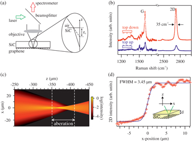
Figure 1. (a) Setup used for confocal Raman spectroscopy in top-down configuration. Light is focused through the SiC substrate on the graphene layer. The sketch on the right side depicts the refraction at the air/SiC interface. (b) Raman spectra of MLG measured in top-up and top-down configuration (50 × objective with NA = 0.55, SiC thickness ≈370 μm). The spectra are offset from each other for clarity. (c) Ray tracing analysis of the beam profile of light focused into the SiC demonstrating aberration caused by refraction at the air/SiC interface. The dashed lines mark the spread of the focal points due to aberration. (d) Two-dimensional (2D) line intensity profile obtained by scanning over a graphene edge in top-down configuration. The solid line shows a fit using the error function which results in a focus width of 3.5 μm.
Download figure:
Standard image High-resolution image2. Experimental aspects
Epitaxial monolayer graphene (MLG) was grown on semi-insulating 6H-SiC(0001) substrates (II–VI Inc.). The Si-face had a chemo-mechanical (CMP) polish and was etched in hydrogen prior to the growth of graphene. The back side of the samples (C-face) had an optical polish with an rms roughness of 1.5 nm as determined by atomic force microscopy. Graphene was grown by annealing in an argon atmosphere [6] using a custom built, automated growth reactor [25]. Quasi-free standing monolayer graphene (QFMLG) was obtained by intercalation of the buffer layer with molecular hydrogen [16, 26]. Using QFMLG we prepared a top-gated graphene field effect transistor (GFET) with silicon nitride (SiN) as a gate dielectric [27–29]. The SiN layer was grown by plasma-enhanced chemical vapor deposition as described in [27].
Micro-Raman spectra were recorded at room temperature in confocal back scattering geometry with a Jobin Yvon T64000 spectrometer using a frequency doubled Nd:YVO4 laser (λ = 532 nm). In order to focus through the 370 μm thick SiC substrate, we used an objective with a long working distance and a numerical aperture of NA = 0.55. The setup is shown in figure 1(a). Contamination of uncovered graphene layers and reflection of light by the sample support were avoided by placing the samples on spacers or—in case of top-gated structures—in a dedicated setup where the sample was fixed at its edges. The Raman signal of the SiC substrate was removed from the spectra by subtracting a reference spectrum obtained from clean SiC not covered with graphene as introduced in [9].
3. Results and discussion
3.1. Enhanced collection efficiency of the top-down geometry
Figure 1(b) displays Raman spectra of a graphene sample (SiC thickness 370 μm) recorded in both, top-up and top-down geometry using the objective with NA = 0.55. Compared to the conventional top-up geometry, the signal intensity is significantly enhanced in the top-down geometry, i.e. when measuring through the SiC substrate. This observation is valid for both, the graphene and the buffer layer [23] components. Note, that the intensity in the D band region is primarily due to the Raman signal of the buffer layer [23] and only the small narrow peak at approximately 1360 cm−1 is induced by defects in the graphene layer. The enhancement factor amounts to approximately 3.8 and 4.7 for the G and 2D band, respectively. The peak positions and peak widths are independent of the measurement geometry. Any contribution to the spectra of graphene layers possibly grown on the carbon face of the SiC substrate can be excluded.
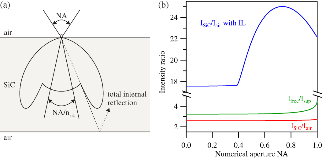
At first glance, the observation of this intensity enhancement is puzzling as one would expect that the observed Raman signal in top-down configuration is lowered by reflection and refraction of the incident and scattered light at the air/SiC interface. The refraction causes aberration because rays originating from the outer part of the objective lens are focused deeper in the SiC than rays close to the optical axis as shown in figure 1(a). The aberration increases with the nominal focal depth z0 and the numerical aperture NA of the objective used for the experiment. In order to demonstrate this, we show in figure 1(c) a raytracing analysis using a Gaussian beam profile. The nominal focal depth z0 = −135 μm was obtained experimentally by a z-scan in top-down geometry through the sample. The numerical aperture was NA = 0.55 and the index of refraction of SiC was set to 2.6. The two dashed lines at nSiCz0 = −351 μm and at  indicate the distances with respect to the illuminated SiC surface where rays from close to and far away from the optical axis meet, respectively. Note the logarithmic intensity scale. It can be seen that a focal width of the order of a few micrometers is feasible. This result was verified experimentally. To that end, we determined the width of the focus by scanning the laser beam in top-down geometry over a graphene edge as shown in figure 1(d). The width of the focus is evident from the increase of the 2D line intensity as the graphene edge is moving through the laser beam. A fit with the error function yields a focus width of 3.5 μm under optimized conditions. Therefore, aberration plays a minor role for the combination of substrate and objective used in this work. Consequently, the effective numerical aperture in top-down configuration can be described by NA/nSiC which causes a decrease of the solid angle of detection by 86%. Therefore, a mechanism should exist which overrides these effects. The only plausible explanation is that more Raman scattered light is emitted into the SiC substrate than toward air.
The experimental findings are explained by considering the theory of dipole radiation at a dielectric surface. In the classical view of Raman scattering, the oscillating electric field of the incident light induces a time dependent polarization in the graphene layer. The susceptibility, defining the polarization, is modulated by lattice vibrations of the graphene layer and the resulting time dependent polarization gives rise to dipole radiation with frequencies of the elastic and Raman scattered light. However, the emission pattern of a radiating dipole is changed compared to the emission in free space, if it is located close to a dielectric surface [30]. In general, more light is emitted into the material with a higher refractive index. This effect was previously exploited in fluorescence spectroscopy [31] and is nowadays used for single-photon collection from single emitters [32].
Figure 2(a) shows the calculated emission pattern of an ensemble of dipoles located at the interface between SiC and air with the dipoles being oriented parallel to the surface. The calculation, which was performed using a formalism developed by Lukosz [30], immediately illustrates that most of the light is emitted into the SiC substrate. Integration over the two half-spaces shows that about 96% of the light is emitted into the SiC substrate. The detectable intensity is obtained by integration over the solid angle of detection which is a function of the numerical aperture NA. The result is shown in figure 2(b) which plots the calculated ratio between the intensities expected in top-down (ISiC) and top-up (Iair) geometry as a function of NA. For our case of NA = 0.55 this leads to a theoretical enhancement of 2.6. Considering the reflection loss of the incident and outgoing Raman scattered light at the SiC/air interface if measuring through the substrate, a theoretical value of the enhancement factor of 1.7 is expected, which is lower than our observed value of around 4. This indicates that the formalism used for estimating the enhancement does not capture all the details. This is also apparent from the experimentally observed difference in the enhancement of the 2D and G lines. Taking into account the wave length dependence of the refractive index of SiC, we arrive at negligible differences in the estimated enhancement factors for the two bands. Obviously more work (especially theory) is required to develop a model that accounts for all the observations. This, however, is beyond the scope of this paper.
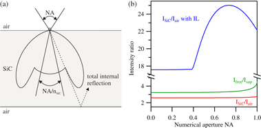
Figure 2. (a) Calculated emission pattern of parallel oriented dipoles directly located on the SiC surface. The solid angle of detection in top-down and top-up configuration is depicted for NA = 0.55. The dashed line marks the critical angle of total internal reflection. (b) Calculated intensity ratio between top-down and top-up configuration (ISiC/Iair) as a function of numerical aperture NA without and with an immersion lens (IL). Ifree/Isup is the intensity ratio between free-standing graphene and graphene supported by SiC, both measured in top-up configuration.
Download figure:
Standard image High-resolution imageFigure 2(b) also shows that the intensity ratio ISiC/Iair hardly changes with the value of NA. It varies only between 2.6 and 2.7 because the regions of high intensity beyond the critical angle of internal reflection (see figure 2(a)) can not be detected. On the other hand, if the refraction of light at the SiC/air interface is eliminated by, e.g. using an immersion lens, an enhancement factor of up to 25 could be expected (see figure 2(b)).
The strong asymmetry in the emission pattern also explains the observed enhancement of the Raman intensity of free-standing EG [33, 34] which was prepared by locally removing the SiC substrate. Shivaraman et al [33] and Waldmann et al [34] observed that the G band intensity is enhanced by a factor of approximately two and five compared to measurements of SiC supported regions, respectively. In the case of the free-standing regions, the index of refraction is the same on both sides of the graphene, leading to a symmetric intensity distribution. The intensity ratio between free-standing graphene and supported graphene in top-up configuration Ifree/Isup is also included in figure 2(b). For NA = 0.9, which was used by Waldmann et al [34] an enhancement of 3.5 is expected which agrees well with the observation. Unfortunately, Shivaraman et al [33] do not state the NA of the objective lens. However, as seen from our calculations, the enhancement factor varies only slightly with NA (between 3.3 and 4.5).
3.2. Disentangling the effect of strain and charge on the position of Raman signals of epitaxial graphene
As shown in the preceding section, Raman spectroscopy in top-down configuration through the SiC substrate can effectively be applied for the study of EG. In the following, we make use of this for disentangling the effect of strain and charge on the position of Raman signals of EG. This is an important question, because the charge carrier concentration of graphene is often estimated by Raman spectroscopy, referring to measurements of Das et al [20] who measured the dependence of the G line and the 2D line position on the charge carrier density of exfoliated graphene on SiO2/Si. Exfoliated graphene is typically free of strain but in EG on SiC both strain and charge affect the position of Raman signals.
In order to better understand the role of charge and strain on the Raman signals of EG on SiC we have studied how the position of the G and 2D line depends on the carrier concentration in a top-gated quasi-free standing EG transistor. The SiN gate dielectric used in the present study has recently been shown to induce an additional electron doping of the graphene layer [27]. Hence, the intrinsic p-type doping of QFMLG (p ≈ 6 × 1012 cm−2) was converted by the SiN layer into n-type doping (n ≈ 4 × 1012 cm−2). Using moderate gate voltages, the device could be gated beyond the charge neutrality point.
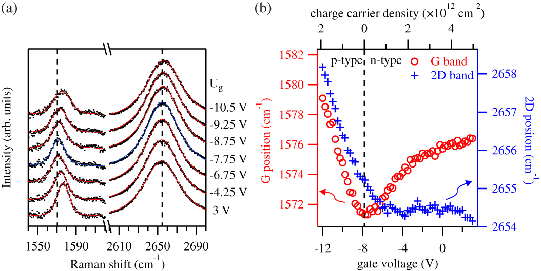
Figure 3(a) displays a selection of Raman spectra measured on a top-gated GFET made from QFMLG under various applied gate voltages. In figure 3(b) the gate voltage dependent positions of the G and 2D band are plotted, which were obtained by fitting single Lorentzians to the individual spectra. The top axis of figure 3(b) indicates the charge carrier concentration, which was determined by Hall effect measurements prior to the Raman measurements. For a gate voltage of 3 V the electron concentration amounts to 5 × 1012 cm−2. Charge neutrality is reached at a gate voltage of −7.8 V. More negative gate voltages induce hole conduction. Finally, at a gate voltage of −12 V, a carrier concentration of 2 × 1012 cm−2 is obtained.
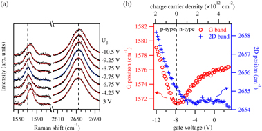
Figure 3. (a) Selection of Raman spectra measured on a GFET made from QFMLG under various applied gate voltages. Solid lines represent the fitting result with single Lorentzians. The spectrum with the blue fitting curve corresponds to charge neutrality with the position of the G and 2D mode marked by dashed lines. (b) Gate voltage dependence of the G and 2D band position of the EG transistor. The dashed line indicates charge neutrality. The top axis gives the charge carrier concentration which was determined by Hall effect measurements prior to the Raman measurements.
Download figure:
Standard image High-resolution imageStarting from the highest hole concentration, the G band frequency softens with decreasing hole density until a minimum is reached at charge neutrality. Then, for increasing electron concentration a hardening of the G band frequency is observed. However, the magnitude of the slope of the curve is smaller than for holes and decreases with increasing n. This observation is in line with other experimental reports [20, 35] which have used a polymer electrolyte or a back gate, respectively, for controlling the carrier type and density. Very recently, Tiberj et al [38] studied the reversible optical doping of graphene by illuminating flakes on SiO2 with different laser fluences. They observed that the G and 2D lines are shifted with illumination intensity and argued that this shifts were caused by variations of the chemical equilibrium between graphene, the substrate, and the atmosphere. Although they could not directly derive the charge carrier density, their data show the same qualitative behavior as ours shown in figure 3(b). The behavior of the carrier density dependent G line position was explained in the theoretical work by Lazzeri and Mauri [39]. They demonstrated that the asymmetric behavior of the G band with respect to charge neutrality results from adding the symmetric, dynamic contribution caused by the Kohn anomaly to the monotonously decreasing contribution of the adiabatic processes.
The 2D band shows a different behavior. Starting from the highest hole concentration, the 2D line position decreases when the hole density is lowered. After passing the charge neutrality point, a further slight decrease of the 2D line position is observed. At electron concentrations higher than 2 × 1012 cm−2, the position of the 2D line stays more or less constant. These observations are qualitatively in agreement with the results of Das et al [20] and of Tiberj et al [38]. Das et al compared their data to calculations based on the adiabatic approximation. They argued that dynamic effects due to the Kohn anomaly play a negligible role and explained the discrepancies between experiment and theory by experimental limitations. Our measurements suggest that dynamic effects should not be neglected completely. We also note that Araujo et al [35] observed that the 2D line softens with increasing carrier concentration independent of the carrier type which is in contrast to the data presented here and in the other experimental studies [20, 38].
The effects of strain and charge on the positions of the Raman lines are best seen when plotting the 2D band position as a function of the G line position as shown in figure 4 for the data set of figure 3(b). At this point, only doping effects are important because the strain is not changed by the gate voltage. Effects by strain cause an overall shift which is discussed later on. As seen from figure 4, the data points can be divided into two branches. Each branch shows an approximately linear behavior. The slopes of these lines thereby depend on the carrier type and amount to mchp = 0.37 ± 0.01 and mchn = −0.08 ± 0.01 for holes and electrons, respectively.
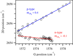
Figure 4. 2D line position as a function of the G band position with variation of the doping level (data of figure 3(b)).
Download figure:
Standard image High-resolution imageIf we evaluate the data of Das et al [20] in the same manner, we obtain a somewhat different result. In the range of the charge carrier concentrations discussed here, the data of Das et al [20] exhibit a slope of 0.2 for p-type doping whereas for n-type doping the slope is close to zero. Both values have to be taken with care because of a large scatter of the data points which are scarce in the region of carrier concentration considered here. A similar evaluation of the measurements presented by Tiberj et al [38] yields slopes of 0.6 and −0.2 for the p- and n-type regions, respectively. Note that Tiberj et al [38] do not give explicit values for the charge carrier density. The measurements of Araujo et al [35] on bottom-gated graphene on SiO2/Si reveal a slope of −1 for both, n- and p-type doping. However, in contrast to our work and the studies of Das et al [20] and Tiberj et al [38], they observed a softening of the 2D line when the Fermi level was gated away from the Dirac point. The discrepancies between these measurements imply that it is difficult to determine the charge carrier density of graphene by Raman spectroscopic measurements unless the specific system has been thoroughly characterized. At this point we have to mention that after device fabrication our graphene exhibits a spectral integrated D/G ratio of about one. The Raman spectra of Das et al [20] indicate the absence of a defect induced D band, whereas in the work of Araujo et al [35] the possible presence of a D band is not mentioned. In both cases, the charge carrier concentration was not measured but calculated from the gate voltage assuming a certain capacitance. In principle, however, the relation between the 2D line position and the G line position should be independent of how the charge carrier concentration is determined.
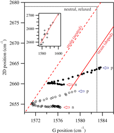
Next we consider the effect of strain by discussing figure 5. The open circles in that figure represent the data already shown in figure 4. The closed circles are measurements made on a different spot in the same device. As with the previous data set, the data points fall on two branches, one representing n-type QFMLG, the other one p-type QFMLG. Note that p-type branches run parallel to each other indicating that the averaged slope of mchp = 0.38 ± 0.02 is universal for p-type graphene. The same holds for the n-type branches and its slope of mchn = −0.11 ± 0.03. The only difference between the data sets is that they converge for zero charge density toward different values of the G and 2D line position. The difference between these positions can only be caused by different strain as explained in the following.
Figure 5. 2D line position as a function of the G line position measured on two different positions of a GFET (circles) and for a variety of QFMLG samples with different stain and amount of p-type doping (inset). Open circles represent data of figure 4. The solid line is a fit to the data shown in the inset. The dashed line represents the strain dependence of the 2D and G band positions for neutral graphene. The vertical/horizontal dotted line marks the position of the G line/2D line for unstrained and uncharged graphene taken from the literature [40, 41].
Download figure:
Standard image High-resolution image
In addition to the gated measurements of the GFET we have included in the inset of figure 5, as crosses, measurements for a variety of QFMLG samples. There is obviously a large scatter caused by different amounts of strain and charge. Nevertheless, the positions of the data points suggest that they follow a general trend. QFMLG is p-type doped with a charge carrier concentration of a few 1012 cm−2 (see [16, 26]). Hence doping induced variations cannot account for the large variations and we can assume that the general trend is due to variations in strain. If a straight line is fitted to the data points, we obtain the solid red line shown in figure 5 and as well in the inset, which has a slope of mstr = 2 ± 0.2. That value is in good agreement with previous estimates [16, 36, 37]. The dashed line in figure 5 is obtained by shifting the solid line describing the strain dependence onto the neutral positions measured in our GFET. Obviously, that line with mstr ≈ 2 describes the relation between the positions of the 2D and G band of neutral graphene. Furthermore, if we take the G band position for unstrained and uncharged graphene of 1583 cm−1 as determined by Reich and Thomsen [40], we find from our relation a 2D line position for unstrained and uncharged graphene of 2679 cm−1, which matches the value for unstrained exfoliated graphene reported by Graf et al [41].
With the knowledge developed above it is now possible to trace back the shifts of the 2D and G lines caused by strain and charge of an arbitrary quasi-free standing EG sample. The only additional information necessary is the knowledge of the charge carrier type (electrons or holes). The shifts caused by charge (ch) and strain (str) can be calculated using the relations
and

where ΔG and Δ2D are the differences between the measured and the neutral, relaxed G and 2D position which can be taken from [40, 41]. The corresponding shifts of the 2D band due to charge and strain are given by Δ2Dchp/n = mchp/n·ΔGchp/n and Δ2Dstr = mstr·ΔGstr.
4. Conclusion
In this work we have demonstrated the possibility to probe EG layers by Raman spectroscopy in a top-down geometry, i.e. through its SiC substrate. We observed an unexpected increase in collection efficiency and explained it in terms of dipole radiation at a dielectric surface. The fact, that most scattered light of the graphene layer is emitted into the higher refractive index material provides important input to the field of Raman spectroscopy of graphene and is not only limited to EG on SiC because in general graphene has to reside on a substrate. In addition to the enhanced collection efficiency, the method opens possibilities to study graphene by Raman spectroscopy even if the surface is covered by non-transparent materials such as gate stacks or metal contacts.
Using the top-down configuration we have investigated the doping dependence of the G line and 2D line position of QFMLG in a GFET. We have determined the relation between the positions of these lines in dependence of the charge density and type as well as its variation with strain. This knowledge can be used to evaluate strain and charge in arbitrary (quasi-free standing) EG samples from Raman spectroscopy. The only additional input needed is the charge carrier type, information that can easily be deduced from other measurements such as x-ray induced photoelectron spectroscopy (XPS).
In addition, as discussed above, the dependence of the 2D line position on the charge carrier concentration appears to be poorly described by calculations performed within the adiabatic approximation. We propose that this phenomenon be studied by state-of-the-art theory including effects caused by the Kohn anomaly as was previously done for the G line [39].
Acknowledgment
This work was supported by the European Union within the project ConceptGraphene (grant agreement number 257829) and by the DFG in the framework of the project ULTRA-Graphene (project identifier SE 1087/7-1).