


Abstract
We examine the predictive capabilities of first-principles theoretical methods to calculate the phonon- and impurity-limited electron mobilities for a number of technologically relevant two-dimensional materials in comparison to experiment. The studied systems include perfect graphene, graphane, germanane and MoS2, as well as graphene with vacancies, and hydrogen, gold, and platinum adsorbates. We find good agreement with experiments for the mobilities of graphene (μ = 2 × 105 cm2 V−1s−1) and graphane (μ = 166 cm2 V−1s−1) at room temperature. For monolayer MoS2 we obtain μ = 225 cm2 V−1s−1. This value is higher than what is observed experimentally (0.5–200 cm2 V−1s−1) but is on the same order of magnitude as other recent theoretical results. For bulk MoS2 we obtain μ = 48 cm2 V−1s−1. We obtain a very high mobility of 18 200 cm2 V−1s−1 for single-layer germanane. The calculated reduction in mobility from the different impurities compares well to measurements where experimental data are available, demonstrating that the proposed method has good predictive capabilities and can be very useful for validation and materials design.
Export citation and abstract BibTeX RIS

Content from this work may be used under the terms of the Creative Commons Attribution 3.0 licence. Any further distribution of this work must maintain attribution to the author(s) and the title of the work, journal citation and DOI.
1. Introduction
Ever since the advent of graphene [1], effort has greatly intensified to discover new kinds of two-dimensional (2D) materials with intrinsic properties that will make them ideal for electronic applications [2]. Of special interest are their transport properties, in particular their electronic mobilities that can, for example, in suspended graphene reach hundreds of thousands of cm2 V−1s−1, although external influences such as substrates, impurities, and contacts make it hard to reach that limit [3]. These prospects have not only triggered considerable effort in the research of non-graphene 2D material, but have moved the question of their ideal electronic and transport properties, as well as their potential to perform at or close to their theoretical limit, into a central position. For that, a well-validated, parameter-free method that can predict the limiting carrier mobilities for the ideal material, as well as the effect of external influences, would be highly desirable in order to assess the real-life usability of novel and existing 2D materials, decide how much a certain device structure, contact or substrate influences their 'natural' conductivity, and explore and design novel materials that have specific desired properties. In this paper, we discuss such a method that has been recently proposed to be applicable to 2D materials for germanane [4], a germanium-based graphane analogue, and apply it to a number of other 2D test systems, including graphene with and without impurities, graphane, and MoS2 (single-layer and bulk limits), for which we examine the predictive powers in light of the available experimental results. The good predictive capabilities of this method that we find, in combination with the fact that no idealized or ad hoc materials properties have to be used as is common in most all other methods, opens the prospect of targeted 2D design, as well as providing a tool that allows (indirect) structure validation from the transport and optical properties in cases where direct imaging of the synthesized 2D material is difficult.
2. Theoretical method
Mobility is a key quantity in electronic transport since it describes how the motion of a charge carrier is affected by an applied bias. Conventional mobility models usually suppress atomic-scale detail when treating two-dimensional or thin-layer semiconductor systems, using effective mass theory [5] or bulk energy bands to calculate the kinetic energy of electrons [6]. After that, the main scattering mechanisms that limit mobilities, which are due to phonons and ionized impurities [7], are often treated similarly. Until recently, calculations of electron–phonon scattering rates have relied on empirical deformation potentials and rigid pseudo-ion models [8–10]. Large differences among empirical deformation potentials have been found in the literature [11], and only recent theoretical advances have begun to produce deformation potentials calculated with first-principles methods that may clarify this situation [12]. The comparison of several numerical approaches to calculate electron–phonon scattering rates at high energies reported in [9] illustrates the complexity of the problem.
With the emergence of two-dimensional materials that consist only of surfaces and thus show strong effects from environmental effects and adsorbates, predictive parameter-free theoretical methods for the calculation of carrier mobilities that take into account quantum mechanical effects at the atomic level have become a necessity. Here, we apply a first-principles method that we have developed for 3D semiconductor materials to calculate mobilities limited by phonon and ionized impurity scattering to a selection of 2D materials [13]. We will refer to this approach in the following as the ab initio mobility (AIM) method.
Our approach is based on the linearized Boltzmann equation in the relaxation time approximation. Ground state calculations were performed within the Quantum ESPRESSO [14] software package using the local density approximation (LDA) [15] for exchange and correlation functionals unless otherwise indicated. Several key quantities such as wave functions, eigenenergies and electron–phonon coupling constants are extracted from this package. To calculate the mobility we use [16].

where nc is the density of carriers,  is the momentum relaxation time for electrons in state
  ,
,  their group velocity, and
  the Fermi–Dirac distribution.
In order to determine  for the case of scattering of electrons due to phonons, we use Fermi's Golden Rule,
where g is the electron–phonon coupling function,  are the Fermi–Dirac occupation factors,
  the band energies,
  the phonon frequencies, and
  is the Bose–Einstein distribution function. The derivation of equation (2) (see [16]) considers both scattering of an electron from state k to k + q and also backscattering from k + q to k by either emission or absorption of phonons. The electron–phonon coupling matrix element g is given by
where M is the atom mass,  are phonon polarization vectors,
  represent atom displacements with periodicity
  , relative to their equilibrium positions,
  and
and  is the screened one-electron potential. The interatomic force constants and phonon frequencies are determined by density functional perturbation theory [17], as implemented in the Quantum ESPRESSO package. The normalization with respect to the number of ions is already included in the wave functions and thus does not appear explicitly in equation (3). Ab initio calculations of spectral functions α2F(ω), which are directly proportional to the electron–phonon coupling g, compare well with experiment [17], providing both a direct test of the validity of the calculated g, and an indirect test of the accuracy of the Kohn–Sham orbitals used in these calculations.
The Coulomb scattering rate for impurities and defects is calculated as [16].

where  is the volume of the macrocrystal, and θ is the angle between
  and
and  . Within the Born approximation, the scattering matrix
  is given by
  where the self-consistent scattering potential
  is the difference between the potential of a reference 'unperturbed' system and the potential of the system in the presence of a defect or impurity. We have included screening of the scattering potential as described in [13] in the Debye parameterization, where the screening length is proportional to the inverse square root of the electronic density. All the integrals over k-space have been evaluated using the tetrahedron method [18].
Table 1. Calculated phonon and impurity limited mobility compared with experiment.
| Phonon-limited mobility (cm2 V−1s−1) | ||
|---|---|---|
| Calculated | Experiment | |
| Graphene | 2 × 10⁵ | 1.2 × 10⁵ |
| Graphane | 166 | 150 |
| Germanane | 18195 | |
| MoS2 (monolayer) | 225 | 0.5–200 |
| MoS2 (bulk) | 47.9 | 15 |
| Impurity-limited graphene mobility at N = 1012 defects | ||
| Au adatom | 3169 | 2801 |
| Pt adatom | 150198 | 409514 |
| Vacancy | 950 | |
| Hydrogen | 34295 | |
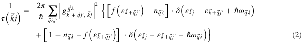
Figure 1. Graphane band structure, calculated within PBE.
Download figure:
Standard image High-resolution image
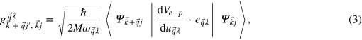
Figure 2. Self-consistent electronic charge density of a graphene monolayer with an Au adatom left of the center.
Download figure:
Standard image High-resolution image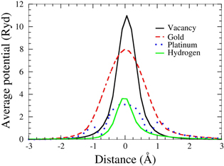
Figure 3. Self-consistent scattering potentials for different impurities in graphene as labeled. Au and Pt are adatoms, while H passivates the C pz orbitals.
Download figure:
Standard image High-resolution image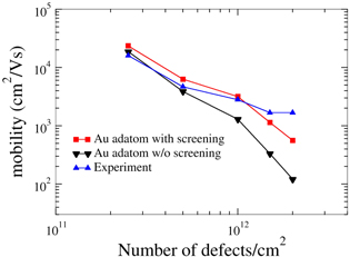
Figure 4. Electron mobility due to impurity scattering as a function of Au adatom concentration on graphene compared with experiment [29] (T = 18 K).
Download figure:
Standard image High-resolution image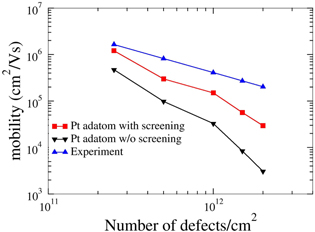
Figure 5. Electron mobility due to impurity scattering as a function of number of Pt adatom concentration on graphene compared with experiment [30] (T = 18 K).
Download figure:
Standard image High-resolution imageThe method used here has been applied successfully to bulk semiconductors in the past, where good agreement was found for the case of silicon [13] (the room temperature phonon-limited electronic mobility was calculated to be 1900 cm2 V−1s−1 versus an experimental value of 1500 cm2 V−1s−1) and also for diamond [19] (the calculated value is 130 cm2 V−1s−1 while the experimental value [20] is between 100 and 660 cm2 V−1s−1, with more recent values closer to the lower end). Also, a very recent adaption of our method by others [21] and an expansion that uses Monte Carlo transport simulations instead of the relaxation time approximation for MoS2 give results very similar to ours, supporting the use of the computationally much easier and more efficient relaxation time approximation used here.
3. Results and discussion
In this paper, we will examine a series of widely studied materials for which either accepted experimental mobilities have been established, or for which questions exist that require theoretical calculations that are not based on experimental parameters. These include the 'suspended' mobility limit in graphene, graphane, and in MoS2; the question of whether the electron mobility in single-layer MoS2 beats that of bulk MoS2; and how a full quantum-mechanical treatment of the effect of impurities on the mobility compares with available experiments.
Due to the high environmental sensitivity of 2D materials and the difficulty in ensuring and monitoring the material and its surroundings, a full exploration of the electronic properties of a wider range of 2D materials under full control of geometric and environmental conditions is currently only possible from the theoretical side, i.e. by calculation. Since these calculations do not include any free parameters, they can be used to predict the potential of new 2D materials for the optimization of future electronic devices. Our results are summarized in table 1 in comparison to the experiment and will be discussed in detail in the following.
- (a)Suspended graphene and graphane Since the zero-band gap of graphene limits its use to applications that do not require a band gap, hydrogenated graphene [22] (graphane, figure 1), which is a semiconductor with a theoretical band gap of 5.4 eV [23], has recently received more attention. This material has also attracted a lot of interest for its possible applications in hydrogen storage. The measured electron mobility of 150 cm2 V−1s−1 for graphane on a SiO2/Si substrate [24] is several orders of magnitude lower than that of graphene, and to date it is not clear if graphane suffers from similarly detrimental effects of the substrate on the carrier mobility as graphene does, where suspended graphene has a conductivity that is at least 1–2 orders of magnitude larger than that of graphene on a substrate. However, since one may expect that hydrogen 'protects' the in-plane carbon bonds better from substrate effects than is the case in graphene, it would be conceivable that graphane is closer to its theoretical limit than graphene, which we will investigate here.For single-layer graphene we obtain a mobility of 200 000 cm2 V−1s−1. This is in reasonable agreement with mobility measurements of free-standing graphene (up to 120 000 cm2 V−1s−1) and with previous predictions [24, 25]. Thinking in terms of effective masses, this is consistent with the fact that the carrier mass in the Dirac cone around the pseudo-gap is very small, with a value of 0.012 free electron masses (me) [26].However, this situation is very different for graphane. There, we obtain a PBE [27] direct band gap at the Γ point of 3.46 eV and a conduction effective mass of 1 me (figure 1). Due to the fact that PBE underestimates band gap values, as has been shown for graphene previously where the hybrid HSE06 functional finds a value of 5.4 eV [23], we don't expect a perfect agreement with experiments for the band gap. On the other hand, effective masses are usually well reproduced by traditional DFT. The relatively high effective mass in graphane thus indicates a much lower electron mobility than in graphene, which is indeed the case. We calculate for perfect, suspended graphane an electron mobility of 166 cm2 V−1s−1. This is in excellent agreement with the experimental value of 150 cm2 V−1s−1 [28], which is little disputed. Thus, we find sensible results for perfect 2D carbon films within the AIM approach, which especially predicts that substrates have a small to negligible effect on the electron mobility in graphane, in contrast to graphene.
- (b)Graphene with adsorbed impurities: the importance of screening To further compare with experimental data, we have performed impurity-limited graphene mobility calculations for platinum and gold adatoms, for which experimental values are available [29, 30]. Au and Pt adatoms both have their minimum-energy position in the center of a graphene ring, 2.37 and 1.82 Å above the graphene plane, respectively. In addition, we also examine vacancies as well as dilute hydrogen passivating the pz orbital of a C atom, in order to examine the effect of point defects as well as the mobility in slightly hydrogenated graphene.The typical changes in the electronic charge density when adding an impurity—here Au—are shown in figure 2. Figure 3 shows the radially averaged scattering potentials generated by these changes. The vacancy and the Au-adatom potentials have the greatest impact on scattering while the potentials for Pt adatoms and hydrogenated C atoms are about half as large. As shown in figures 4–5 in the case of the Au and Pt adatom impurities, we find that the inclusion of screening leads to a much better agreement with available experimental data from McCreary et al [29] and Pi et al [30], respectively. At 1012 defects per cm2, we obtain mobilities of 3200 (figure 4), 150 200 (figure 5), 950 (figure 6), and 34 300 (figure 7) cm2 V−1s−1 for Au, Pt, vacancies and H impurities, respectively. As expected, the larger mobilities are given by the smaller potentials (Pt and H) while the smaller mobilities correspond to the larger potentials of Au and vacancies. These calculations represent the first fully quantum mechanical and parameter free predictions of mobilities from impurity, and demonstrate in comparison to experimental values the significant influence of screening on the mobility.
- (c)Novel non-carbon materials: MoS2 and germananeAmong the newly discovered 2D materials, single-layer (SL) MoS2 has been of particular interest due to its intrinsic band gap, which enables its use in conventional transistor structures for electronic switching, and also due to the suggested prospect of enhancing its air-based carrier mobility (proposed to be in the single-digit numbers) to ∼200 cm2 V−1s−1 by dielectric engineering, e.g. within a HfO2/SL-MoS2/SiO2 structure [31]. However, an alternative explanation may be that the latter measurement simply involved a structure and SL-MoS2 material that allowed electron conduction closer to the 'perfect' limit, which we will examine within the current work. Also, the suggested use of multi-layer instead of SL MoS2 to facilitate device fabrication [31] has opened up the question for a more detailed study of the mobility of the multi-layer limit, i.e. bulk MoS2, where the SL-MoS2 sheets are held together by van der Waals forces.The MoS2 monolayer has a PBE direct band gap of 1.8 eV and a conduction effective mass of 0.5 (figure 8). Bulk MoS2 has an indirect PBE band gap of 0.95 eV and a conduction effective mass of 0.62 (figure 9), which is in good agreement with previous theoretical simulations [32]. For single layer MoS2 the experimental mobility values ranges from 0.5–3 cm2 V−1s−1 in recent studies [33, 34], much lower than the originally measured values of 100–260 obtained by Fivaz et al [35]. More recently a value of 200 cm2 V−1s−1 was achieved by Radisavljev et al [31]. Our calculated value of 225 cm2 V−1s−1 gives a very reasonable upper bound to these measurements, while the sensitivity to external effects that we demonstrated for graphene may explain why much lower values over a wide range have also been measured. Other very recent theoretical efforts have found values for single-layer MoS2 of 130 cm2 V−1s−1 (potentially up to 320 cm2 V−1s−1 due to numerical uncertainties) [36] by using a combination of density functional calculations with Monte Carlo simulations and a value of 410 cm2 V−1s−1 [37] by using first-principles to obtain acoustic and optical deformation potentials and the Fröhlich interaction, both in the same range as our result, but most possibly with larger uncertainties and computational efforts. For bulk MoS2 we obtain an electronic mobility of 48 cm2 V−1s−1 which is higher than the experimentally reported mobility of 15 cm2 V−1s−1 [38].Very recently, another type of 2D semiconductor named germanane has been realized, where [111] sheets of bulk germanium are terminated by varying functional groups such as H [4] or CH3 [39]. Of these two we studied hydrogenated germanane (GeH), with which we obtain a direct band gap of 1.56 eV at the Γ point for an isolated layer using the hybrid HSE06 exchange–correlation function [40–42], which typically calculates band gaps in close agreement with experimental values, which in the case of germanane is 1.59 eV [4]. The calculated effective mass at the conduction band at Γ is 0.09 me. This low effective mass leads to a high mobility of 18 200 cm2 V−1s−1 for single-layer germanane [4], probably making it the (non-zero band-gap) semiconductor with the highest electron mobility.
4. Conclusions
In this work, we have used first-principles methods to calculate the electron mobilities for the technologically relevant two-dimensional materials graphene, graphane, MoS2, and germanane. Our phonon-limited results for graphene, graphane and single-layer MoS2 compare favorably with experiments. We find that graphane seems to be much more insensitive to substrates than graphene, which we rationalize by the protecting effect of the H-atoms on the conducting C-layer. For bulk MoS2 the theoretical value (48 cm2 V−1s−1) is about three times larger than the measured one, but is still considerably smaller than the SL value. Our findings for single-layer MoS2 are supported by other recent theoretical results that give values of the same order of magnitude as reported here, but should be computationally more efficient and thus more widely applicable. Finally, AIM predicts a mobility of 18 200 cm2 V−1s−1 for the recently synthesized germanane, which would thus be the fastest of all semiconductors with non-zero band gap.

Figure 6. Electron mobility due to impurity scattering as a function of vacancy concentration in graphene (T = 18 K).
Download figure:
Standard image High-resolution image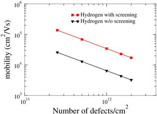
Figure 7. Electron mobility due to hydrogen impurity scattering as a function of number of defects (T = 18 K).
Download figure:
Standard image High-resolution image
Figure 8. Monolayer MoS2 band structure, calculated within PBE.
Download figure:
Standard image High-resolution image
Figure 9. Bulk MoS2 band structure, calculated within PBE.
Download figure:
Standard image High-resolution image
We further investigated the effect of impurities on the electronic mobility of graphene, which previously has only been done within the model of idealized Coulomb scatterers, and not within a fully quantum mechanical scattering approach. We find good agreement with experiments in the case of Au and Pt adatoms. We also give predictions for the cases of hydrogen and vacancy scattering. We find that the detrimental effect on the mobility is notably smaller for Pt and H than for Au and vacancies. We also find that screening proves to be a crucial factor when calculating impurity-limited electronic mobilities. The overall magnitude of the impurity results, which are significantly smaller than the phonon-limit, shows that extrinsic effects should typically dominate conduction in graphene. It also shows that a theory such as the present AIM approach, which allows the introduction of scattering from impurities that are present in the environment, is indispensable; this provides a much more realistic comparison with available experiments. Our present study has thus shown that the AIM approach yields reasonable ab initio predictions for electron mobilities, and provides unique opportunities for exploratory work to computationally discover and design new 2D materials with the desired properties.
Acknowledgments
This research was funded by the Center for Emergent Materials at The Ohio State University, an NSF MRSEC (Grant No. DMR-1420451). We also thank the Ohio Supercomputer Center for support under Project Nos. PAS0072 and PAA0010.