


Abstract
There is an ongoing debate regarding the mechanism of swift heavy ion (SHI) track formation in CaF2. The objective of this study is to shed light on this important topic using a range of complementary experimental techniques. Evidence of the threshold for ion track formation being below 3 keV nm−1 is provided by both transmission electron microscopy (TEM) and Rutherford backscattering spectroscopy in the channelling mode, which has direct consequences for the validity of models describing the response of CaF2 to SHI irradiation. Furthermore, information about the elemental composition within the ion tracks is obtained using scanning TEM, electron energy loss spectroscopy, and with respect to the stoichiometry of the materials surface by in situ time of flight elastic recoil detection analysis. Advances in the analyses of the experimental data presented here pave the way for a better understanding of the ion track formation.
Export citation and abstract BibTeX RIS

Original content from this work may be used under the terms of the Creative Commons Attribution 3.0 licence. Any further distribution of this work must maintain attribution to the author(s) and the title of the work, journal citation and DOI.
1. Introduction
Material modification using swift heavy ions (SHIs) having a mass above 15 atomic mass units (amu), and a specific kinetic energy above 0.1 MeV amu−1 is an important contemporary research topic [1–6] with diverse applications like hadron therapy, radiation waste storage and track etched membrane production. Irradiation with SHI generates intense electronic excitation along its trajectory because at these kinetic energies (10–2000 MeV) the dominant channel for energy dissipation is via numerous collisions with electrons in the material. The density of deposited energy, usually expressed in terms of the SHI's electronic stopping power (keV nm–1), is often quite sufficient to produce permanent damage along the ion trajectory (i.e. ion track) or activate various thermally driven processes enabling patterning or synthesis of nano-structured materials [4, 7–10].
Interactions of individual SHIs with crystalline materials can result in the formation of ion tracks in the bulk [3, 11–13], accompanied by surface features (nano-hillocks, nano-craters and similar) that can be found at the SHI impact site by means of atomic force microscopy (AFM) [2, 5, 14–18]. Despite their nanometric sizes, ion tracks in the bulk can be observed with several techniques. The most often used techniques are transmission electron microscopy (TEM) and Rutherford backscattering spectroscopy in the channelling mode (RBS/c) [12, 14, 19–21]. TEM offers the possibility for direct observation of the individual ion tracks, while the RBS/c measures the ion track size indirectly by observing the fraction of disordered material in the crystal matrix, as a function of the applied SHI fluence. With some exceptions, the agreement in measured ion track radii between these two techniques is very good [20].
Due to the so-called velocity effect, slower ions (E/A < 2 MeV amu−1 are much more efficient at ion track formation than the faster ones (E/A > 8 MeV amu−1, even when both have the same electronic stopping power [11, 21, 22]. Two most widely used models of ion track formation, namely the inelastic thermal spike model (ITSM) and the analytical thermal spike model (ATSM), attribute the velocity effect to two completely different physical mechanisms. In the case of the ITSM, the velocity effect (i.e. reduction in track sizes at high SHI velocities) is related to the low density of the deposited energy due to the high energy of scattered electrons (primary or delta electrons) [12, 20]. This results in a monotonically increasing threshold for ion track formation with ion velocity, i.e. E/A. On the other hand, the ATSM attributes larger track sizes at low SHI velocities (below 2 MeV amu−1) to a contribution from the Coulomb explosion and this is considered as an important difference between those two models [23, 24].
Due to the existence of the velocity effect, medium sized accelerators can provide important complementary data at energies below 1 MeV amu−1 which are not easily accessible to large accelerators. In particular, the threshold for ion track formation constitutes an important experimental quantity (often needed for testing various ion-solid interaction models) that can be in many cases easily accessible to medium sized accelerators [1, 9, 11, 16, 19, 25, 26]. Similar to ion tracks in the bulk, there is always a threshold for nanohillock formation on the surface. Above the threshold, nanohillocks typically grow in size with increasing ion energy. Similar values for the threshold for ion tracks in the bulk and for nanohillocks on the surface have often been observed [5, 6], thus enabling us to characterise the threshold with different techniques.
1.1. Ion tracks in CaF2: current status
At present, a hotly debated topic is the formation mechanism of ion tracks in CaF2 and closely related to this, the nature of the velocity effect (even its very existence) in this material [26–31]. A still incomplete body of experimental data available for analysis is the main reason why this debate is ongoing. Despite extensive experimental work done previously [32–35] where ion tracks in CaF2 were investigated by TEM, only recently one experimental study using RBS/c was published [27]. As noted by Szenes [28], this RBS/c data (along with XRD data from the same work) indicate the absence of the velocity effect in the 1–11 MeV amu−1 range. In response [29], TEM data was used as a proof for existence of the velocity effect in CaF2 because very small ion tracks were found indicating a threshold for track formation around 20 keV nm−1 after GeV monoatomic irradiation, while a lower threshold around 10 keV nm−1 was found after MeV cluster ion irradiation. Not surprisingly, even the newest experimental results on AFM observation of SHI induced nanohillocks on CaF2 surfaces were used in this discussion [30].
The explanations given by the two models about the rather small track sizes observed in CaF2 are radically different and at present seen as a test of their validity [27–29]. According to the ITSM, the small track sizes observed by TEM are caused by strong ionic bonding that prevents amorphization within the ion track [27]. Therefore in CaF2, and probably other non-amorphizable materials, ion tracks consisting of strongly disordered material are considered as a result of the quench of the boiling phase that occurs along the SHI trajectory. Melting, on the other hand, is seen as requirement for CaF2 modification as observed by RBS/c and XRD, as well as previous swelling studies [36, 37]. For this reason, the track radii measured by different methods are not always the same, and consequently the thresholds also vary. Based on the thermodynamic parameters for CaF2, the amount of energy necessary to induce a molten phase is around 0.6 eV atom–1 [30] and for the formation of the vapour phase around 1.7 eV atom–1 [27] is required. For very low velocity SHI, in the ITSM this corresponds to stopping powers of 2.6 keV nm−1 [30] and 7.4 keV nm−1, respectively.
The problem of small ion track sizes in CaF2 is solved within the ATSM in an altogether different way. Since large track sizes observed in other materials after irradiation with SHIs with low velocity are interpreted as contribution of a Coulomb explosion, small track sizes in CaF2 are seen as evidence of its absence [28, 38]. Therefore, a pure thermal spike is thought to be at the origin of ion track formation in CaF2, and in this later case all experimental data can be described using model parameters for the high velocity regime (i.e. a0 = 4.5 nm, g = 0.18), yielding a threshold at 9.5 keV nm−1 [31]. Recently, this threshold was corrected by Szenes to 7 keV nm−1 to accommodate newer RBS/c results, while the TEM data from [34, 35] were dismissed as erroneous [28]. Material melting remains as a necessary condition for ion track formation, while the boiling criterion is considered as unrealistic [28], although it is also possible to describe all TEM data available in the literature by applying the boiling criterion within the ATSM and taking the velocity effect into account [26].
Finally, there is also an open question about the atomic structure within the ion track. Based on previous investigations on the response of CaF2 to electron beams [39], the characteristic intermittent track structure observed by TEM is believed to consist of faceted anion voids [32–35, 40]. These voids can be viewed as calcium inclusions that should be easily formed due to the small misfit between the fcc structure of the Ca sublattice and CaF2. Then, the much lower density of the calcium with respect to CaF2 would give rise to contrast as seen in TEM [33]. However, the fate of the fluorine gas liberated from within the ion track remains unknown: it might remain trapped within the CaF2 crystal but outside the ion tracks [40] or it might be released by diffusion from the ion track [35].
1.2. Ion tracks in CaF2: motivation for the present work
The aim of the present work is to resolve the dilemma outlined above by providing much needed additional experimental data. First, we observe that the TEM data of tracks in CaF2 due to irradiation with monoatomic projectiles [34, 35] show an unexpectedly uniform behaviour throughout the intermediate and high velocity range of the SHI (E/A = 2–11 MeV amu−1). Similarly, RBS/c data [27] show the same uniform behaviour in almost the same range of energies (E/A = 1–11 MeV amu−1), as observed earlier by Szenes [28]. These observations led us to formulate the hypothesis that the velocity effect in CaF2 (as conceived in the ATSM) is shifted to lower values of E/A below 1 MeV amu−1. A smaller shift has been observed previously [41], but recently a larger shift has been observed for tracks produced by lighter SHIs like oxygen [9].
To test our hypothesis, we have undertaken SHI irradiation of CaF2 using monoatomic heavy ions with a specific kinetic energy E/A = 0.1–0.2 MeV amu−1, followed by an investigation of the resulting ion tracks using TEM, RBS/c, AFM and time of flight elastic recoil detection analysis (ToF-ERDA). The SHI beams used in this study cover precisely the range of interest, i.e. electronic stopping powers between 3–7 keV nm−1. Furthermore, in the present case the irradiation conditions match almost exactly the ones used in [30] because iodine and xenon ions at these energies are practically indistinguishable projectiles, hence the comparison between bulk and surface tracks in CaF2 becomes possible. Thus, experimental data obtained here complements the existing data: in this energy range there is hitherto no RBS/c data, and available TEM data was obtained after MeV cluster ion irradiation, which could bear additional effects due to extreme values of deposited energy densities [40, 42, 43] although opinions are divided on this topic [27, 41]. This complementarity should enable us to establish the threshold for ion track formation in the bulk CaF2, and to finally resolve the ardent controversy about the velocity effect in this material. Last but not least, to shed some light on the inner track structure, i.e. its elemental composition, both ToF-ERDA and scanning TEM–electron energy loss spectroscopy (STEM–EELS) were performed in our current study.
2. Experimental details
Single crystalline CaF2 (111) samples of 7 × 7 mm2 were prepared by cleaving from single crystal piece (Crystec) before the irradiation. Additionally, several TEM grids containing CaF2 crystal grains were prepared by crushing CaF2 into a mortar followed by dispersion into ethanol and dripping the dispersion onto a TEM grid provided with a carbon membrane.
All SHI irradiations were performed at the Ruđer Bošković Institute (RBI) using 6 MV EN Van de Graaff accelerator. Iodine ions with energies of 10, 15 and 23 MeV were used in both normal and grazing incidence geometry. Single crystal samples irradiated at normal incidence were oriented with a small tilt angle (6°) with respect to the surface normal, in order to avoid possible SHI channelling. The SHI beam was scanned to ensure homogenous irradiation and the fluence was measured by observing the ion flux in the Faraday cup before and after the exposure. For longer exposures, the irradiation was interrupted a few times to ensure that the ion flux was stable. A full list of all irradiation parameters is given in table 1.
Table 1. Irradiation parameters used in this work calculated using the SRIM code [44]: electronic stopping power dEe/dx, nuclear stopping power dEn/dx and projected ion range R.
| SHI | dEe/dx (keV nm−1) | dEn/dx (keV nm−1) | R (μm) |
|---|---|---|---|
| 10 MeV I5+ | 2.93 | 0.63 | 3.29 |
| 15 MeV I6+ | 4.27 | 0.47 | 4.47 |
| 23 MeV I6+ | 6.26 | 0.35 | 5.87 |
| 2 MeV Li2+ | 0.72 | 0.001 | 3.82 |
| 1 MeV H+ | 0.005 | 0.00 004 | 11.99 |
Ion tracks in the bulk were characterised using RBS/c and TEM. The samples were analysed by TEM before and after irradiation with SHI using a JEOL 200CX electron microscope operated at 200 kV acceleration voltage at room temperature. In order to further understand the processes induced by heavy ion irradiation but also by electron irradiation during the TEM investigation, the sample irradiated at 23 MeV was analysed by STEM–EELS technique. We were using the JEM ARM 200F electron microscope corrected for spherical aberration in the STEM mode. The microscope was operated at 200 kV, while the sample was maintained at room temperature during observation.
For the RBS/c analysis, a 2 MeV Li2+ and 1 MeV H+ beams delivered by the 1 MV Tandetron accelerator were used (RBI). The samples were mounted on a goniometer and angular scan maps (tilt, azimuth) were performed for target alignment. The beam spot size was 1 mm in diameter and the ion current was kept at about 1 to 2 nA. To detect the backscattered ions, a silicon surface barrier detector with a thickness of 300 μm and bearing 3 mm slits was positioned at 160° with respect to the probing beam direction.
Ion tracks on the surface were analysed using tapping mode AFM and in situ ToF-ERDA. The AFM measurements were performed under ambient conditions using a Dimension 3100 AFM and Nanosensors NCHR cantilevers at Universität Duisburg-Essen. Images were analysed using the WSxM code [45]. The ToF-ERDA measurements (RBI) were performed using a 23 MeV I beam at 1° grazing incidence angle with respect to the sample surface. The ToF-ERDA spectrometer [46, 47] was positioned at an angle of 37.5° towards the beam direction (RBI). All data were collected in the 'list mode' and offline replay/analysis with sections was performed using the Potku software package [48].
3. Experimental results
3.1. TEM results
Here we present evidence of ion track formation for all SHI irradiation energies used. The TEM clearly revealed ion tracks produced by stopping power as low as 2.9 keV nm−1, with the well-known intermittent morphology.
3.1.1. Before irradiation
At low TEM magnification the CaF2 grains proved to be beam resistant. Working for several minutes in such low-beam illumination conditions did not induce any visible modifications at the morphological or structural level. However, after a few tens of seconds of e-beam irradiation under a focused e-beam, CaF2 started to decompose, followed by Ca oxidation as shown in figure 1. One can observe in the following pictures that after exposing the crystal grain to a focused electron beam, it starts to modify both morphologically (as one can see in the TEM images, figure 1(c)) and structurally (see the selected area electron diffraction (SAED) patterns at the beginning of the TEM observation and after ca. 1 min of observation under the focused beam, figures 1(d) and (e)). Diffuse diffraction rings appear in the SAED patterns along with the CaF2 spots. The diffraction rings indicate the in situ formation of CaO (cubic phase). In order to avoid the rapid beam-induced structural modifications, we have chosen to work at low magnification using the diffraction contrast for the track studies.

Figure 1. The TEM image (a) and corresponding SAED pattern (b) of a CaF2 grain close to the [−112] zone axis at the beginning of observation at low magnification (low e-beam fluence). The TEM image (c) and corresponding SAED pattern (d) of the same CaF2 grain after ca. 60 s of observation under focused e-beam (high e-beam fluence); (e) SAED pattern of the same crystal grain in a different orientation (close to the [111] zone axis) after ca. 120 s of observation under focused e-beam (high e-beam dose).
Download figure:
Standard image High-resolution image3.1.2. After irradiation with iodine ions at 23 MeV
For all analysed samples, the SHI irradiation effects could only be revealed for high values of objective lens defocus, either underfocus (df < 0) or overfocus (df > 0). To be able to correctly interpret the TEM images we note that for the TEM images obtained in the diffraction contrast mode, the features exhibiting bright Fresnel fringe correspond to regions in the sample with lower density than the surrounding matrix (voids). The contrast is opposite when the objective lens is overfocused, the image then showing a dark Fresnel fringe on the side of the lower-density material.
The SHI irradiation effects were most visible in the case of the sample irradiated at the highest energy of 23 MeV. When observing the irradiated crystal grains in no-tilt or slightly tilted orientation, the underfocused images exhibit doublets of bright dots of 2–3 nm size (figure 2). The separation distance between the two bright dots differs across one crystal grain, being smaller close to the grain border and larger for the pairs of dots inside the grain away from the grain border. We attribute these pairs of bright spots to the extremities of the irradiation tracks crossing the crystal grain and intercepting the two limiting surfaces (bottom and upper surface). The variation of the separation distance with the location of the bright dots goes in line with the thickness increase of the analyzed wedge-shaped grains. The SHI tracks consist of heavily disordered material regions which, according to the mentioned Fresnel contrast criterion, correspond to regions of lower density within the matrix (figure 2).
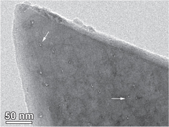
Figure 2. SHI induced nanofeatures revealed as pairs of bright spots on the CaF2 crystal grain.
Download figure:
Standard image High-resolution imageIn order to get a side view of the irradiation tracks, the sample was tilted inside the microscope up to 40 degrees with respect to the electron beam. The TEM images obtained in underfocus and overfocus conditions then reveal a certain structuring of the irradiation tracks along their trajectory. They show a contrast modulation with 2–4 maxima along their length.
The prolonged observation in the TEM of the SHI irradiated sample leads to the formation of two kinds of defects apart from the irradiation tracks. These defects have already been reported in literature as defects induced by e-beam irradiation during the TEM observation: (i) on one hand aggregated defects (voids) sometimes organised in periodic arrays and (ii) dislocation loops located in the (111) planes.
The through focus contrast behaviour of the first type of defects proves that they are nanovoids of up to 10 nm size. They are indicated by white arrows in figures 3 and 4 in underfocus and overfocus condition. It is known from the literature [49, 50] that these nanovoids tend to organise, with the increase of the irradiation dose and the observation time, into a cubic superlattice oriented parallel to the cubic CaF2 lattice. In our case, due to the low fluence observation conditions and the early stage observation during imaging, the induced nanovoids are not yet organised into a superstructure.

Figure 3. Under-focus (a) and over-focus (b) TEM images reveal low density material inside the irradiation tracks represented by the white and, respectively, the black dots. White arrows point to electron beam-induced voids.
Download figure:
Standard image High-resolution image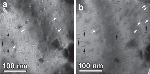
Figure 4. Underfocused (a) and overfocused (b) TEM image of a tilted CaF2 grain containing 23 MeV I irradiation tracks (black arrows) and an array of electron beam-induced voids (white arrows).
Download figure:
Standard image High-resolution imageThe second type of e-beam induced defects are the dislocation loops bordering planar defects. The calcite grain in figure 5 is oriented close to the [1–10] zone axis (see the inserted SAED pattern). The image in figure 5(a) was acquired in the first seconds of observation, therefore only the irradiation tracks are visible as doublets of white spots. After a few minutes of observation, pairs of planar defects bordered by dislocation loops started to appear under the influence of the e-beam. By comparing with the corresponding SAED pattern, one can notice that these planar defects are situated in the {111} crystallographic plane of CaF2. Such defects have been also mentioned in literature [2].

Figure 5. (a) Wedge-shaped CaF2 grain oriented close to the [1–10] zone axis (corresponding SAED pattern inserted) containing 23 MeV I irradiation tracks imaged as doublets of white dots; (b) e-beam induced planar defects grouped in pairs, bordered by dislocation loops (seen edge-on).
Download figure:
Standard image High-resolution image3.1.3. After irradiation with iodine ions at 15 MeV
Similar SHI track features were observed on the samples irradiated at 15 MeV. The bright scattered dots in figure 6(a) represent end-on irradiation tracks with a similar size (2–3 nm) as in the case of the sample irradiated at 23 MeV. The side view of the irradiation tracks (figure 6(b)) reveals their fine structure of 3–4 aligned nanovoids of 3–4 nm size. E-beam induced faceted nanovoids of up to 8 nm size can also be observed after a few tens of seconds of observation.

Figure 6. (a) Under-focused TEM image showing end-on 15 MeV I irradiation tracks revealed as white dots (black arrows); (b) side view of the irradiation tracks (black arrow) in a grain that was tilted with respect to the electron beam in the microscope. The white arrow points to the regular in situ e-beam induced nanovoids.
Download figure:
Standard image High-resolution image3.1.4. After irradiation with iodine ions at 10 MeV
Similar SHI induced track effects were observed on the samples irradiated at 10 MeV. Groups of up to 5 bright dots aligned parallel to the vertical direction in figure 7(a) represent irradiation tracks in side view orientation, consisting in nanovoids of 5–6 nm size. After a few tens of seconds of observation, e-beam induced defects can be noticed as faceted nanovoids of up to 8–9 nm size (white arrows in figure 7(b)).
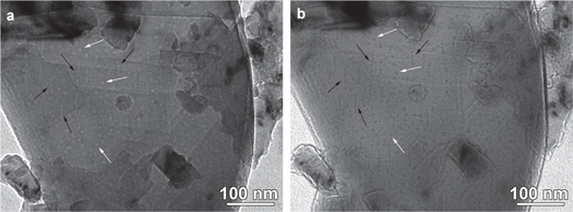
Figure 7. Under-focused (a) and overfocused (b) TEM images showing 10 MeV I irradiation tracks revealed as groups of 4–5 white dots (black dots when overfocused) aligned parallel to the vertical direction (pointed by black arrows); the white arrows indicate nanovoids induced by e-beam irradiation during the observation in the TEM.
Download figure:
Standard image High-resolution image3.2. In situ TEM results
Detailed inspection of the ion tracks for prolonged time and under the various TEM conditions indicated difficulties in obtaining reliable information about ion track sizes. On a careful examination of the ion tracks in the sample irradiated at low energy (10 MeV I), we observed that, apart from the already mentioned defects induced by the e-beam, there is a certain morphological evolution of the ion tracks themselves under the electron beam. We noticed that, although initially not visible, the irradiation tracks are only revealed after a few tens of seconds of observation under the e-beam, inside grains which at first apparently contained no ion tracks. The images in figure 8 are taken from the same CaF2 grain at different moments starting from the beginning of the observation in the microscope. The image recorded during the very first seconds of observation in underfocus condition does not exhibit any visible ion track (figure 8(a)). Without changing the illumination conditions or defocus of the objective lens, the ion tracks started to become visible after about 30 s of observation, while after 2 min they showed quite well defined shapes.

Figure 8. TEM image of a CaF2 grains irradiated at 10 MeV: (a) at the beginning of the TEM observation, underfocused image; (b) after 3 min of TEM observation, underfocused image.
Download figure:
Standard image High-resolution imageIn figure 8(b) we present the TEM image after 3 min of observation, at the same defocus condition as in figure 8(a) (recorded directly after imaging started). The irradiation tracks are now clearly visible, showing the morphological features described previously. We mention that the e-beam fluences during the TEM observation were maintained at low values and that the typically observed e-beam induced defects in CaF2 have not yet been formed before the ion tracks became visible. This experiment proved that although the ion tracks are produced even for low energy values (10 MeV) as confirmed by the RBS/c measurements (section 3.4.), their spatial extent and, in particular, their contrast is too low to be imaged by TEM in their native state, despite the TEM point resolution which is well below 1 nm for all the commercial TEMs. Any attempt to adjust the TEM observation conditions in order to reveal the sub-nanometric ion tracks results in increasing the e-beam fluence which has as direct consequence the rapid modification of the ion tracks from their initial state. From the TEM point of view, the as-produced ion tracks consist of unobservable thin filaments (of the order of 1 nm or below, as revealed by RBS/c) of disordered matter inside the CaF2 lattice. These are only revealed in TEM after a few seconds of e-beam irradiation which induces a process of atomic relaxation and rearrangement along the tracks into rows of nanovoids. Accurately measuring the size of the ion tracks by TEM therefore becomes a delicate issue, since they continuously evolve under the e-beam, their size reaching a saturation value which may be higher than the one measured by RBS/c.
Moreover, as these fine morpho-structural features (ion tracks) are only visible under strong defocus conditions with the help of the bright or dark Fresnel fringe, it is important to mention that the measured size on the TEM micrographs depends on the degree of defocus. In order to illustrate this, in figure 9 we present a through-focus series of TEM images from the same area of a CaF2 containing ion tracks. Two different values of underfocus (figures 9(a) and (b)) and overfocus (figures 9(c) and (d)) were used to show that the larger the defocus the larger the measured size of the ion tracks. For the two ion tracks marked with arrows in the central part and bottom part of the micrographs, the measured sizes are 4.1 nm in figure 9(a) (small underfocus), 6.6 nm and 5.8 nm in figure 9(b) (large underfocus), 7.3 nm and 5.8 nm in figure 9(c) (small overfocus), 8.2 nm and 7.4 nm in figure 9(d) (large overfocus). From this spread of the data and the fact that the ion tracks are modified by the e-beam illumination, it results that one cannot obtain reliable information on the tracks size from the TEM investigations with an accuracy better than 2–3 nm, which is of the same order of magnitude as the ion tracks. This might explain the contradictory quantitative results obtained by different techniques and authors reported in literature. Although the quantitative information obtained by STEM imaging of the ion tracks is more reliable (section 3.3.) since in this case we deal with the mass-thickness contrast instead of the Fresnel fringes, neither this observation mode prevents morphological transformation of the ion tracks under the e-beam.
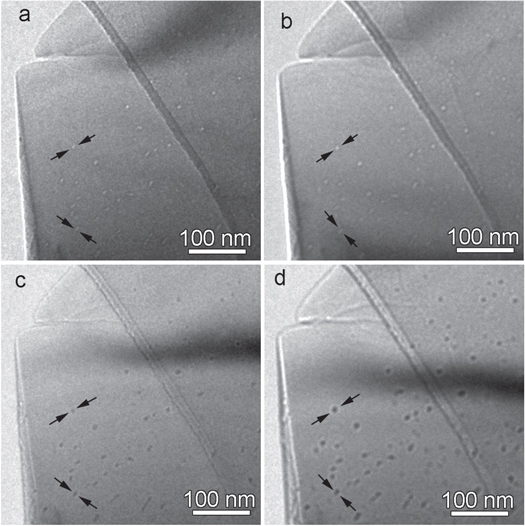
Figure 9. Through-focus series of TEM images from the same area inside a CaF2 grain containing ion tracks: (a) Δf1 < 0; (b) Δf2 < 0, ∣Δf1∣ < ∣Δf2∣; (c) Δf3 > 0; (d) Δf4 > 0, Δf4 > Δf3.
Download figure:
Standard image High-resolution image3.3. STEM–EELS results
During the previous TEM investigations performed in low e-beam conditions, we were able to discriminate the defects induced by SHI irradiation, ion tracks as rows of nanovoids, and those induced in situ, by e-beam irradiation during the TEM observation, undecidedly reported in literature either as voids or Ca colloids, or more generally, aggregated defects. By using STEM–EELS, here we provide evidence that the elemental composition within the ion tracks is indeed different from the surrounding matrix.
The STEM working mode is based on the mass-thickness contrast, meaning that signal intensity is proportional to the local 〈Z〉2 and the local sample thickness. On the other hand, EELS is an analytical technique providing qualitative and quantitative information regarding the chemical composition of the sample. By coupling STEM and EELS modes in the spectrum imaging (SI) mode, one can get data packages containing both morphological and spectroscopic information. In STEM–EELS–SI, the focused electron beam is scanned across the selected area while an EEL spectrum and morphologic information are acquired in each pixel. EEL spectra and composition maps can be afterwards extracted from the SI data cube with a space resolution which, in certain conditions, can go down to atomic resolution. We have applied the STEM–EELS analysis in order to get correlated chemical and morphological information on the irradiation defects induced by the heavy ions and the electron beam. The analysed grains contain both SHI and e-beam induced defects. The STEM images were acquired using the annular dark field (ADF) detector with a collection angle of 180–730 mrad.
On the STEM–ADF image in figure 10, the e-beam induced defects and the 23 MeV I ion tracks are indicated with white arrows and black arrow, respectively. For both kinds of defects, the characteristic contrast is darker than the surrounding area, indicating a local deficit of matter in both cases, which is in agreement with the conclusions derived from diffraction contrast of the underfocused/overfocused TEM images. The size of the observed defects, as measured on the STEM image, is in the range 2–4 nm for the irradiation track and about 10–15 nm or more for the e-beam induced defects (defect average size proportional to the time exposed to the e-beam), confirming the values resulted from the TEM study. Typical intensity line profiles across the ion tracks are presented correspondingly below the STEM images in figure 10.
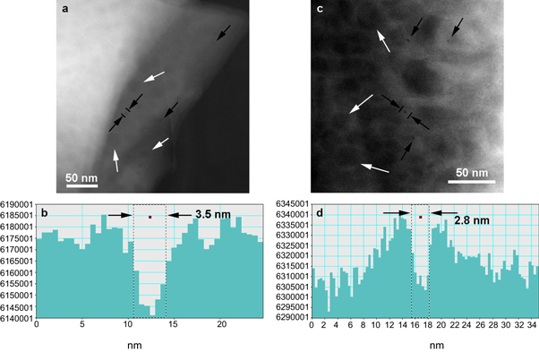
Figure 10. STEM ADF images (a),(c) at different magnifications (800 kx and 1200 kx) of a CaF2 grains containing irradiation tracks (black arrows) and e-beam induced defects (white arrows). Intensity line profiles across the irradiation tracks (b), (d) indicate their size (measured as the FWHM of the profile) in the range of 2–4 nm.
Download figure:
Standard image High-resolution imageThe possible chemical modifications associated with the irradiation-induced defects and the spatial distribution of the identified chemical elements were investigated by EELS in STEM mode (SI). On the STEM–ADF image in figure 11(a) (the same area as the one in figure 10(a)), the green rectangle marks a region containing one typical ion track (pointed by the black arrow) as well as defects created in situ by electron beam irradiation (pointed by white arrows). As previously mentioned, these defects show a darker contrast with respect to the surroundings, indicating a deficit of matter (void).

Figure 11. (a) STEM–ADF image of a CaF2 grain containing ion tracks and e-beam induced defects. The green rectangle indicates the area from which the Spectrum Image was acquired. (b) Elemental maps inside the green rectangle illustrating the local content of F and Ca; the composed RGB image was obtained by superposing the two elemental maps (c) EEL spectrum extracted from the entire area inside the green rectangle showing the absorption edges of Ca (L2,3 edge at 346 eV), F (K edge at 685 eV) and O (K edge at 532 eV).
Download figure:
Standard image High-resolution imageThe total EEL spectrum extracted from the whole SI area reveals the chemical elements Ca and F present in the sample. After removing the background, the local intensity of the Ca and F signals is mapped out as Ca and F elemental maps presented in figure 11(b). The two elemental maps were also overlapped into a composed coloured map to check for local chemical segregation. We have used the same arrows to point to the areas corresponding to the morphological details indicated in figure 10(a). Two interesting facts can be noticed by correlating the elemental maps with the STEM image:
- i.A local increase of the F signal and a deficit of the Ca signal correspond to the ion track.
- ii.A local deficit of the F signal and an increase of the Ca signal correspond to the e-beam induced defects.
On the composed coloured map one can clearly observe the spatial complementarities between the two elemental maps and the compositional differences between the ion tracks and the e-beam induced defects.
In addition to the expected Ca and F signals, the O absorption edge at 532 eV can also be noticed in the extracted EEL spectrum. The presence of the O signal is not surprising, since by TEM investigations we have evidenced the morphological and structural modifications of CaF2 under the e-beam and the in situ formation of cubic CaO during the TEM observation of the CaF2 grains (see the SAED patterns of the non-irradiated CaF2 single crystal grains after ca. 1 min of observation under focused beam, figure 1(e)).
3.4. RBS/c results
In agreement with the TEM results presented in section 3.1, RBS/c measurements provided evidence for damage build-up due to electronic excitation caused by the SHI irradiation. This was observed for all the SHI energies used, indicating again threshold below 2.9 keV nm−1.
For each CaF2 sample, the area irradiated by swift iodine ions was defined by a collimator 3 × 2 mm2 in size, and the channelling alignment was done on the unirradiated part of the sample. No sample preparation was done, and the ion current was kept low around 1 nA to obtain reliable RBS/c spectra. It was verified that the 2 MeV Li beam does not introduce defects after prolonged exposure, and that the RBS/c spectra from irradiated samples (containing disorder) can be reliably acquired even after multiple exposures. For each iodine energy used, three samples were irradiated with fluences of 3 × 1012 cm−2, 1 × 1013 cm−2 and 3 × 1013 cm−2, respectively. In total, nine samples were analysed by RBS/c. After the alignment procedure was accomplished on the unirradiated part of the sample, by a quick angular scan it was verified that the channelling axis is the same on the irradiated part of the sample. For each channelling RBS/c spectrum, a random one was also recorded for the same exposure time. In this way all aligned spectra could be normalised to the random spectra, ensuring all aligned spectra are normalised to the same analysing beam fluence.
In figure 12 we show RBS/c spectra for three different iodine energies, as a function of the applied fluence. It is evident that for each iodine energy used, disorder is introduced into the CaF2 crystal. Furthermore, by increasing the energy of the iodine ions, disorder is building up faster and eventually saturation is reached at the highest fluence. At that instance, obviously a second stage of damage evolves leading to a pronounced growth of the surface peak (marked by the arrow in figure 12).
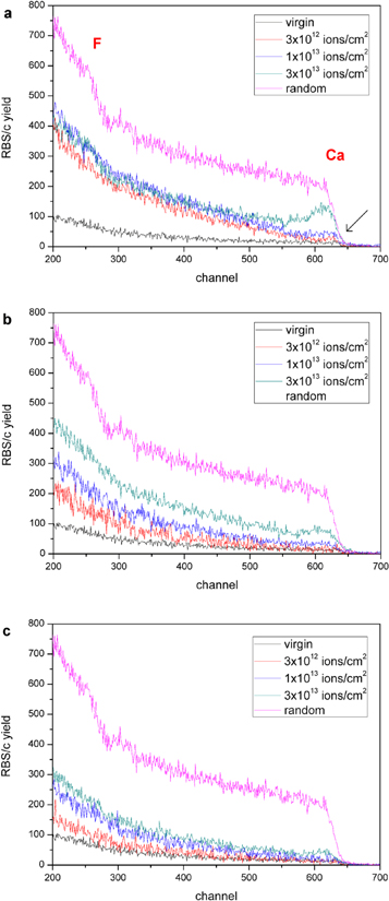
Figure 12. RBS/c spectra after (a) 23 MeV I (b) 15 MeV I and (c) 10 MeV I irradiation. The applied fluences were 3 × 10¹² ions cm−2, 1 × 10¹³ ions cm−2, and 3 × 10¹³ ions cm−2. For comparison, RBS/c spectra from unirradiated sample are given, both in channelling and in random orientation. Marked are Ca and F edges in the RBS/c spectrum and arrow points to the surface peak in (a).
Download figure:
Standard image High-resolution imageAnalysis of this kind of RBS/c spectra is usually done in the so-called surface approximation [27]. By neglecting the contribution from the surface peak, the amount of disorder Fd is measured by comparing the backscattering yield from defects (γi) relative to the backscattering yield in the random (γr) and aligned virgin (γv) RBS/c spectra at the position of the surface:

Assuming a cylindrical geometry for the ion tracks, it is possible to evaluate the radius of the individual ion tracks R by monitoring disorder build-up as a function of the applied ion fluence φ, and fitting the resulting data with a Poisson formula (thus taking into account ion track overlap):

where α is a normalisation factor.
It can be immediately realised this analysing approach is not adequate for the present set of experimental data. While it is clear that the damage is correlated to the electronic stopping power of the respective projectile, and the fact that ion tracks are observed by TEM for all used iodine ion energies, direct backscattering on defects below Ca edge (channels 300–650) is negligible. However, damage observed by RBS/c due to dechannelling of the probing beam in this region indicates damage within the F sublattice because direct backscattering of F atoms contributes to the RBS/c spectrum only below the F edge (i.e. below channel 300). In order to verify this, we have performed an additional RBS/c analysis using 1 MeV protons on the sample irradiated with 23 MeV I at a fluence of 3 × 10¹² ions cm−2. Due to different mass and energy of the probing ion beam, an enhanced sensitivity to backscattering from displaced fluorine atoms is achieved, as shown in figure 13. In this case, it is evident that both dechannelling and direct backscattering from the disordered fluorine lattice occur (increased RBS/c yield below channel 180) and in principle, the standard approach (i.e. surface approximation) could be applied to the fluorine edge in the RBS/c spectra. The pronounced step at the position of the fluorine surface indicates that most of the fluorine sublattice is disordered, in agreement with results from 2 MeV Li RBS/c (figure 12).
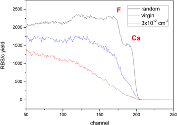
Figure 13. RBS/c spectra of samples irradiated with 23 MeV I ions at a fluence of 3 × 10¹² ions cm−2, obtained by 1 MeV proton probing beam. Marked are Ca and F edges in the RBS/c spectrum.
Download figure:
Standard image High-resolution imageSince dechannelling also depends on the defect concentration [51], dechannelling of 2 MeV Li below the Ca edge as a function of applied iodine fluence can be used for ion track measurement. Dechannelling here we define as the slope of the aligned RBS/c spectra between channels 400 and 600 in figure 12, corresponding to the depth of ca. 300 nm. Applying the Poisson formula (equation (2)) we estimate the ion track (i.e. disorder within fluorine sublattice) radii to be: R = 3.5 ± 0.1 nm for 23 MeV I, R = 1.6 ± 0.2 nm for 15 MeV I and R = 1 ± 0.2 nm for 10 MeV I irradiation (figure 14). For the 10 MeV I tracks, saturation of disorder below 1 cannot be ruled out (i.e. α < 1), but higher iodine fluences would be needed to establish this with certainty.
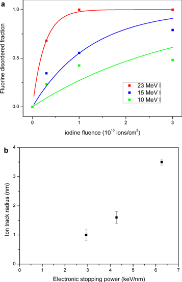
Figure 14. (a) Disordered fraction within the fluorine sublattice evaluated from the dechannelling RBS/c yield as a function of the applied iodine fluence for 23 MeV I (red), 15 MeV I (blue) and 10 MeV I (green) irradiation. (b) Ion track size increase with electronic stopping power.
Download figure:
Standard image High-resolution image3.5. AFM and ToF-ERDA results
While ion tracks were observed before on the CaF2 surface after grazing incidence SHI irradiation [52, 53], we demonstrate that for the creation of surface tracks a dE/dx of 2.9 keV nm−1 is already sufficient as can be clearly seen from the AFM images in figure 15. Surface ion tracks produced by grazing incidence 23 MeV iodine ion irradiation shown in figure 15(a) exhibit the typical, well defined nanohillock-like structure aligned along the SHI trajectory. This is in line with previously published data on surface ion tracks in CaF2 after grazing incidence with 103 MeV Pb ions [52]. The observed ion-track density at a fluence of 15 ion impacts μm–2 indicates a surface track formation efficiency close to one.
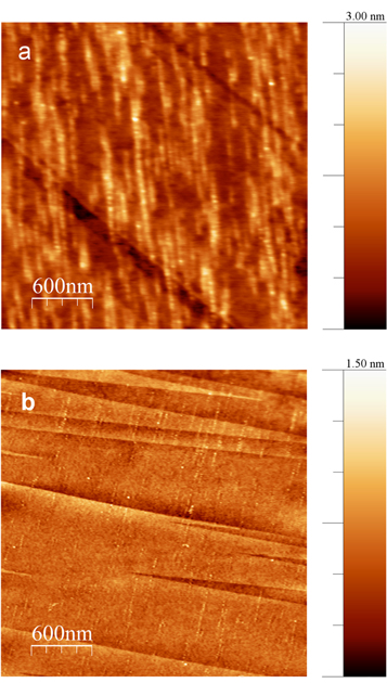
Figure 15. AFM images of the CaF2 (111) surface after irradiation with (a) 23 MeV I at 1° incidence angle and fluence of 15 ion impacts μm–2, (b) 10 MeV I at 1° incidence angle and fluence of 10 ion impacts μm–2.
Download figure:
Standard image High-resolution imageAfter 10 MeV I irradiation under the same grazing incidence angle of 1°, the resulting surface ion tracks show the same internal structure but they appear much fainter, as can be seen from figure 15(b). Images were acquired by the same AFM tip and on the same day, but we cannot rule out changes in the AFM tip quality during the measurements (figure 15(a) was acquired before figure 15(b)). However, the main point is that also here, the observed density of the surface tracks is in agreement with the applied fluence of 10 ion impacts μm–2 indicating that the track production efficiency is still close to one. Because one would expect a reduced efficiency close to the track formation threshold, we conclude that an electronic stopping power of 2.9 keV nm−1 (corresponding to 10 MeV I irradiation) is still well above the threshold for surface ion track formation. This is in agreement with the observation in [30], although thresholds for surface ion tracks produced in the normal and under the grazing geometry probably cannot be compared directly [19].
As shown previously, the formation of surface ion tracks after grazing incidence irradiation can be accompanied by depletion of one of the material constituents, resulting in non-stoichiometric surface state [19, 25]. For this reason, in situ TOF-ERDA was performed using 23 MeV I ions under the 1° grazing incidence geometry. As shown on figure 16, even after high fluence iodine irradiation (i.e. under the conditions of multiple ion tracks overlap), the stoichiometry of the CaF2 surface remains stable. This is not necessarily at variance with the STEM–EELS results presented in section 3.3. because information obtained from the ToF-ERDA is non-local since it inspects the whole sample surface.
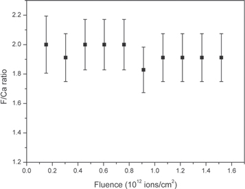
Figure 16. Calculated F/Ca ratio from offline analysis of the in situ ToF-ERDA measurements, obtained from the first 10 nm of the CaF2 sample. Measurements were performed using 23 MeV I ions at 1° grazing incidence angle.
Download figure:
Standard image High-resolution image4. Discussion
4.1. Discussion of TEM results
We begin by comparing TEM results obtained in this study with previously published data [32, 34, 35] and related analysis using the ITSM [27, 30] and the ATSM [26, 28, 31, 38]. The observation of surface as well as bulk ion tracks in CaF2 after irradiation with 10 MeV I, already at an electronic stopping power as low as 3 keV nm−1, is completely unexpected. From previous TEM studies, the threshold for ion track formation was evaluated to be at 9.5 keV nm−1 for low velocity irradiation [31, 32], while high velocity irradiation data indicated an even higher threshold around 20 keV nm−1 [34, 35]. Such a large value of the high velocity threshold, and the small size of the observed ion tracks was dismissed by Szenes as erroneous experimental data [28]. While it is true that TEM observation of ion tracks in CaF2 is challenging, due to the sensitivity of the material to e-beam irradiation as demonstrated in the present work, and due to known difficulties in evaluating the ion track diameter [33], objections of that kind cannot hold when clear experimental evidence for the existence of ion tracks is given. Here we note that the ion track sizes obtained in this study (data from section 3.1.) are comparable to other studies, with the exception of experiment with 40 MeV C60 cluster ion irradiation, as shown in figure 17. The slightly larger ion track diameter for the lowest energy irradiation (10 MeV I) is in our opinion not related to the nuclear stopping power. First, here presented RBS/c data show monotonic increase of disorder with increasing electronic stopping power. Second, 20.2 MeV Au4+ data point from a previous study [32], with nuclear and electronic stopping power of comparable magnitude, is indistinguishable from other irradiations with dominant electronic stopping power. Therefore, slightly larger ion track diameters cannot be caused by nuclear stopping power which is one order of magnitude lower than the electronic stopping power in all of our irradiations. Even if we assume that 100% of nuclear stopping power is transferred into the thermal spike, while only 20% of the electronic stopping power (a hypothesis that can be accommodated only within the ATSM), it would still not be possible to justify a track diameter of 5 nm after irradiation with 10 MeV I. At present we cannot explain this slight increase in ion track size after 10 MeV I irradiation, but as shown after in situ TEM measurements (section 3.2.) these measured ion track radii values are prone to uncertainties related to specific imaging conditions despite our efforts to keep imaging conditions similar for all the samples investigated. These measurements were done under low irradiation conditions, in order to limit or postpone the e-beam damage, and track sizes were estimated in the saturation conditions. Here we have to reiterate the warning of Szenes [28] because TEM results reported in previous works could also be influenced by the extreme sensitivity of the CaF2 to e-beam irradiation, as well as larger uncertainties due to a not so well defined geometry of the ion tracks [32, 33]. For that reason, we consider the RBS/c data (figure 14(b)) a better choice for thermal spike analysis than TEM data. Although RBS/c measurements also induce electronic excitations, the repeatability of the measurements indicate stability of the ion tracks during these measurements, probably due to much lower energies of the secondary electrons generated by the probing beam [54]. Therefore we conclude that by RBS/c pristine ion tracks can be observed, while during imaging by TEM ion tracks undergo certain development processes.
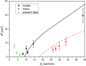
Figure 17. Track sizes in CaF2 observed by TEM. New data from the present study (only TEM data from section 3.1.) shown in green. Old data are taken from [32, 34, 35]. Lines are prediction of the ATSM according to [26].
Download figure:
Standard image High-resolution imageDespite the uncertainties with respect to the absolute size determination by TEM, our present study shows there can be no doubt that well-developed tracks form at stopping powers as low as 3 keV nm−1. Such a low value for ion track formation is not predicted by either one of the thermal spike models. To describe small ion track diameters in CaF2, ITSM invokes boiling as requirement for track formation observable by TEM, with a minimum deposited energy density of 1.7 eV at–1 [27]. Compared to the melting requirement for nanohillock formation with a minimum deposited energy density of 0.58 eV at–1 that is achieved at an electronic stopping power of 2.75 keV nm−1 for very low velocity ion irradiation [30], boiling (hence appearance of ion tracks observable by TEM) should not appear below an electronic stopping power of 8 keV nm−1.
The ATSM also faces difficulties in explaining the new experimental data presented here. Previously, the threshold of 9.5 keV nm−1 for ion track formation determined by TEM studies was attributed either to the absence of the velocity effect [31], i.e. the non-existence of a Coulomb explosion contribution at low velocities [24], or to the boiling mechanism like in the ITSM framework [26]. In both cases, ion tracks should appear along the ion trajectory at an electronic stopping power of 9.5 keV nm−1. Our observation, the appearance of tracks at 3 keV nm−1 is in clear contrast to these predictions. Even if we take into account that later on the predicted threshold was shifted down to 7 keV nm−1 (see figure 1 in [28]) a large discrepancy remains. Therefore, we can only conclude that the current descriptions of the ion track formation in CaF2 using thermal spike models are not entirely correct.
4.2. Discussion of RBS/c results
We now turn our attention to the RBS/c results. First, in agreement with the TEM data, disordering is observed already after 10 MeV I irradiation and increases with kinetic energy, hence it is an effect due to the electronic stopping power. Disordering is seen as an enhanced RBS/c yield due to dechannelling, while direct backscattering from disordered Ca atoms is observed only for the highest fluences, in the form of an enlarged surface peak. As shown exemplary for 1 MeV proton RBS/c (figure 13), this dechannelling originates from the disordered fluorine sublattice, and it should also represent the density of defects [51]. A similar approach was also used recently to assess SHI damage in diamond by simply integrating the RBS/c spectrum within the region of interest [55]. By applying the Poisson formula, we calculated from RBS/c spectra the ion track radii that corresponds to the extent of disorder within the fluorine sublattice after the ion impact (figure 14), indicating threshold at ∼2 keV nm−1. Qualitatively, the alleged anti-correlation with the TEM results is not completely unexpected. Close to the threshold, ion tracks observed by TEM are known to be bigger than tracks observed by RBS/c because of the discontinuous morphology of tracks having diameters below 2 nm [20]. Possible deviations from the Poisson formula would require accumulation of much more RBS/c data points that is out of the scope of the present work. Therefore, given the difficulties of the TEM analysis revealed in this paper, more than a qualitative agreement cannot be expected at present.
Next, we note that at least for the samples irradiated with 23 MeV I, the RBS/c spectra exhibit a saturation behaviour, in which case CaF2 is never fully disordered, in agreement with previous data [27]. This is an indication for a structural recovery of the Ca sublattice during high-fluence irradiation. At the moment it is not known if this is due to a so-called particle assisted prompt anneal (PAPA) mechanism [40] or a SHI beam induced epitaxial crystallisation (SHIBIEC) mechanism [56] operating on already existing ion tracks. The difference between the two mechanisms is that, in the first case, a recrystallisation would occur in the wake of the impacting ion (probably the mechanism responsible for the absence of ion tracks in crystalline Si [57]), while the second one considers the recrystallisation of defects produced by a previous ion impact. Regardless of the origin of this effect, the saturation in RBS/c spectra was also observed before in sapphire [58], reproduced here in figure 18. Actually, in the same work an enlargement of the aluminium surface peak was also observed, and it was stated that the damage kinetics is a two-step process. The driving force for the enlargement of the surface peak observed in sapphire is most likely due to the suppression of the recrystallisation process at the surface and at the crystal-amorphous interface [58–60].

Figure 18. RBS/c spectra for sapphire irradiated by 90 MeV Xe. Reproduced with permission from [58].
Download figure:
Standard image High-resolution image
It can be observed (figure 18) that up to the onset of the second step, i.e. up to the fluence of 4 × 10¹² ions cm−2, enhanced RBS/c yield from the aluminium step due to dechannelling increases with applied fluence. This can be attributed to disordering of the oxygen sublattice (that contributes only to dechannelling within the Al step), and indeed a monotonous increase of the oxygen edge due to backscattering of the RBS/c probing beam can be clearly seen. Saturation of the RBS/c yield observed for fluences of 3 × 10¹³ ions cm−2 and above coincides with a fully developed oxygen step, corresponding to a completely disordered oxygen sublattice. Apparently, the onset of the second stage of the damage evolution occurs when the oxygen lattice is fully disordered, but a more detailed analysis would be needed to verify this. Our results indicate that a similar two-stage process is active in CaF2. The reason why it was not observed in the previous study [27] is probably that it occurs only at high fluences, which are difficult to access by accelerators providing very high energy ions.
We note that for all of our RBS/c data points, disordering of the calcium lattice has not been observed (except for the surface peak enlargement at very high fluences during the second stage that we do not analyse here). Indeed, as shown in [27, 28], only for stopping power values above 7 keV nm−1, disordering of the calcium lattice can be seen. But we also note that for the 2 MeV He RBS/c spectrum of a CaF2 sample irradiated with low fluence high energy ions (375 MeV Pb, dE/dx = 29 keV nm−1 shown on figure 11(a) in [27], that dechannelling is substantial while direct backscattering of ions from the Ca lattice is minimal. Only for higher fluences can backscattering from disordered Ca atoms be observed due to disordering of the Ca sublattice. Therefore, we conclude that two separate values of the ion tracks (and corresponding thresholds) can be extracted from the analysis of RBS/c data: one that is related to disordering of the fluorine sublattice and another one that is related to disordering of the calcium sublattice. In our opinion, both values are relevant for the present and previous RBS/c analyses of ion tracks in CaF2 and both cannot be described with a single set of model parameters, unless one invokes different track formation criteria. Perhaps other techniques, like for example optical absorption spectroscopy, can provide more insight into these defects because the observed formation of coloured centres was identified to be due to the electronic excitations [61], even below 5 keV nm−1 [37].
4.3. Elemental composition of ion tracks in CaF2
Finally, we turn our attention to the question of the composition of the individual ion tracks in CaF2. Based on previous observations of electron induced defects in CaF2 [39], anion nanovoids were assumed to be the building blocks of intermittent ion tracks in CaF2 observed by TEM [32–35]. Still, the whereabouts of the fluorine remained an open question. Presumably released as a gas, it was proposed that it is efficiently released from within the ion track [35]. Alternatively, it was proposed by Chadderton [40] that fluorine can remain trapped within the material but outside the ion track.
Our results provide some new insight on this topic. By corroborating the morphological and spectroscopic information resulting from the diffraction contrast images in TEM, mass-thickness contrast images in STEM, STEM–EELS elemental maps we come to the following conclusions:
- i.The observed ion irradiation tracks consist of rows of nano-voids (lower Ca signal in the EELS elemental maps) where F may be trapped in gaseous state (higher F signal in the EELS elemental maps).
- ii.The e-beam induced defects consist in nanometric volumes where CaF2 dissociates with the likely loss of gaseous F2 and formation of Ca-rich nanometric pockets where Ca is partially oxidised (due to the residual oxygen atoms in the TEM column vacuum). As mentioned also in [33], the mass density of Ca (1.54 g cm−3 is lower than the one of CaF2 (3.18 g cm−3, which explains the void-like behaviour of the diffraction contrast in the TEM images of the e-beam induced defects. The remaining Ca-rich regions are partially oxidised as proved by the SAED patterns and EEL spectra.
In addition, we have shown that by irradiating CaF2 at grazing incidence angle using a 23 MeV I beam, well developed ion tracks can form, as seen by AFM. In situ ToF-ERDA measurements using the same ion beam parameters, provide evidence that the surface composition does not change. This evidence rules out the fluorine gas release scenario, and STEM–EELS provides further support that fluorine remains trapped within the ion track. However, the loss of calcium as seen by STEM–EELS is surprising, and apparently at odds with ToF-ERDA results. But, these results are not necessarily mutually inconsistent, because ToF-ERDA provides information on the macroscopic scale, and STEM EELS on the microscopic one. Furthermore, as mentioned in section 4.1, secondary electrons generated by SHIs (in this case also ToF-ERDA beam) have much lower kinetic energies [54] than e-beam used for STEM EELS, and therefore less damaging to the CaF2 structure. In that sense, STEM EELS results provide further insight about the development of the ion tracks during the TEM measurements (section 3.2).
We propose the following interpretation of our results. Although many of the CaF2 chemical bonds are broken by SHI irradiation, Ca ions remain in place probably due to recrystallisation of the Ca sublattice (inferred from RBS/c data [27]), while F ions are disordered, as indicated by the RBS/c results reported in the present work. The RBS/c probing beam seems to leave the ion track structure unaffected, but in the TEM the ion tracks evolve continuously under the e-beam via radiolysis processes. At the beginning of the TEM observation, no contrast of ion tracks is visible, and this should correspond to the situation that we find by RBS/c measurements, with disordered F and non-disordered Ca sub-lattices. Only after a few tens of seconds, ion tracks are revealed in the TEM because the broken Ca–F chemical bonds are not restored by the e-beam in the microscope. On the contrary, Ca partially diffuses inside the neighbouring CaF2 lattice, and the ion track becomes enriched in F, as indicated by EELS–SI. The Ca out-diffusion from the ion tracks into the surrounding lattice corresponds to the ion track developing process observed by in situ TEM. The resulting ion track consists then of a channel formed with a lower density of Ca atoms, i.e. enriched in fluorine, which explains the contrast observed by defocus in conventional TEM observation. Recent results on e-beam irradiated CaF2 that indicate a loss of calcium for high enough electron fluences provide further support for such scenario [50].
5. Conclusion
By using RBS/c and TEM techniques, we present evidence of ion track formation in CaF2 for electronic stopping power values as low as 3 keV nm−1, which suggests melting as requirement for ion track formation. We also present a new way of analysing RBS/c data giving clear indications for disordering of the fluorine sublattice at these low stopping powers, even under conditions when the calcium sublattice remains undamaged, probably due to recrystallisation. Bulk ion tracks observed by TEM after SHI irradiation at low stopping powers used in this study, indicate that current interpretations of ion track formation in CaF2 using the thermal spike mechanism (either related to boiling within the ITSM or absence of Coulomb explosion contribution within the ATSM) are likely inadequate. Alternative explanations such as the PAPA [40], SHIBIEC [56] or exciton related mechanisms [6, 62] should be checked in future experimental studies.
The relationship between previously published RBS/c data [27] and data presented here remains unaddressed, since the former should be re-evaluated using the method demonstrated here. The TEM data presented here shows convincingly that the evaluation of ion track sizes using this technique results in ambiguous results, depending on the imaging conditions. To what extent previous data are subject to these effects remains unknown to us, but we believe our findings provide support to Szenes questioning of TEM data in that respect.
Surface ion tracks were also produced after grazing incidence SHI irradiation for the same low value of electronic stopping power, showing the well-known intermittent structure. Both ToF-ERDA and STEM–EELS experiments provided evidence that fluorine remains within the material when ion tracks are formed in CaF2.
Acknowledgments
MK, ZS, MJ and SF acknowledge the financial support from the Croatian Science Foundation (pr. No. 8127). Support from the Croatian Centre of Excellence for Advanced Materials and Sensors is also acknowledged. CG and RFN acknowledge the financial support from Core Project PN16-480102. CERIC-ERIC consortium is also acknowledged for the support.