


Abstract
Determining the scattering potential landscape for two-dimensional superlattices provides key insight into fundamental quantum electron phenomena. Theoretical and semiempirical methods have been extensively used to simulate confinement effects of the two-dimensional electron gas (2DEG) on superlattices with a single scatterer in the form of vicinal surfaces and dislocation networks or isolated structures such as quantum corrals and vacancy islands. However, the complexity of the problem increases when the building blocks (or scatterers) are heterogeneous, as in metal-organic nanoporous networks (MONNs), since additional potentials may come into play. Therefore, the parametrization of the surface potential landscape is often inaccurate, leading to incorrect scattering potentials. Here, we address this issue with a combination of scanning tunneling microscopy/spectroscopy, angle resolved photoemission spectroscopy and Kelvin probe force microscopy measurements together with electron plane-wave expansion simulations on a MONN grown on Cu(111). This experimental-theory approach, enables us to capture the 2DEG response to the intricate scattering potential landscape, and reveals systematic modeling procedures. Starting from a realistic geometry of the system, we determine the repulsive scattering potentials for both molecules and coordinated metal adatoms, the latter contradicting the established simulation framework. Moreover, we reveal local asymmetries and subtle renormalization effects of the 2DEG that relate to the interaction of the MONN and the underlying substrate.
Export citation and abstract BibTeX RIS

Original content from this work may be used under the terms of the Creative Commons Attribution 3.0 licence. Any further distribution of this work must maintain attribution to the author(s) and the title of the work, journal citation and DOI.
1. Introduction
Shockley states on (111)-terminated noble metal surfaces provide textbook examples of a 2DEG [1], presenting adequate model systems to study electron confinement effects. These surface states (SS) exhibiting no overlap with the bulk states emerge from the atoms of the outermost surface layers and are therefore very sensitive to surface impurities [2, 3], to structural defects in the form of atomic steps or vacancy islands [4–9] and to thin overlayers comprised by e.g. rare gases and alkali metals [10]. Indeed, the electrons from the 2DEG can be confined by enclosed structures such as mechanically assembled quantum corrals [11] and nanometer sized vacancy islands [6, 12] and their electronic properties could be determined from simple particle in a box models [13] and numerical approaches [6, 12]. In well-defined stepped arrays, for instance, the physical nature of the modulated electronic bands can also be captured by applying the 1D-Kronig Penny model [14]. In this model, the steps are considered repulsive, square-shaped finite potential barriers of magnitude U0 × b, where U0 corresponds to the height of the barrier and b to its width [15]. Likewise, molecular adsorbates scatter the SS by their repulsive potential backbone [16], producing 2D confinement effects in concave [17] or closed structural arrays [18, 19]. In the case of nanoporous molecular networks, each pore defines a single quantum dot (QD) that coherently couples with identical neighboring confined states. When the arrays are periodic and long-ranged, they generate characteristic shallow dispersive bands [20, 21]. These surface specific electronic bands originating from the pristine Shockley state [22] can be delicately tuned by increasing the QD barrier separation (thus reducing the interpore coupling) [23], pore size [19] and also by changing the pore shape [24].
The modelization of electron scattering by 2D arrays (organic and metal-organic nanoporous networks) is often performed using the electron boundary element method (EBEM, for finite systems) or the electron plane wave expansion (EPWE, for infinite periodic systems). While the former approach only accounts for the local confinement response (local density of states), the latter also captures the electronic band structures arising from Bloch-wave states and generated from interdot coupling [18, 19, 23, 25–28]. However, it is a semiempirical method, and therefore some assumptions are required regarding the potential barrier strength, corresponding sign (repulsive/attractive) and geometries, which often lead to arbitrary or unphysical conditions. In particular, unrealistically thin molecular backbones have been employed, leading to modified effective pore sizes [18, 19, 27]. In addition, attractive scattering potential regions at the metal sites in 2D MONNs [18, 19, 25] or enlarged effective masses (m*) compared to the 2DEG reference [23, 25] have been assumed. This raises the question whether such (to some extent arbitrary) assumptions are necessary when simulating the electron confinement by these MONNs. Here, we address this question by studying in detail the interaction between the 3deh-DPDI network [20, 22, 25, 29–33] and the Cu(111) 2DEG. Based on a combination of scanning tunneling microscopy and spectroscopy (STM and STS), angle-resolved photoemission (ARPES) and Kelvin probe force microscopy (KPFM) measurements, together with EPWE simulations, we demonstrate that both local confinement effects and the emergence of electronic bands induced by interpore coupling can be satisfactorily reproduced. This is achieved by starting from a realistic scattering geometry and then assigning physically meaningful scattering potentials to its barriers (both for molecules and adatoms). We shall show that to this end, we require a 2DEG renormalization that affects both the effective mass (m*) and energy reference (ERef). Our explanation for these changes is based on the alteration of the vacuum region upon network presence, which is known to partly define the Shockley state [34, 35]. This combination of experiment and theory enables us to capture the intricacies of the scattering potential landscape, and to establish systematic modeling procedures.
2. Results
The organometallic network that we study is formed by deposition of the organic dye DPDI (4,9-diaminoperylene quinone-3,10-diimine), which undergoes a dehydrogenation process when deposited on Cu(111) and heated to 250 °C. The resulting organic building block 3deh-DPDI is an 'exo-ligand' coordinated to Cu adatoms that forms a long-range ordered, commensurate MONN [20, 22, 29–33, 36]. The unit cell is composed of 3 molecules and 6 Cu adatoms. The network bears a periodicity of 25.5 Å and is three-fold symmetric. The three-fold symmetry of this network arises from the different registry of the coordinating Cu adatoms with the surface: one type of Cu trimer (i) is centered on an 'on top' site, while the other Cu trimer (ii) surrounds a hollow site [30, 33].
Figure 1 shows this network and compares the experimental STM/STS data (center row) with two EPWE simulations obtained using the scattering geometry shown in panels (a) and (g) and barrier potentials specified in table 1. The top row in figure 1 assumes the scattering geometry proposed in [25], which is formed by hexagons at the Cu adatom coordination sites (in green) connected by molecular potentials of 5.5 Å width (in purple). In this model the metal adatom regions dominate spatially over the molecules and the simulated potential landscape weakly resembles the STM topography of figure 1(d) and the structural model of the MONN in particular (see figure S1 is available online at stacks.iop.org/NJP/21/053004/mmedia). Furthermore, the potential at the Cu coordination region presents a negative sign, denoting attractive scattering character to this region, similar to other simulated MONNs [18, 19]. Using the 2DEG reference of ERef = −440 meV (at 5 K) and  (slightly larger than for the pristine substrate), we find in the simulations a very good match for the n = 1 partially localized state (n = 1 PLS) to the experimentally obtained dI/dV map. However, this good agreement is lost for the higher orders (vertically compare figures 1(b) and (e)). Note, for instance, that the LDOS central intensity is reversed for the highest energy dI/dV map shown. Similarly, when comparing the dI/dV spectra at selected unit cell positions (figures 1(c), (f)), we find that only the pore center spectrum (PC, in red) acceptably matches the experimental one, but the rest deviate strongly as the bias exceeds −0.12 V. Firstly, at the halfway spectrum (H, in blue), the dominant peak at +0.32 V is experimentally absent. Secondly, for the metal center (Cu, in green), two prominent peaks are observed at −0.09 V and +0.18 V and show a drop of the intensity at the right side of the simulation, which are not found in the experimental data. In particular, the strong localization at the Cu atoms for the +0.18 V state, with LDOS as large as the fundamental n = 1 PLS, markedly deviates from the experiment, indicating unphysical potential assignment at this position.

Figure 1. EPWE simulated and experimental LDOS data obtained for the 3deh-DPDI MONN on Cu(111). The top (a)–(c) and bottom (g)–(i) rows correspond to two different EPWE parametrized simulations that we compare to the experimental case shown at the center row (d)–(f). The central row consists of a topographic STM image (d), three dI/dV maps at constant height at different energies (−0.186 eV (n = 1 PLS), 0.016 eV (n = 2 PLS) and 0.385 eV (n = 4 PLS)) (e) and four dI/dV spectra acquired at different positions of the unit cell (see inset) (f). All experimental data can be vertically compared to two EPWE models: the top row reproduces the one in [25] and the bottom one is proposed in this work. The scattering geometries shown in (a) and (g) consist of three parts: Cu substrate area (shown in red), molecules (purple rectangles) and metal coordination regions (green hexagons). The corresponding potential values are indicated in table 1. Experimental parameters: tunneling parameters in (d) are −200 mV/700 pA; dI/dV maps (e) and dI/dV spectra (f) obtained from grid spectroscopy measurement (35 × 30 points) with initial tip conditions of 400 mV/70 pA and lock-in frequency 513 Hz; zero-to-peak amplitude: 8 mV. A binning of 30 meV is applied to each dI/dV map.
Download figure:
Standard image High-resolution imageTable 1. EPWE potential parameters used in the models discussed throughout this work. Vmol refers to space occupied by the molecule and Vmet to the metal coordination centers, which are respectively shown as purple rectangles, and as green hexagons in figures 1(a) and (g). The large red areas corresponding to the Cu substrate are fixed to Vsubs = 0 eV. The 2DEG scattering reference (ERef at 5 K) and m* used for the EPWE simulations is indicated in the two rightmost columns. The first model is taken from [25], the second one is generated from a realistic geometry of the network, whereas the third one is identical to the second model, but differentiates the two types of metal coordination centers and discussed in detail in figure 2.
| Vmol (meV) | Vmet (meV) | ERef (meV) |

|
|
|---|---|---|---|---|
| Model 1 [25] | 1500 | −100 | −440 | 0.44 |
| Model 2 | 390 | 390 | −440 | 0.49 |
| Model 3 | 390 | 440 (green) | −440 | 0.49 |
| 340 (purple) |
The pronounced discrepancies between the experimental data and the EPWE model generated with the parameters of [25] (Model 1) led us to reconsider the scattering geometry and potentials in these simulations. Based on the structural model of the MONN proposed in earlier work [30, 33] (see figure S1), we start from a more realistic geometry where the molecular backbones dominate, instead of the metal coordination regions (see figure 1(g)). This leads to a more accurate molecular geometry of 9 Å in length and 8 Å in width and much smaller metal coordination regions that fill the space left between the molecules. Instead of allowing this geometry to change, we provide flexibility to the 2DEG reference [23, 37]. We find that using ERef = −440 meV (for 5 K) and  , the latter notably deviating from the pristine Cu(111) SS [4, 38], together with homogeneous repulsive barriers both for molecules and metal centers (
 ), we can capture most details of the experimental LDOS and dI/dV spectra. We would like to point out that these values were not arbitrarily chosen (scattering parameters indicated as Model 2 in table 1), but are the result of simulating the combined ARPES and STS experimental data [23, 37]. These parameters turn out to be crucial for moving the higher order confined states to lower energies (for instance lowering n = 4 PLS to ∼0.49 V) (see figures 1(h) and S3). Interestingly, the dI/dV spectrum on top of the metal adatom region (green curve) shows a relevant attenuation of the spectral features above −0.1 V that agrees very well with the experimental curves and corroborates the repulsive character of this region of the network (figures 1(f), (i)).
We provide further support for the choice of repulsive scattering parameters for both molecules and metal centers by performing local contact potential difference (LCPD) measurements using the KPFM method [39, 40]. The KPFM contrast is known to qualitatively relate to the z-component of the electrostatic field Ez at a constant-height plane above the molecule. The simple interpretation is that a more positive LCPD corresponds to more negative charge below the tip. Even though the tip radius is expected to be much larger than the local variations of the surface potential, in figure 2(a), we observe that the molecular scattering backbone (in red) is similar in size to the molecular dimensions. In addition, the smaller Cu coordination regions, which appear less intense than the molecules (most probably due to their different height [30]), do not drastically change their color when compared to the pore regions, ruling out any tendency towards a sign reversal of the scattering potential and therefore maintaining a repulsive character for the surface electrons.
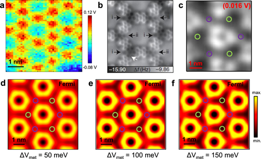
Figure 2. Corroboration of three-fold symmetry at metal coordination positions, influence upon the confined states and EPWE implementation. (a) Kelvin probe force microscopy image of several pores showing LCPD variations at the sub nanometer scale confirming the existence of surface potential variations upon the formation of the molecular network. (b) Noncontact AFM measurements (adapted from [33]) with sub-molecular resolution differentiating the two types of metal coordination centers (denoted i and ii). (c) dI/dV constant height map for the n = 2 PLS (slightly above EF) indicating the different metal adatom regions as two colored circles (purple and green). The sensitivity to the threefold symmetric potential is demonstrated by the triangular shape (instead of hexagonal) observed inside the pore. The LDOS asymmetry can be simulated in EPWE as a perturbation of the scattering potential. In particular, (d)–(f) shows a sequential perturbation of the hexagonal n = 2 PLS (Model 2), when potential variations of ΔVmet = 50 meV, ΔVmet = 100 meV and ΔVmet = 150 meV are considered respectively. The green metal coordination position has a higher potential value than the purple one and, correspondingly, the distortion becomes stronger the larger this difference is. The LDOS shown were calculated at the Fermi energy.
Download figure:
Standard image High-resolution imageThe LDOS simulation shown in figure 1(h) displays a six-fold symmetry that contradicts previous experimental findings reporting the existence of two structurally different adatom coordination sites within the network [30, 33]. This difference is explained as a variation of the registry with the substrate, where the geometric center of the three metal adatoms either lies above a three-fold hollow site or a Cu atom of the substrate. This subtle variation shows up in the AFM images acquired with a CO functionalized tip (see figure 2(b)) and in the dI/dV maps whenever the intensity shifts away from the pore center, as is the case of n = 2 PLS (see figure 2(c)). It is worthy to note that this is the first experimental observation of the triangular shape of n = 2 PLS, although they were predicted for hexagonal lattices with three-fold symmetry [24]. EPWE can simulate this behavior by inducing a slight potential variation (ΔVmet) between Cu regions while keeping the molecular potential at Vmol = 0.39 eV (Model 3 in table 1). In this way, we observe a clear transition of the n = 2 PLS from hexagonal to triangular, as shown in the bottom row of figures 2(d)–(f). We find that the green regions correspond to a stronger potential than the purple regions, which are likely related to subtle differences in vertical packing. Based on the ∼25 meV potential difference between fcc and hcp sites of the Au(111) surface [41], we tentatively assign the green sites to larger potentials (fcc) and the purple to lower ones (hcp). Such potential variation induced effects are experimentally discernible in the dI/dV spectra when comparing the two different Cu-coordinated sites, which can be reproduced following Model 3 (see figure S4). Note that this symmetry reduction of our MONN considerably affects n = 2 PLS, but leaves the higher n = 4 PLS almost unperturbed (see figure S5).
The synergy between our local spectroscopies and EPWE simulations has produced two relevant results: first, the metal coordination sites exhibit repulsive scattering potential character, which is required for the presence of three-fold symmetry in the higher energy states and, second, a mass renormalization of the 2DEG that occurs upon the presence of the network on the Cu(111) surface. These findings should be compatible with the ARPES data shown in figure 3. This dataset corresponds to the situation in which the 3deh-DPDI network completely covers the surface and no trace of the Cu SS is observed (figure S1). It is straightforward to confirm that the 2DEG renormalization is correct since both the simulated band structure and the isoenergetic cuts fit well the experimental data when using the scattering parameters indicated in Model 2 of table 1. In figure 3(a), the second derivative of the experimental data (raw data in figure S2) exhibits the expected shallow dispersive bands of QD arrays [20, 22, 23, 27]. The lower energy band corresponding to n = 1 PLS has a ∼80 meV bandwidth and shifts ∼150 meV towards EF with respect to the pristine Cu SS and increases m* to  [20, 23, 32]. This effective mass is higher than the 2DEG reference as a result of the confinement induced by the nanoporous network [23, 37], which is certainly substantial judging from the prominent energy gap (120± 30 meV) detected at the zone boundaries (
 point) separating the n = 1 and n = 2 PLS bands [42]. Note that the effective mass of
  results from the fit of a parabola to the experimental data close to the
  point, assuming a free-electron-gas. However, the assumption of a free-electron-gas may not be the most appropriate model for describing the pertaining shallow dispervise n = 1 PLS band generated by coupled confined states. Thus, the extracted effective mass value considerably differs from the
  used in EPWE Model 2, but supports the 2DEG mass renormalization.

Figure 3. Experimental and simulated electronic band structures and isoenergetic maps of the 3deh-DPDI network completely covering the Cu(111) surface. (a) Energy dispersion maps for the two high symmetry directions  and
and  . The color plot represents the second derivative of the intensity to enhance the weak details with respect to energy and parallel momentum. The high quality of the network allows to observe faint replica bands in adjoining Brillouin zones. Simulated EPWE bands using the scattering potentials of Model 2 (see table 1) are superimposed as red lines onto the experimental data and perfectly match both high symmetry directions. Experimental (b) and simulated (c) isoenergetic cuts (kx versus ky) in second derivative obtained at the band-bottom (−0.24 eV), lower edge of the
  point (−0.13 eV), inside the gap (−0.07 eV) and at the Fermi level. As a reference, the MONN induced hexagonal surface Brillouin zones are superimposed onto the second derivative data. Experimental ARPES parameters:
  , Ts = 10 K for (a) and Ts = 150 K for (b).
Download figure:
Standard image High-resolution imageThe three-fold symmetry observed in the LDOS for the n = 2 PLS is absent in the Fermi surface map of figure 3(b). Instead, all isoenergetic cuts (kx versus ky) exhibit six-fold symmetry (hexagonal shape) that diverges from the circular and isotropic pristine Cu SS. It could be argued that due to the averaging character of ARPES, the illuminated (probed) area contains, with equal probability, network patches with (i) and (ii) metal coordination regions at equivalent pore sites (60° relative rotations). Nonetheless, the fundamental reason for the observed higher symmetry is the conservation of time reversal symmetry, which requires E(k) = E(−k). Hence, isoenergetic cuts should appear as six-fold even if a single three-fold symmetric 3deh-DPDI network domain was present on the surface. This is in agreement with other three-fold symmetric surface structures such as Ag/Cu(111) superlattices, where the band structure also appears as six-fold symmetric [43]. Indeed, using the scattering parameters of both Models 2 and 3 in table 1, the electronic band structure agrees with the band structure dispersion, gap size and isoenergetic shapes experimentally observed (figures 3(a)–(c)). This very satisfactory agreement between theory and experiment supports and validates the repulsive scattering character assigned for molecules and metals, as well as the imposed renormalziation of the 2DEG reference.
3. Discussion
Our results demonstrate that an appropriate EPWE simulation of the electron confinement by QD arrays should be achieved by having at hand STM/STS and ARPES experimental data and using realistic geometries of the overlayer before defining the strength of the scattering potential barriers. Moreover, the 2DEG reference requires certain flexibility, especially in m*, in agreement to previous work [23, 25, 37]. The 2DEG reference changes upon presence of the organic overlayer, as schematically shown in figure 4(a). The resulting (leaky) confinement depends on the detailed potential landscape imposed upon the 2DEG by the nanopouros network, defining the interpore coupling and producing new electronic bands separated by gaps at zone boundaries [23, 27].

Figure 4. Reported renormalization of 2DEGs by physisorbed overlayers. (a) Schematic band renormalization of the Cu Shockley state resulting in an increase of its reference energy and effective mass upon the presence of the studied nanoporous network. (b) Renormalization chart (ΔEB versus Δm*) reported for families of physisorbed systems onto substrates exhibiting 2DEGs. Nanoporous networks (yellow area) [23, 32, 37] are compared with rare gas overlayers (orange area) [44, 45] and with graphene [46, 47] and h-BN [48] (blue area). Note that m* renormalization becomes relevant only for nanoporous networks.
Download figure:
Standard image High-resolution image
The proposed 2DEG renormalization is not uncommon and has been observed in numerous physisorbed overlayers, such as graphene (Gr), boron-nitride (hBN) and rare gases physisorbed on noble metals. Figure 4(b) compiles selected results from these related systems where the SSs shift towards the Fermi level while varying their m*. It is interesting that even if the energy shifts can be of similar magnitude, the effective masses do considerably increase in the case of nanoporous systems. This is likely caused by the QD coupling extending through the surface.
Once the 2DEG reference modification has been justified, the scattering potential values call for attention. When comparing the molecular potential Vmol obtained in this work (see table 2) we find that its value (390 meV) is larger than other reported cases with experimental ARPES data [23, 37]. The 3deh-DPDI MONN features potential barriers capable of strongly confining the surface electrons and opening significant energy gaps in the band structure. Nevertheless, the magnitude of the value is reasonable when compared to other networks, suggesting that limitations to the potential magnitude should exist when used to simulate the molecular scattering potentials. As an educated guess, this limit could be of the order of  . Note, however, that ultimately the effective potential that 2DEG electrons encounter depends on the separation between pores, i.e. the molecular widths. The proposed upper boundary value would also be restricted to planar and single layer molecular systems.
Table 2. Scattering potential values for molecules (Vmol) and metal centers (Vmet) for three different types of organic and MONNs. The selected networks correspond to the one from this study (top row), the homothetic Co-coordinated para-hexaphenyl-dicarbonitrile (Ph6Co) and para-terphenyl-dicarbonitrile (Ph3Co) MONNs on Au(111) (middle) and two halogen bonded Br-DNT and Br-DNF networks on Ag(111) (bottom row). The values are taken from EPWE simulations based on STS and ARPES datasets.
| Vmol (meV) | Vmet (meV) | |
|---|---|---|
| 3deh-DPDI network | 390 | 340 / 440 |
| Ph6Co / Ph3Co [37] | 250 | 50 |
| Br-DNT / Br-DNF [23] | 140 | — |
Furthermore, we demonstrate that the scattering character of the adatom metal centers is repulsive for the 3deh-DPDI network. This follows a similar pattern to molecular backbones and to other atomic-like surface 2DEG confining entities in the form of step edge adatoms, quantum-corral barriers or dislocation networks [11, 14, 49]. We infer that this effect is quite general and has in the past been incorrectly considered for the case of organometallic nanoporous networks [18, 19, 25]. Indeed, the repulsive values proposed for Ph6Co and Ph3Co in table 2 [37] are more physically sound and in agreement with the present observations.
It is interesting to discuss further the implications of the observed LDOS deviation from the hexagonal shape induced by scattering potential imbalance at the metal sites. The local three-fold appearance of the higher order n = 2 PLS comes not solely as variations of the metal center registry with the substrate (as shown here in figure 2), but can also be generated from small relative displacements of the building blocks defining the pores. An example of the latter has been already reported for chiral networks stabilized by hydrogen bonds [24]. Accordingly, it is the ultimate geometry of the tectons that dictates the LDOS shape if the scattering potential barriers have similar magnitudes.
Finally, it is plausible that the confined pore states could play a role in guest filling of QD arrays by increasing the adsorption energy [24, 50]. A way of confirming this hypothesis would require the observation of certain symmetries imposed on the guest species adsorbed into the QDs. In particular, the 3deh-DPDI nanopores can host up to 12 Xe atoms per pore that are clustered into four atom bunches [31]. Since these rare gas atoms maintain exactly the same relative bunch orientation for all neighboring pores in an overall three-fold symmetry, we infer that the n = 2 PLS (closest to the EF) can participate in guiding the observed Xe pore condensation. Alternatively, these Xe atoms could be just marking three equivalent metal sites exhibiting the lowest surface potential of the whole network [51].
4. Conclusions
In conclusion, we have shown that it is possible to obtain the scattering potential landscape exerted by a nanoporous metal-organic overlayer onto a 2DEG and determine the relevant confinement details and interaction effects. This is achieved by combining semiempirical EPWE simulations with local and averaging electronic experimental techniques (STM/STS, AFM, KPFM and ARPES). We showed that the scattering potential must be parametrized as realistically as possible to the network geometry while providing flexibility to the 2DEG, which requires a slight energy/mass renormalization due to the interactions between overlayer and substrate. Our simulations unambiguously establish that both the molecules and the metal adatoms forming the network exhibit repulsive interactions with the surface electrons. We provide a tentative upper limit to the magnitude of such repulsive scattering of the network components for related MONN systems. We also find that slight perturbations in the scattering potential at the metal sites are responsible for the deformation of the confined states, which display three-fold symmetry. Our work confirms that the confined 2DEG is sensitive to existing subtle interactions of the overlayer with the substrate and corroborates the SS renormalization, which provides consistency to the results obtained by these semiempirical simulations.
Acknowledgments
We acknowledge the financial support from the Spanish Ministry of Economy, Industry and Competitiveness (MINECO, Grant No. MAT2016-78293-C6), from the Basque Government (Grant No. IT-1255-19), from the regional Government of Aragon (RASMIA project). Part of this work has been performed at the SOLEIL synchrotron at the CASSIOPEE beamline under proposal 20080787. We acknowledge support by the Deutsche Forschungsgemeinschaft (SFB 1249, TP A2 to LHG). SK acknowledges support by Japan Society for the Promotion of Science (JSPS) KAKENHI Grant Number 15K21765. We also acknowledge funding by the Paul Scherrer Institute, the Physics Department of the University of Basel and the Swiss Nanoscience Institute, the Swiss National Science Foundation (Grants # 200020_162512, 206021_144991, 206021_121461) and the Swiss Commission for Technology and Innovation (CTI, 16 465.1 PFNM-NM).