


Abstract
We report on the electronic and optical properties of ultrathin granular films. We demonstrate that the static dielectric constant increases with thickness in the dielectric regime and diverges at the critical thickness, as predicted by classical percolation theory. However, for thicker samples, the dc conductivity does not obey scaling laws due to the presence of tunneling conduction. In this region the dielectric constant is positive, and the electronic transport is not metallic but can be described by Jonscher's universal power law, even though there is a Drude-like response indicating the presence of free charge carriers. Only for thicker films when the dielectric constant becomes negative is there metallic conduction.
Export citation and abstract BibTeX RIS

Original content from this work may be used under the terms of the Creative Commons Attribution 4.0 licence. Any further distribution of this work must maintain attribution to the author(s) and the title of the work, journal citation and DOI.
Granular metals consisting of metal nanoparticles randomly distributed in an insulating matrix have received particular interest in the research field of modern condensed matter physics due to their fascinating electrical, magnetic and optical properties [1–7]. For example, granular metals have attracted significant interest as engineered plasmonic metamaterials [8, 9], and for photocatalysis [10] and microwave applications [11]. On the other hand, these materials are of importance for studying quantum effects and electronic correlation effects [12–14].
Granular metals may exhibit weak coupling (g < 1) or strong coupling (g > 1) [15], where g = h/[4e2Rt(T → ∞)] is the dimensionless tunnel conductance, with h Planck's constant, e the elementary charge and Rt(T → ∞) asymptotic tunnel resistance at high temperature [16]. Near the percolation threshold, the volume fraction x of the metal plays a key role in governing the electronic transport with regimes ranging from thermally activated electron tunneling to metallic [2, 4, 17, 18]. The change in interparticle electron transfer is manifested when x reaches a critical value xc. In the dielectric (weak-coupling) regime when x ≪ xc most of the particles are isolated, and it has been shown that the electronic transport occurs by tunneling of electrons which are linked to adjacent particles separated by a typical tunneling distance < 1 nm [6, 19]. Percolating gold films exhibit a meandering and ramified morphology and their electronic properties can be described by different models such as the regular array of cells, the co-tunneling model, and the conduction-percolation model [20]. In the regular array of cells model, the effective resistance Reff of the gold island array can be expressed as Reff = RAu + Rt where RAu is the ohmic resistance of a single gold island and Rt the tunnel resistance of a single junction. It is reported that when island coalescence increases, the length l of its meandering structure increases, while the average width and thickness of the meanders essentially stay unchanged [21]. Consequently, as the film coalesces, the tunnel junctions disappear and, although RAu increases as l increases, R dramatically decreases since parallel electron transport pathways appear. In contrast, in the dielectric regime, it has been recently shown [5] that Jonscher's universal power law (JUPL) [22] holds for the ac conductance, but a complete description of the electronic transport in granular metals has yet to be reported.
Theoretical and computational models [23–26] have shown that the physical properties of percolating systems deal with scaling laws which are sensitive only to dimensionality. They predict scaling behavior for both the real part of the static dielectric constant ε1(0) and the dc conductivity σdc near the percolation threshold:

for t < tc and

for t > tc where t is the thickness and tc the critical thickness. Efros and Shklovskii [24] predicted s = 1.3 and s = 1 for two-dimensional and three-dimensional systems, respectively, and criticality has been observed in some percolating systems [27–34]. On the other hand, Schwartzkopf et al [35] proposed a geometrical model of cluster growth in which they assume uniform hemispherical clusters of radius R arranged in a two-dimensional hexagonal lattice with a distance D between the lattice points, where D is the mean cluster correlation distances. They demonstrated that

Accordingly, when D = 2R, clusters start to interconnect and form a conductive pathway over the macroscopic sample area. This corresponds to the percolation threshold [36] for which, in the case of gold, 3.5 × 10¹¹ clusters cm−2 composed of approximately (1.25 ± 0.21) × 105 atoms impinge on each other according to this model while only 6% of the gold atoms on the surface of the clusters.
Hövel et al [29, 30], showed that in a set of granular Au thin films, the zero crossing of ε1(0) occurred at the metal-to-dielectric transition at a thickness of 6.7 nm which was slightly larger than the critical thickness of 6.4 nm. While they pointed out that the onset of the metallic conductivity may lead to negative values of ε1(0), they did not clearly observe a region below tc where the positive values of ε1(0) decreased with thickness in the tunneling conduction (TC) regime. However, if the divergent region were rather narrow, it may have easily been missed in a set of films with discrete thicknesses. In this work, we describe the optical and electrical transport properties of an ultrathin Au granular film with an intentional thickness gradient for an in-depth study of the behavior near percolation.
An Au granular film with an intentional thickness gradient was deposited on an epi-polished c-axis oriented sapphire substrate (50 mm in diameter) by off-axis RF magnetron sputtering at an oblique angle of ∼60° from the substrate normal. Physical and structural properties were measured along the thickness gradient. X-ray diffraction was done with a Panalytical Empyrean x-ray diffractometer with Cu Kα radiation in the Bragg–Brentano geometry. The optical properties were characterized by a Woollam VVASE vertical variable angle spectroscopic ellipsometer in the ultraviolet–visible–near infrared region 300–1700 nm (5880–33 333 cm−1) with a 200 μm diameter spot size. The dc conductivity σdc was measured by the van der Pauw method with a Jandel four-point probe with 0.625 mm spacing and a Keithley source meter.
Diffraction results (figure 1) reveal peaks which can be assigned to the (111) and (222) orientations of fcc Au nanocrystallites. Since deposition was done from the gas phase, we assume that the nanocrystallite size is the relevant parameter in characterizing the film properties [37–40]. The nominal diameter d was estimated from the line broadening at half the maximum intensity of the diffraction peak based on the Scherrer equation with values ranging between 4.5 nm and 9.4 nm. The average gradient of 1.1 Å mm−1 was determined from a linear fit to the graph of the d values as a function of position (figure 1, inset).
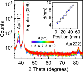
Figure 1. X-ray diffraction patterns obtained at different positions on the substrate. Aside from the (111) reflection of Au, only the c-axis reflections from the substrate are observed. Inset shows the dependence of nanocrystallite size d as a function of position. A linear fit to the data yielded a gradient for the nanocrystallite size of 1.1 Å mm−1.
Download figure:
Standard image High-resolution imageTo accurately evaluate the effective optical constants and thicknesses of the films, the incident angle independent pseudo-dielectric functions were fitted with a three-phase model (air/film/sapphire) including different combinations of a Drude oscillator and Gaussian oscillators, from which the complex dielectric function  as a function of angular frequency ω was determined at each measured sample point:

where ɛ(ω)DO is the complex dielectric function of a Drude oscillator, ɛn(ω)GO the complex dielectric function of the nth Gaussian oscillator obeying the Kramers–Kronig relationship, and ɛ∞ the background dielectric constant. The model parameters (optical constants and thickness) were determined by minimizing the mean squared error.
Figure 2 shows the analyzed optical conductivity which can be broken into 3 regimes, depending on the thickness. All spectra display two features due to the Au d electron interband transitions in the ultraviolet region. For films thinner than tc (figure 3(a)) there are three localized surface plasmon resonances, all of which can be modeled as Gaussian oscillators. As t increases toward tc, one of the plasmon resonances shifts to lower frequency. At tc it transforms into a Drude oscillator, the signature of a free-electron contribution to the conductivity, and it remains so for all larger thicknesses. With further increase in thickness, the two remaining plasmon resonances shift to lower frequency until one of the plasmon resonances disappears at the metal-to-dielectric transition which coincides with the change in sign of the dielectric constant (figure 4).

Figure 2. Frequency dependence of the optical conductivity. Symbols show the different Gaussian–Drude oscillators used to model the optical conductivity in the visible-near infrared region. At t < tc, three oscillators (1, 2 and 3) are required to describe the LSPR contribution. With increasing thickness (tc ⩽ t ⩽ tM), oscillator 2 undergoes a gradual transformation to the Drude oscillator. Moreover, Gaussian oscillators 1 and 3 shift toward lower frequencies as t increases until Gaussian oscillator 3 disappears when t > tM. In all cases, two additional Gaussian oscillators (4 and 5) are also required to describe the Au d electron interband transitions in the ultraviolet region. Plasmon resonances are indicated by red arrows.
Download figure:
Standard image High-resolution imageAs shown in figure 3 (left panel), ε1(0) rose dramatically with increasing t as it approached tc = 7.3 nm, and it then decreased for larger t values, reaching zero at tM = 7.8 nm. From effective medium theory (EMT), one would have anticipated that in going from the dielectric to the metallic regimes, ɛ1(0) would continually decrease with increasing t, in stark contrast to the observations. However, EMT is inappropriate in the critical region as it predicts that sample morphology has a pronounced effect on the optical properties whereas percolation behavior is dependent only on dimensionality. Moreover, in the dielectric region, the nanograins tend to show self-order [2], and scattered fields may add coherently whereby EMT is again inappropriate as disorder is a necessary condition [41].
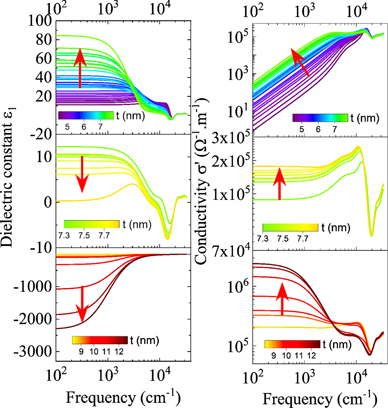
Figure 3. Dielectric constant and optical conductivity obtained from optical measurements for 4.9 nm ⩽ t ⩽ 11.6 nm as indicated by the color maps. Top graphs correspond to t < tc = 7.3 nm, bottom ones to t > tM = 7.8 nm and those in the middle correspond to the percolation region (tc ⩽ t ⩽ tM). The arrows indicate increasing film thickness.
Download figure:
Standard image High-resolution imageAs predicted by classical percolation theory [24, 27, 42] ɛ1(0) (figure 4) obeys the scaling law of equation (1). While these results are similar to those Hövel et al [29, 30], the use of an insulating substrate removes any ambiguity surrounding substrate conduction [20] while the thickness gradient ensures that many measurements can be made, each with a high precision value for the thickness. The fitted value of s ∼ 1 is in accord with the empirical values of the universal law for 3-D networks. The physical origin of the divergence remains unclear although one may postulate that it may be related to hot spots along the percolative path where the electric field becomes greatly enhanced as seen in surface enhanced Raman scattering [43, 44].
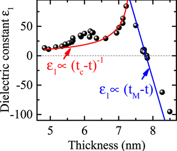
Figure 4. Real part of the static dielectric constant as a function of film thickness t. The solid red and black lines correspond to ε1(0) ∝ (7.3 nm − t)–1 and ε1(0) ∝ (7.8 nm − t), respectively.
Download figure:
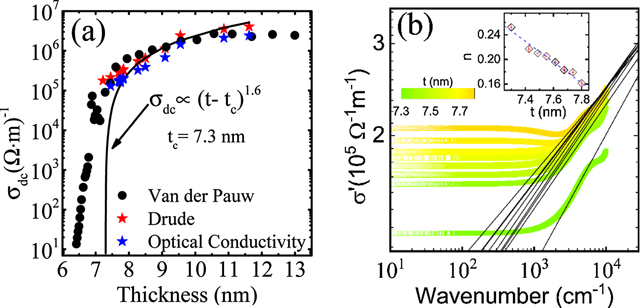
Standard image High-resolution imageFor thicknesses greater than tc, percolation theory [equation (2)] dictates that σdc follows scaling behavior. Near tc, there is fluctuation in σdc (figure 5(a)) as might be expected near the percolation threshold. While σdc decreased by more than 4 orders of magnitude in a very narrow range for t < tc, it deviates from the expected power law relationship because classical percolation theory does not account for TC which becomes more important as t approaches tc.
Figure 5. (a) dc resistivity measured with the van der Pauw method, determined from the Drude equation, and extrapolated from the optical conductivity (figure 3). The full line is the prediction by percolation theory. (b) Log–log plot of σ'(ω) as a function of angular frequency corresponding to the different thicknesses indicated by the color map. Solid lines indicate the fit of the data to a power law with the exponent values shown in the inset.
Download figure:
Standard image High-resolution image
To describe the behavior in the transition region between the dielectric and metallic regimes, we consider the importance of TC [45, 46]. Here we appeal to JUPL to describe the electronic transport in this transition region where tc < t < tM. According to JUPL,

where A is a constant and the exponent n (typically 0 < n < 1) is related to the ratio of the competing electron tunneling/capacitive paths among nanoparticles. For the present case, σ'(ω) obeys the JUPL dependence just above the percolation threshold although the conduction mechanism is dominated by the fractal dimension of percolation clusters [45, 46] rather than well-isolated nanoparticles. Consequently, a combination of both metallic and thermally activated tunneling connections contribute to the conduction.
In order to describe the overall electrical conductivity film, we have considered a random-resistor network [23, 45] consisting of a regular array of cells. Let p denote the probability that two neighboring cells have metallic connections. Consequently, when the metallic cells are densely packed p → 1, and conversely when the cells are isolated from one another p → 0. Accordingly, percolation takes place at critical fraction pc with 0 < pc < 1. To model the ac response, we make the following assumptions: the grains are connected in series by two types of elements, either by (i) metallic resistance RM or (ii) a parallel combination of tunneling resistance Rt and effective capacitance C; and the nanoparticle size is dependent on the thickness but the resistances described by Rt are constant at a given thickness. The values of n found from fitting equation (4) to the measured σ'(ω) relate to the effective fraction of capacitive paths in the network involved in the ac conduction. Since there is an equal fraction of tunneling paths, the resulting exponents n (figure 5(b)) of 0.25 at tc and 0.16 at tM correspond to p = 0.5 and 0.78, respectively, consistent with the results on simulations of random R–C networks [47]. The JUPL regime disappears when the electrical conduction is dominated by electron transport along the meandering and ramified gold interconnected islands [20, 21] as seen in σ'(ω) (figure 3 bottom right).
In summary, we have measured optical constants of an ultrathin film of granular gold with a constant thickness gradient to provide unambiguous evidence of the divergence of the static dielectric constant at the percolation threshold. The dielectric constant be described by scaling laws according to the classical percolation theory while the static conductivity cannot due to the presence of tunneling conductivity. Importantly, for films slightly thicker than the critical thickness, the electronic transport follows Jonscher's universal power law while ε1(0) remains positive even though there is the Drude signature of free charge carriers. Only for larger thicknesses when ε1(0) changes sign does the conduction become metallic.
Acknowledgments
MD acknowledges financial support from Vicerrectorado de Politica Cientifica y Tecnologica (UCA) under grant AC2020-025.