

Abstract
Heterojunction diodes of ZnS/p-Si have been fabricated using the chemical bath deposition (CBD) technique at two different deposition durations under both stirring and non-stirring conditions. The x-ray diffraction (XRD) patterns indicate the deposited ZnS films exhibit good crystallinity with the growth direction along the (111) planes of a cubic zinc blend structure. The crystallite size of all the deposited ZnS thin films have been calculated using the Scherer formula and found to be in the range of 2.2–2.7 nm which is very close (∼4 nm) to the size estimated using transmission electron microscopy (TEM). The surface morphology of the deposited ZnS thin films were studied by scanning electron microscopy (SEM) and it was observed that spherical nanoparticles agglomerated with the increase in deposition time. Furthermore, the optical properties of the deposited ZnS thin films were studied using UV-visible (UV-VIS) and photoluminescence (PL) spectroscopy. The effective calculated band gap was found in the range from 3.7–3.82 eV for all the samples, however PL spectra shows multiple emissions in the as-deposited ZnS films, indicating the presence of intrinsic defects, The characteristics of the fabricated ZnS/p-Si heterojunction diode was studied by measuring the dark current-voltage (I–V) relation using thermionic emission model. Electrical parameters such as barrier height, saturation current, ideality factor and series resistance were extracted from the I–V characteristics of the fabricated Schottky diodes. The barrier potential for all the ZnS/p-Si heterojunction diodes range between 0.829–0.857. Moreover, the calculated ideality factor was found very close to the ideal value of the diode (1.34 and 1.43) in the devices fabricated under stirring conditions.
Export citation and abstract BibTeX RIS
1. Introduction
Zinc sulfide (ZnS) is a prime material of the II–VI semiconductor family. Due to its excellent properties such as large bandgap (∼3.54 eV) [1, 2], comparatively high refractive index with high transmittance in the visible range [3–5] it finds several potential applications such as optoelectronic devices, electroluminescent devices, anti-reflection coating for solar cells, photodiodes, optical sensors and UV LED etc [6–12]. The most important and appealing fact about thin films of ZnS is that it is a non-toxic material; hence is also a suitable candidate to replace the buffer layer of CIGS (Cu (In,Ga)Se2) solar cell device. In most CIGS devices, CdS is used as a buffer layer. But the toxic behavior of CdS stimulated researchers to seek an alternative selection of the material [13, 14]. In this category, ZnS is not only non-toxic but also has a wider bandgap compared to CdS. This property enhances the blue response of the solar cells [15, 16], which considerably increased the efficiency of the CIGS solar cells [17, 18].
ZnS films can be deposited by several physical and chemical techniques. Commonly used techniques are sputtering [19], metal organic chemical vapor deposition (MOCVD) [20], molecular beam epitaxy (MBE) [21], chemical bath deposition (CBD) [22–27], spin coating [28], spray pyrolysis [29], pulsed-laser deposition (PLD) [30] etc CBD is relatively low-cost method but is saddled with the fact that it generates lower quality films as compared to MBE technique. Several studies have been carried out by many research groups, to observe the effect of various parameters such as complexing agent [31], pH [25], annealing temperature [26], etc. on the quality of deposited thin films.
Heterojunction Schottky diodes formed out ZnS thin films deposited on the silicon (Si) -based substrates have reported enhanced electrical properties such as ideality factor, barrier height etc [32]. Since, the lattice constants of Si and ZnS almost match with each other [33], hence ZnS is the best suited semiconducting material for the fabrication of heterojunction diode. Fabrication of n-ZnS/p-Si heterojunction using radio frequency magnetron sputtering was reported by Huang and co-workers [34] and they studied the photo-response of the heterojunction and I–V characteristics at UV and visible wavelengths. Besides, they reported that the heterojunction shows a good rectifying behavior. Wang et al has fabricated ZnS/porous Si heterojunction using PLD technique and discussed the dependence of photoluminescence properties on growth temperature [35]. ZnS:Cr/Si film has been prepared by Nematollahi et al [36] using MBE and PLD techniques and they observed that Cr doping decreases the grain size of the fabricated structures. Ates et al [37] reported the growth of ZnS thin film on n-Si substrate for obtaining Zn/ZnS/n-Si/Au-Sb sandwich structure by using the Successive Ionic Layer Adsorption and Reaction (SILAR) method. Using the I–V characteristics, they calculated the ideality factor, barrier height and series resistance as 2.60, 0.71 eV and 3.8 kΩ, respectively at 300 K. Turgu et al [38] investigated device performance of Al/ZnS/p-Si/Al heterojunction diode which was fabricated using the sol-gel technique. The electrical parameters such as ideality factor, barrier height and the series resistance values were found to be 2.34, 0.77 eV and 12.3–12.5 kΩ, respectively. In one of our recent works [22], we prepared ZnS/p-Si heterostructures at different deposition durations using CBD method. From the study of the electrical performance parameters, we observed improved ideality factor in heterostructure fabricated using 60 min deposition time as compared to 80 min, 100 min and 120 min deposition duration. In our another recent work, we prepared ZnS/p-Si heterostructures using CBD method and fabricated the highly sensitive UV photodetector [39].
From extensive literature study, we observed that most of the thin films based heterostructures were fabricated by ZnO/Si [40], gold—strontium titanate [41], Al/NTCDA/p-Si [42], Zn/ZnS/n-Si/Au-Sb [37], Al/ZnS/p-Si/Al [38] etc. Only scant reports are available in which fabrication of ZnS/p-Si have been studied with the ideality factor close to the ideal value i.e. unity. Most importantly, maximum heterostructures fabricated by other groups use expensive and complex techniques [19–21, 29, 30] as mentioned above. However, we used CBD, which is much simpler than the above-mentioned deposition techniques.
Henceforth, in the present study, we have deposited ZnS thin films on quartz slides and Si wafers via CBD technique at two different deposition intervals (60 min and 80 min) under stirring and without stirring conditions. The effect of stirring and deposition time on crystallinity, surface morphology, and optical properties of deposited ZnS thin films have been thoroughly investigated using XRD, HRTEM, SEM, UV-Vis and PL spectroscopy. The electrical properties have been studied using I–V characteristics and the results have been explained based on the thermionic emission model. Since the field is relatively low, thermionic emission model was used to calculate all essential electrical parameters such as reverse saturation current, barrier height, ideality factor and series resistance.
2. Experimental detail
2.1. Chemical bath deposition
All the essential chemicals of 4N purity have been purchased from Sigma Aldrich (USA) and ZnS thin films were deposited on quartz slides and Si substrates. Prior to the deposition, all the substrates were kept in an ultrasonic water bath for 30 min for cleaning and then again were cleaned using the solution of HCl and acetone for 10 min. Further, they were washed with DI water and dried with a hot air blower. For the deposition of the thin films, a substrate holder was designed in which maximum four substrates (2 Si and 2 quartz substrates) were taken in single deposition experiment. For the preparation of the solution an aqueous chemical bath containing 0.15 M zinc acetate dihydrate [Zn (CH3COO)2,2H2O], 0.3 M thiourea (CS(NH2)2) and 5 M ammonia (NH3) was taken, and the final volume of the solution was kept to 250 ml. The zinc acetate and ammonia were added and mixed in the reaction vessel for 15 min. Thiourea and deionized water were added sequentially to the reaction vessel. During the experiment, the pH was maintained at ∼10 by adding ammonia solution drop wise and the temperature of the solution was kept at 80 °C. During this process, the solution was continuously stirred for 60 min. After complete formation of ZnS, the cleaned quartz and silicon substrates were immersed in the solution in an inclined way. The reaction vessel was completely covered to avoid evaporation. The deposition of the thin film was carried out at constant deposition temperature of 80 °C for two different deposition durations of 60 min and 80 min using both stirring and without stirring conditions. For the deposition under stirring condition, the stirring speed was maintained at 500 rpm. At the end of the deposition experiment, all the substrates were removed from the chemical bath and the deposited ZnS thin films were again kept in the ultrasonic bath for 10 min for washing all impurities. The deposited ZnS films were finally dried in N2.
The samples prepared in this way were named as S60, W60, S80 and W80 (where 60 and 80 denote 60 min and 80 min of deposition time and 'S/W' indicates stirring/without stirring). All the necessary characterizations were performed with these samples. The schematic representation of CBD deposited ZnS thin films is shown in figure 1. The fabrication of ZnS/p-Si heterojunction diode for the I–V measurement is also displayed in figure 1.
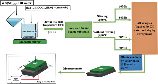
Figure 1. Schematic representation of CBD deposited ZnS thin films and fabrication of ZnS/p-Si heterojunction diode for the I–V measurement.
Download figure:
Standard image High-resolution image2.2. Characterizations
X ray diffraction of the thin films of ZnS were carried out by a glancing incidence (GI) x-ray diffractometer (Rigaku). The operating conditions were as follows: target Cu-kα1, wavelength 1.5418 Å, voltage 40 kV, current 40 mA, scan range: 20°–80°, step size: 0.02°. HRTEM was carried out on JEOL JEM-2100F with an accelerating voltage of 200 kV. Samples for TEM analysis were prepared by drop coating diluted solution on carbon-coated copper grids at normal atmospheric conditions. UV-dual beam Hitachi spectrophotometer was used to obtain the optical transmission spectra in the wavelength range 300−800 nm. PL spectra were recorded using Perkin Elmer LS-55 at an excitation wavelength of 280 nm in the wavelength range 340–500 nm. Surface morphology of the deposited ZnS thin films was observed using SEM (Zeiss cross beam 550).
Current-Voltage (I–V) measurement of the fabricated ZnS/p-Si heterojunction diode was performed using the Keithley 6517 electrometer. Before performing I–V measurements, the ZnS/p-Si heterojunction diodes were coated with silver as a contact material on both sides of the device. All the silver coated ZnS/p-Si heterojunctions were heat-treated at 250 °C for 20 min to ensure better ohmic contact. In the end, a thin copper wires were pasted on both the silver contacts using an electrically conductive paste to connect the device for the measurement.
3. Results and discussions
3.1. Structural properties
3.1.1. XRD studies
The structural property of the deposited ZnS thin films was examined by XRD analysis. Figure 2 shows the XRD patterns of all the ZnS thin film deposited with and without stirring condition at 60 min and 80 min duration. It can be observed that the deposited ZnS films exhibit cubic phase with diffraction peaks at 2θ∼28.83°, 48.6° and 57.33°, which correspond to the (111), (220) and (311) planes of the cubic zinc blend structure (JCPDS, No. 05-0566) respectively [43]. A clear peak is observed at 2θ∼51.25° is due to the Si substrate, which has been used as a substrate for the ZnS/p-Si heterostructures. From figure 1, it is also clear that the peaks are broadened which represents the nanocrystalline behavior of the particles.
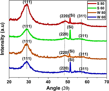
Figure 2. X-ray diffraction patterns of ZnS thin film deposited on Si substrate (a) S 60 (b) S 80 (c) W 60 (d) W 80.
Download figure:
Standard image High-resolution imageThe average crystalline size (D) was calculated for the deposited thin film using the well-known Scherer formula [44]. For the calculation of crystallite size, we considered the most intense peak (111) from XRD patterns of the ZnS.

where k (=0.9 for spherical particles), λ is the x-ray wavelength used (=0.154 nm), β and θ are the full-width half-maxima and the Bragg's diffraction angle of the highest intensity peak of (111) plane, respectively. The calculated values of the crystallite size for all the deposited thin films are shown in table 1 and found to be in the range of 2.2–2.7 nm. It can be noticed from table 1, the crystallite size slightly decreases with increase in deposition duration under both stirring and without stirring conditions.
Table 1. Calculated Lattice constants, crystallite sizes, dislocation densities and band gaps of the deposited ZnS thin films.
| Lattice constants | ||||||||
|---|---|---|---|---|---|---|---|---|
| Sr No. | Sample | Interplanar spacing (d) in nm | Cell parameters (a) in nm | Crystallite size (D) using XRD pattern (nm) (±0.1 nm) | Dislocation density δ (m−2) | Band gap (eV) (±0.05 eV) | Blue shift w. r. t. Bulk (ΔE) | Urbach energy (eV) (±0.02 eV) |
| 1. | S60 | 0.3098 | 0.5359 | 2.7 | 12.9 × 10¹⁶ | 3.7 | 0.16 | 0.235 |
| 2. | S80 | 0.3094 | 0.5352 | 2.5 | 15.3 × 10¹⁶ | 3.73 | 0.19 | 0.34 |
| 3. | W60 | 0.3092 | 0.5349 | 2.4 | 17.3 × 10¹⁶ | 3.79 | 0.25 | 0.502 |
| 4. | W80 | 0.3106 | 0.5373 | 2.2 | 20.6 × 10¹⁶ | 3.82 | 0.28 | 0.513 |
Further, we calculated dhkl which is the interplanar spacing of the lattice (= λ/2sinθ) and the comparative analysis is shown in table 1.
Lattice parameter (a) was calculated using the formula,

where, h, k, and l are the Miller indices of the lattice plane.
From table 1, it can be elucidated that calculated interplanar spacing and lattice parameter are found in the range of 0.3092 nm–0.3106 nm and 0.5349–0.5373 nm, respectively. The calculated values of both the parameters are well in agreement with the previously published reports [39, 45–47].
The dislocation density (δ) is defined as the 'length of dislocation lines per unit volume of the crystal, which is the size of the crystal defects possessed by a crystal' and higher values of 'δ' indicate lower crystallinity levels for the films. Hence, the dislocation density value will illustrate the degree of crystallinity of the nanoparticles. The dislocation density was calculated using the well-known Williamson & Smallman relation [48].

where D is the average crystallite size and calculated results are summarized in table 1. The dislocation density was found to be high, and this was ascribed to the extremely small sizes of the crystallites.
3.1.2. Transmission electron microscopy
Figure 3 shows the transmission electron micrograph of the sample S60 and the inset shows the selected area electron diffraction (SAED) pattern. ZnS has a poor contrast in electron microscopy but the particles in the form of lattice planes are clearly visible under high magnification. We have indicated the particles with which circle to discern them easily. The average particle size is ∼4 nm which is close to the sizes estimated from the Scherrer equation. The SAED pattern shows the (111) and (220) planes clearly which indicates the formation of the ZnS crystal structure. But the width of the circles in SAED and their slightly diffused intensity is indicative of the poor crystallinity of the films formed.
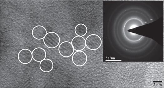
Figure 3. HRTEM image of the sample S 60. Inset shows the corresponding SAED pattern.
Download figure:
Standard image High-resolution image3.2. Optical properties
3.2.1. UV-visible spectroscopy
The optical transmittance has great importance in semiconductor for various applications. Figure 4(a) shows the optical transmission spectra of all the ZnS thin films. The transmission spectra of all the deposited thin films were recorded in the wavelength region of 300 nm to 800 nm. It can be seen from figure 4(a), that the transmittance of the samples S60 and W60 is higher compared to the samples S80 and W80. Since, increase in deposition time increases the thickness of the thin films, this results in decreasing the transmittance. Also, stirring provides uniformity in the deposition of thin films which obviously improves the quality and hence increase the transmittance compared to W60.

Figure 4. (a) UV-visible transmittances (b) tauc plots of all the ZnS samples.
Download figure:
Standard image High-resolution imageFigure 4(b) shows the plot between (αhν)2 and photon energy (hν) for the determination of bandgap of the deposited thin films. The bandgap was calculated using the Tauc's relation [49] for zinc sulfide which is a direct bandgap semiconductor.

where A is the constant, α is the coefficient of absorption,  is the photon energy,
  is the optical band and the value of n = ½ for the direct band gap semiconductors. The effective band gap calculated from Tauc relation for S60, S80, W60, W80 samples are 3.7, 3.73, 3.79, 3.82 eV, respectively which is higher in comparison to the bulk ZnS band gap (3.65 eV). The shift in the bandgap of the ZnS thin films could be associated with the quantum effects, mostly due to the presence of small crystallites in bigger grains and defect levels. Since, the bulk ZnS shows the Bohr exciton radius of ∼2.5 nm and in the present study the calculated crystallite size was found in the range 2.2–2.7 nm, which is in the vicinity of Bohr exciton hence they exhibit excitonic confinement [39].
3.2.2. Absorption band tail (Urbach energy)
Semiconductors generally show strong absorption in the band gap region. Generally, for materials which are poorly crystalline, an exponential part in the optical band edge is observed and is referred to as the Urbach tail. This energy tail is a consequence of localized states penetrating into the band gap region. The Urbach experiential rule is given by

where  is a constant and EU denotes the Urbach energy. Taking log on both sides we get

So, the Urbach energy can be obtained from the slope of straight-line plot of  versus the incident photon energy. Figure 5 shows the variation of EU with the band gap obtained for the different samples under study. We see that the Urbach energy is lower for the samples prepared under stirring condition as opposed to those prepared without stirring. This is expected as stirring leads to more homogeneous and equilibrated growth which leads to better crystallinity and lower disorder. Such a variation can also be successfully explained based on the Mott and Davis model [50] applicable for disordered materials.

Figure 5. Dependence of the optical band gap, Eg with Urbach energy, EU of all the samples.
Download figure:
Standard image High-resolution image3.2.3. Photoluminescence studies
The PL spectra of all the samples are shown in figure 6(a). The PL study gives a mapping of the native point defects present in the sample. In addition to these point defects, surface states can also act as active sites adding to the possibility of photo-transitions. ZnS having the cubic zinc blende structure has predominant presence of Schottky defects [51]. Figure 6(b) shows the band diagram to show various transitions observed in the PL spectra.
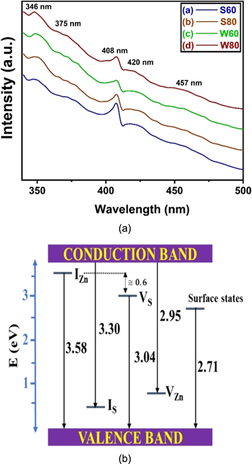
Figure 6. (a) Photoluminescence spectra of all the ZnS samples (b) Band diagram showing various transitions of Photoluminescence spectra.
Download figure:
Standard image High-resolution imageThe prominent peaks obtained from the PL spectra are located at 346 nm, 408 nm and 420 nm. Additionally, small humps with low intensity and wider spread are noticed to be centred at 375 nm and 457 nm. The peak at 346 nm is ascribed to transitions from the zinc interstitial (IZn ) levels to the valence band edge. The IZn acts as a shallow donor level due to the low binding energy of the electrons. It acts as an efficient trapping centre for electrons just below the conduction band albeit having sufficient energy difference with the conduction band edge to stop de-trapping due to thermal excitations. The peak at 408 nm is assigned to transitions from the neutral sulphur vacancy levels (VS ) to the valence band edge. VS is amphoteric and the position of Fermi level determines whether it behaves as an acceptor or a donor. In our case, due to the presence of IZn , which is a donor, the sample behaves like an n-type semiconductor pushing the Fermi level towards the conduction band edge.
In fact, we observe that inspite of the amphoteric nature of VS , it behaves as a donor level in our case, separated from the IZn levels by an energy of about 0.6 eV. The peak at 420 nm is due to transitions from the conduction band edge to the zinc vacancies (VZn ). The VZn produce acceptor levels and theoretical calculations have predicted that depending on their charge states, they are placed between 0.5 eV to 1.1 eV above the valence band edge [52]. The small hump at 375 nm is ascribed to the transitions from the conduction band edge to the levels arising out of sulphur interstitials (IS ). Although IS is amphoteric, yet for an n-type semiconductor, they behave as acceptor levels and theoretical calculations have shown that these levels are placed at around 0.6 eV above the valence band edge. This provides a good match with the transition we have seen in our PL spectra. Notably, the intensities of transition arising from VZn and IS levels are much weaker due to the n-type character of the semiconductor which promotes the donor impurities vis-à-vis the acceptor impurities. The hump centred at 457 nm is ascribed to the transitions from the levels arising out of the surface states and dangling bonds to the valence band edge [53]. Nanoparticles have enhanced surface to volume ratio and the surface always has unsaturated bonds and defects due to the result of the sudden termination of the lattice periodicity. But the low intensity of the hump assures the fact that the concentration of such defects in our sample is very small.
3.3. Scanning electron microscopy
Surface morphology of the deposited ZnS thin films were studied by SEM. Figures 7(a)–(d) depict SEM images of ZnS thin films deposited for 60 min and 80 min duration under stirring and without stirring conditions. All the deposited ZnS films are uniform and have spherical morphology of the ZnS particles. The effect of the deposition time can be clearly seen on the surface morphology for both stirring and without stirring conditions. Figures 7(b) and (d) reveals that spherical nanoparticles agglomerate with increase in deposition time. It can be observed from SEM images that higher substrate coverage has been achieved at higher deposition time, which is a key part for any device. During comparative observation, we found that thin films deposited under stirring condition (S60 and S80) shows better surface uniformity or homogeneity than those deposited without stirring (W60 and W80). From figures 7(a)–(d) one can also observe that the ZnS thin films deposited at higher deposition duration show more compact nature as compared to other two ZnS thin films. Such dense film is most essential for the charge carrier transportation when utilized in solar cell as a buffer layer.

Figure 7. SEM image of the ZnS thin film deposited on Si substrate (a) W 60 (b) W 80 (c) S 60 (d) S 80.
Download figure:
Standard image High-resolution image3.4. Electrical studies
The schematic representation of the experimental arrangement to determine the electrical performance parameters of the fabricated Schottky diode is shown in figure 8. The dark I–V characteristics performed at room temperature and their corresponding results are shown in figure 9. The I–V characteristics recorded between −5 and 5 V of the ZnS/p-Si heterojunction diode indicate the Schottky nature of the diode. By using the I–V characteristics, critical electrical parameters of the Schottky diode such as reverse saturation current (Is ), barrier height (Φb), ideality factor (η) and series resistance (RS ) have been evaluated.
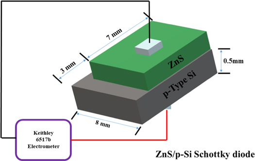
Figure 8. Schematic representation of the experimental arrangement for the measurement of J–V using the fabricated heterojunction ZnS/ p-Si Schottky diode.
Download figure:
Standard image High-resolution image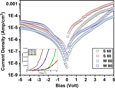
Figure 9. The experimental J–V curves of heterojunctions fabricated using different ZnS thin films at room temperature. The inset shows linear I versus V of the same heterojunctions under forward bias condition.
Download figure:
Standard image High-resolution imageThe Schottky diode charge transport mechanism have been explained by a thermionic emission model [54] which can be written as

Here, IS is the reverse saturation current, which is given by the following relation.

where  is the barrier height at zero bias, q is the electronic charge, V is the applied voltage, A is the diode area, A* is the Richardson constant, η is the ideality factor, k is the Boltzmann's constant and T is absolute temperature. The equation may be re-framed in terms of barrier height as

IS
can be evaluated by extrapolating the semi logarithmic I–V plot such that it intercepts the current axis at V = 0. The value of barrier height  for the Schottky junction was calculated using equation (9). The results are summarized in table 2. It can be noticed that the barrier potential for all the ZnS/p-Si heterojunction diodes ranges between 0.829–0.857. Among all four, ZnS/p-Si heterojunctions fabricated using stirring conditions (S80 and S60) have lower barrier height in comparison to the junctions fabricated using without stirring conditions (W80 and W60). This indicates that the quality of ZnS thin films improved under stirring condition. Subsequently, the calculated reverse saturation current was obtained in the range 6.4 × 10⁻⁹ A to 1.93 × 10⁻⁸ A.
Table 2. Calculated I–V parameters of ZnS/p-Si heterojunction diode.
| Sample name | Barrier height  (eV) (eV) | Saturation current  (Amp) (Amp) | Ideality factor ( ) ) |
 (kΩ) by dV/d(lnI) slope (kΩ) by dV/d(lnI) slope |
|---|---|---|---|---|
| S60 | 0.829 | 1.93 × 10⁻⁸ | 1.34 | 3.6 |
| S80 | 0.834 | 1.56 × 10⁻⁸ | 1.43 | 3.0 |
| W60 | 0.857 | 6.4 × 10⁻⁹ | 2.75 | 7.7 |
| W80 | 0.845 | 1.04 × 10⁻⁸ | 5.22 | 4.0 |
Using equation (7), the ideality factor can be calculated by the equation as

Ideality factor of the fabricated ZnS/p-Si heterojunctions was calculated using equation (10) and the results are tabulated in table 2. The ideality factors for the ZnS/p-Si heterojunctions fabricated using S60 and S80 were found to be 1.34 and 1.43, respectively. However, in other two samples i.e. W60 and W80, the ideality factor was observed to be 2.75 and 5.22. For an ideal diode, ideality factor equals to unity, but in real conditions it may be higher than the ideal value. Hence, for the samples S60 and S80, it is very close to the ideal value of the diode. However, for the other two samples W60 and W80, the value of the ideality factor increases and the increase in ideality factor is attributed due to many reasons such as (i) presence of oxide layer between interface of thin film and substrate i.e. interfacial defects (ii) series resistance (iii) leakage current and (iv) low fill factor.
The values of ideality factor close to unity signify the existence of both diffusion current and recombination current. Also, it has been reported that reduction in fill factor causes higher value of ideality factor [55]. This is consistent with our observation that thin films deposited under stirring conditions have better substrate coverage i.e. fill factor as compared to without stirring conditions.
Series resistance is an important electrical parameter of the Schottky diode, which limits the flow of current in the device. To investigate the series resistance, Cheung and Cheung's method [56] was used; as Cheung's function is given by

where, RS
is the series resistance. To calculate the series resistance, a graph between  versus I was plotted for all ZnS/p-Si heterojunctions and is shown in figures 10 (a)–(d). The graph shows a straight-line behavior for a low ordinate cut-off, and the value of series resistance was calculated using the slope of the plot. The calculated values of series resistance are shown in table 2; it can be noticed that the series resistance is smaller for S80 and S60 samples compared to the W80 and W60. The probable reason for high series resistance in W80 and W60 may be due to higher concentration of interfacial defects and a poor fill factor [56].

Figure 10. dV/d (lnI)-I plots of heterojunctions fabricated using different ZnS thin films at room temperature.
Download figure:
Standard image High-resolution image
4. Conclusion
ZnS/p-Si Heterojunction Schottky diodes were successfully fabricated using CBD technique. The XRD reveals that thin films are nanocrystalline and monophasic with wurtzite crystal structure. The calculated crystallite size using the Scherrer equation was found to be in the range 2.2–2.7 nm which is very close to the size estimated by TEM images. Besides, the SAED pattern confirmed the cubic zinc blend structure of the deposited ZnS thin films. Using the absorption spectroscopy analysis, the calculated band gap of the samples observed in the range 3.7–3.82 eV while the calculations of Urbach energy confirmed that the disorder in the samples without stirring was greater than the samples prepared under stirring condition. Morphological analysis via SEM confirms the the ZnS thin films deposited at higher deposition duration show more compact nature as compared to other two ZnS thin films. Further, PL spectroscopy revealed the signature of the native defects of ZnS. The electrical performance parameters reveal fabrication of ZnS/p-Si base heterojunction diode using thin film prepared under stirring conditions leads to much better ideality factor (1.34 & 1.43) which is very close to ideal diode. Hence, we may conclude that ZnS thin films grown with CBD technique with stirring, can effectively replace other possible candidates for UV detector applications.
Data availability statement
All data that support the findings of this study are included within the article (and any supplementary files).
Compliance with ethical standards
Conflict of interest
The authors declare that they have no conflict of interest.