

Abstract
This paper presents the results of experimental studies of switching processes of high-temperature superconducting tapes under the action of a pulse current load of microsecond duration. The reversible, stable and irreversible switching of the superconductor to the normal state has been realized. To demonstrate the opportunity of controlled generation of transients in superconducting composites, the characteristics of a superconducting switch capable of cyclic switching between flux flow and ohmic modes with preservation of switching parameters were investigated. The characteristics of a superconducting switch have been calculated based on experimental results.
Export citation and abstract BibTeX RIS
1. Introduction
The opportunity of nearly dissipation-free transmission of electric power using superconductors makes it possible to significantly increase the efficiency of power systems [1]. Nowadays, high-temperature superconducting (HTS) tapes are increasingly finding applications in the fields of the energy industry, energy-efficient systems for transmission, storage, distribution and distribution of energy [2–4]. The realization of pronounced thermally-induced dynamic states (TDS) leading to the transition of the superconductor to the normal state allows the application of HTS tapes in such devices as current limiters [5] and HTS switches (keys) [6]. The actuation rate of such HTS switches is generally limited by the rate of heat propagation and the normal zone. Several works [7–11] have been devoted to investigations of the processes of formation and movement of the normal zone, quench development, and also heating of the superconductor under current pulses in the range of current-rise times from tens of microseconds to hundreds of milliseconds. The physics of the development of thermal processes in superconductors in such loading regimes is well studied, and its description is reduced to the models of magnetic flux flow and creep [12–14]. The obtained characteristic normal zone propagation velocities in HTS tapes are in order of a few cm/sec, and heating can reach hundreds of kelvins [15].
It was shown in the papers [16–19] that at milliseconds current actions there is a strong influence of liquid nitrogen boiling modes, dynamic heating processes and hot spot formation on the measurement results, which, in turn, significantly complicates the processing and interpretation of experimental data, as well as simulation of such systems. Shorter current pulse times are required to study fast physical processes not related to the heat spot propagation [20]. Presumably, a number of other factors such as rising edge rate, cooling regimes and sample geometry can also have a significant effect on HTS sample switching processes. Thus, in paper [21], at supercritical current loads with the duration of the rising edge of ∼10 μs, the shift of the thermal transition threshold was demonstrated for YBa2Cu3O7-x (hereinafter YBCO) samples with different thicknesses of shunt metal layers. Within the framework of [21], three modes of current flow I through a superconductor are considered: the magnetic flux creep mode at I < Icr , the magnetic flux flow mode at Icr < I < I* , and the ohmic mode at I > I*. In this case, under a pulsed current load of microsecond duration, the value of the current at which the transition from the flux creep regime to flux flow, Icr , is observed differs from the nominal Ic of the superconductor obtained by slow volt–ampere characteristics (VAC) measurement. This is due to the influence of thermally induced dynamic states arising in the superconductor under short current actions and indicates the existence of a critical thermal transition current, which was also found by us in [22] under current pulses of millisecond duration. Moreover, all three current thresholds (Icr , Icff , I*) shift as the sample geometry changes.
The shift in current switching thresholds, which depends on a large number of factors, prevents the prediction of the performance of HTS switches based on first-principles approaches. However, using basic experimental techniques such as current and voltage measurements on the HTS sample during current load application, it is possible to unambiguously establish the boundary modes of operation of a HTS key of a given architecture in given cooling and loading regimes. This allows to carry out precise control over the processes of TDS development in HTS composite tapes. Thus, the main purpose of the present work is to demonstrate the possibility of obtaining stable switching of the HTS composite and to calculate, based on the analysis of the dynamic resistance of the HTS layer, the parameters of cyclic switching of the superconductor between different types of terminal excitations (switching of the circuit power supply between a current source and a voltage source). In particular, when determining the cut-off current and voltage based on experimental results, it is possible to predict the switching parameters of the HTS element, which will not lead to superconductor overheating and development of irreversible transition to the normal state, i.e. the HTS key will continuously operate as a switching relay. Such HTS switches, due to their ability to repeatedly change the circuit supply parameters between low voltages and high transport currents, will find applications in energy systems such as kinetic and induction energy storage, HTS motors and generators [1, 3, 6, 23].
The paper is structured as follows: section 2 describes the samples for experimental studies and the experimental technique itself for measuring current and voltage on the sample under supercritical pulsed current loading with a rising edge time of 2 μs or less. Section 3 describes the numerical models that are used to process the experimental results and allow the calculation of the dynamic resistance of the HTS layer, as well as the prediction of the parameters of the HTS switch as part of an electrical circuit. Section 4 presents the results of experimental studies, reveals three main operating modes of HTS composites under given cooling and loading conditions, and establishes the parameters of the 'cruising' load - the value of transport current at which stable switching of the sample is observed, i.e. the voltage on the sample remains constant at a constant current load. Based on the obtained information on the boundary modes of operation of the HTS element, simulation of the processes of cyclic switching of the commutator between a DC source and a DC voltage source (switching between types of terminal excitations) is performed.
2. Experimental details
The specially made automated experimental stand with a pulsed current source was used to carry out transport measurements when short electric current pulses were passed through the HTS sample. The circuit diagram of the current source is shown in figure 1. The principle of operation of the source is based on a fast transient process at discharge of a chain of capacitors of large capacitance (12 capacitors, 4700 μF each). schematic diagram of the current source. The experimental stand also includes voltage amplifiers to increase the sensitivity of the oscilloscope. The operation of the source is controlled by a programmable logic circuit based on the Arduino Due microcontroller. Generation of a single pulse is performed in two stages: capacitor charging and subsequent discharging, which creates a rectangular pulse with a controlled length of 7 μs to 500 μs and a rising edge time of 1–5 μs. The maximum current amplitude in the pulse is 1.5 kA (when charged to a voltage of 50 V). Electrical measurements were carried out in liquid nitrogen using a four-terminal method. The distance L between the potential contacts, at which the voltage measurement on the sample was carried out, was 8 mm. Such an interval was chosen for the reasons of forming a stable current pulse at small exposure times and minimising the influence of dynamic heating processes, hot spot formation and liquid nitrogen boiling modes on the measurement results.
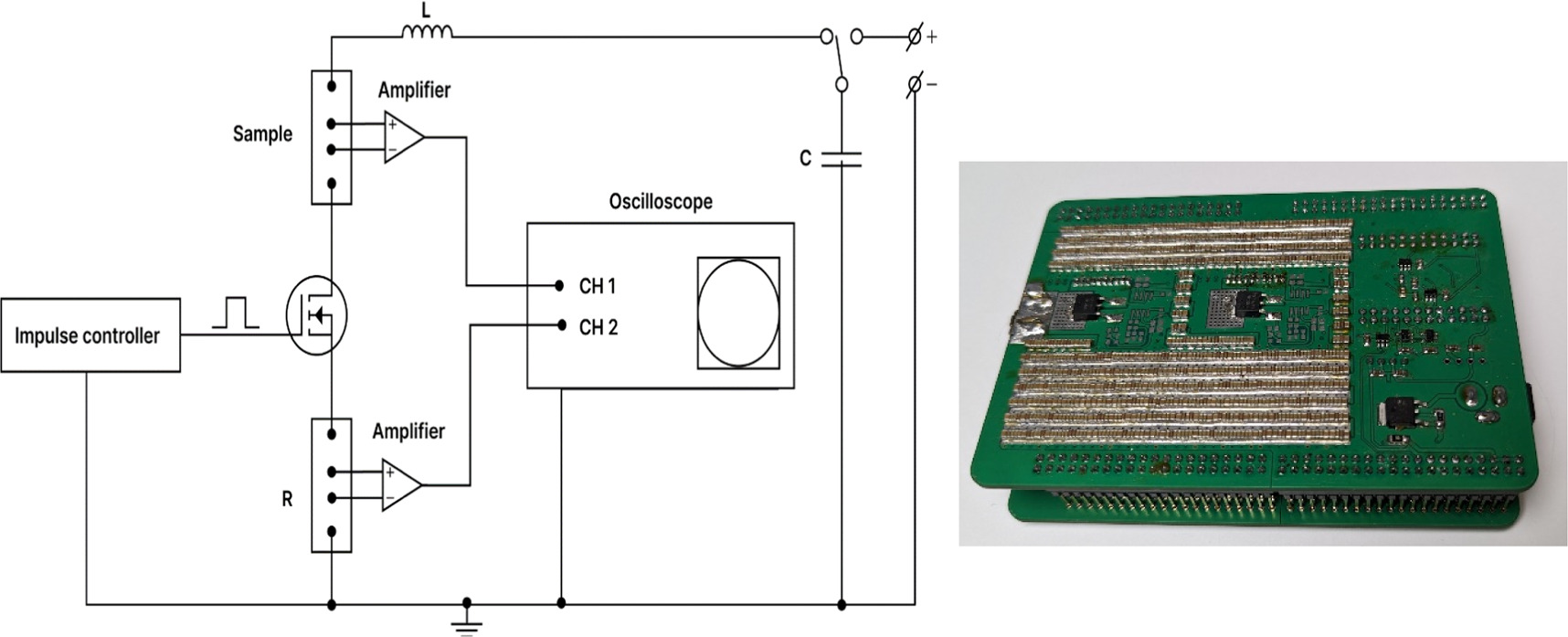
Figure 1. Circuit diagram of a pulsed current source. Photo of a pulse current source.
Download figure:
Standard image High-resolution imageCommercial HTS tapes manufactured by SuperOx with a width of 4 mm containing 40 μm thick Hastelloy C276 alloy substrate layers , 1–3 μm thick YBa2Cu3O7-x HTS layer, silver layer (∼3 μm), and double-sided copper coating (∼20 μm) were used as samples for experimental studies. The critical current Jc of HTS tapes in its own field at the boiling point of liquid nitrogen was 120 A. The experimentally measured critical temperature of HTS composite was 92 K. The samples cooled with liquid nitrogen were exposed to transport current pulses of amplitude up to 600 A (5 Jc ). The duration of the current exposure is 100 μs, and the rise time of the rising edge does not exceed 2 μs.
3. Numerical simulation
To demonstrate the peculiarities of controlling the switching processes of HTS composites, a switching device model was developed to control the circuit power supply parameters, in particular the possibility of simultaneous current and voltage power cut-off. Several new simulation approaches were used for the model implementation of the HTS switch. It is well known that at short current loads, the resistance of HTS cannot be analyzed using the classical method of calculating the step dependence for the CVC of the HTS [24, 25]. The necessity to take into account the dynamic resistivity of the superconductor at the leading edge of the current action at pulsed current actions was previously reported in the literature [26, 27]. Within the framework of the presented work, the previously proposed and verified dynamic resistance model [28] is used to analyze resistances at temperatures below the onset temperature of the N-S transition. The model takes into account the cooling modes of the system and uses experimental data on voltage and current on the sample as input parameters, which allows us to trace the processes of current redistribution between the layers of HTS composites. The most important results of such a calculation are time dependences of the dynamic resistance of the HTS layer for a particular loading mode, as well as time dependences of the heat sink power for a given cooling mode. It should be noted that the dynamic resistance model is not independent - it uses and processes experimental data, allowing to calculate characteristics that are not directly evident from the experiment, namely time dependences of resistances of all tape layers. In order to investigate the switching behavior of HTS tape in an electrical circuit and to recover the magnitude of total current and current in the superconducting layer, a model based on an equivalent electrical circuit was developed. The calculation circuit is shown in figure 2.

Figure 2. Calculation scheme for simulation of the HTS tape under current. The following designations are adopted in the circuit diagram: C — capacitor bank, Rs — shunt resistance, Ls — shunt inductance, Rall — total circuit resistance, including resistance of wires, contacts, etc, Lall — total circuit inductance, Rsc — resistance of the superconducting layer, Lsc -— the inductance of the superconducting layer, Rcu — resistance of the resistive layer of HTS tape, Lcu — inductance of the resistive layer of HTS tape.
Download figure:
Standard image High-resolution imageIt is assumed that capacitor C is charged to a fixed value and the key is closed at the initial instant of time. As a result of the capacitor discharge, a current pulse is formed through the superconductor. The calculated scheme does not reflect all components of the current source elements. In order to account for inductive processes in resistive circuit elements and wires, the main components on which measurements are made in the experiment are represented as series resistance and inductance. The remaining resistances (wires, etc) and resistors in the current source circuit were combined to form the total resistance of the circuit and the total inductance of the circuit. The values of total resistance and inductance were obtained from experimental data, the shunt resistance matches the manufacturer's stated value. The superconducting tape was presented as a parallel connected HTS tape and an effective resistive layer (substrate, silver, copper). The resistances of the resistive layers are known, and the resistance of the HTS layer is set based on the results of the analysis in the dynamic resistance model. The inductance has been added to account for the circuit parameters when the current changes rapidly. The diagram also shows measuring devices (ammeters and voltmeters), which can be used to track the current redistribution, voltage changes on the shunt and HTS tape, as well as to analyse the effect of the inductive contribution on the signals measured in the experiment. The circuit calculation was performed in Comsol Multiphysics environment.
Verification of the numerical model at this stage was performed by comparing the experimental and calculated total currents in the circuit (figure 3).
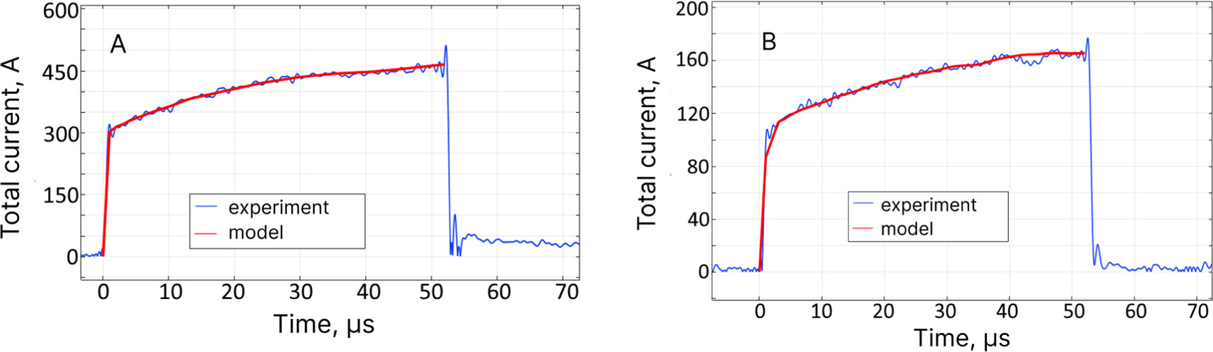
Figure 3. Experimental and calculated dependencies of total current in the circuit at different amplitudes of rectangular current pulse (A) at J ∼ 3.7 Jc, (B) at J ∼ 1.3 Jc.
Download figure:
Standard image High-resolution imageA numerical model of a switching HTS device for analysing cyclic switching of a HTS element has been developed on the basis of the Electric currents module of the Comsol Multiphysics package with integration of the Events interface into the model and shows the possibilities of using a HTS switch for controlling consumer power supply parameters. A similar approach was applied to calculate the switching parameters of a copper conductor with an initially known constant resistance [28]. In the case of HTS switch performance prediction, the properties of the HTS element are dynamic and the resistance is determined by the load and cooling parameters. In addition, switching is realised between a constant low voltage source and a constant high current source. This means that the HTS key is able to monitor small voltage changes and switch to DC mode with lower voltage values, thus fulfilling the function of protecting the circuit from overheating.
The operating mode of a HTS key as part of a switching HTS device should correspond to the boundary of irreversible growth of resistance (and, hence, of voltage), i.e. the HTS key should be at the threshold of development of dynamic thermal instability. This means that the HTS key must pass such a current, above the value of which the resistance of the HTS element will increase even when a constant transport current is flowing. The Events interface discrete state function defines a single state variable S that acts as a marker indicating whether the power supply is in DC mode S = 1 or DC voltage mode S = 0. Then there is an indicator state function that defines two variables Uthr (threshold voltage) and Jthr (threshold current) to change smoothly over time. Finally, there are two implicit event functions that will monitor these two indicator state variables and change the discrete state variable S to zero or one. The voltage switching process at constant current is controlled by the HTS key, for which the transition to the resistive state (resistance increase) starts when the set cut-off voltage is exceeded. The resistance of the HTS layer is calculated from experimental data in the dynamic resistivity model, and the current in the superconducting layer is recovered from the equivalent circuit model. Thus, the switching HTS device model only predicts the behaviour of the HTS key for experimentally determined transient current and voltage values on the sample.
4. Results and discussion
Using the described pulsed current source, we carried out a series of experimental studies on exposure of the HTS sample to transport current pulses of amplitude from 1 to 600 A (5 Jc ) with pulse duration of 100 μs and rise time of the exposure front not more than 2 μs. Recall that the critical current of HTS composites at the boiling point of liquid nitrogen is 120 A. Based on the results of a series of experimental studies, the dependence of the maximum voltage on the HTS sample on the amplitude of the applied transport current was plotted (figure 4).

Figure 4. Dependence of the maximum voltage value on the superconductor on the current amplitude. The critical current of the sample is 120 A, the pulse duration is 100 μs, the rise time of the exposure front is 5 μs.
Download figure:
Standard image High-resolution imageFor convenience, the amplitude of the applied current is normalised by the value of the critical tape current. The presented dependence is approximated with good accuracy by two linear functions. At transport current amplitudes up to ∼1.8 Jc , a low impedance voltage mode or so-called flux flow mode is observed. Another linear switching mode, defined as ohmic switching mode, starts at current amplitudes above ∼2 Jc . Noteworthy is the fact that at such short rise times of the current front, even at currents below the critical current, the nonlinear mode of magnetic flux creep reported for longer current loads is not observed [21]. The presence of resistivity of the superconducting layer at the leading edge of the current action causes that at any non-zero current, the magnetic vortices come into motion and a voltage on the sample is generated.
The appearance of stress on the sample in any case indicates the formation of a pronounced TDS, the beginning of the development of thermal instability of the system and switching of the superconductor to the normal state. The difference between the flow regime and the ohmic regime lies in the dynamics of the TDS development during pulse application. The low-resistance mode corresponds to reversible switching of HTS composite to the normal state and is characterised by a decrease in the voltage across the sample while keeping the transport current constant or even increasing. Figure 5 shows, as an example, the experimental time dependences of current and voltage on the sample under a current pulse of amplitude slightly higher than the critical composite current. The maximum increase in voltage, and hence heat generation, is observed during the current pulse injection process. For 2 μs, a current of 110 A was injected into the sample, which corresponds to a current injection rate of 220 MA/s. Due to the peculiarities of the experimental bench, after 2 μs the injected current continues to grow slowly, reaching a value of 140 A at the final moment of time. In spite of this, the degree of heat generation during slow current growth becomes less intense than during the initial pulse injection process. The heat generated at the initial stage is dissipated into liquid nitrogen, and the continued heat generation only slightly affects the transport characteristics of the composite. Because of this, the sample voltage begins to drop as the current load continues. For any current amplitudes less than 1.8 Jc , the voltage begins to drop before the end of the transport current application. The second linear mode, or ohmic mode, is characterized by continuous voltage growth up to the end of constant current load application (figure 6).
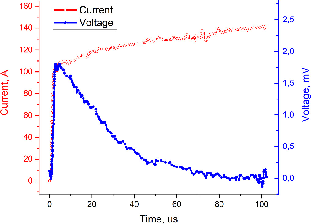
Figure 5. Time dependences of current and voltage on the HTS tape sample when a current pulse of 140 A amplitude (∼1.17 Jc,) is applied. The duration of the current load is 100 μs, the rising edge rise time is 5 μs. Reversible switching.
Download figure:
Standard image High-resolution image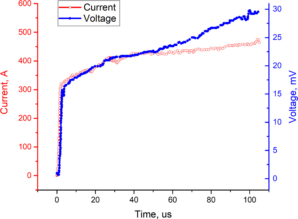
Figure 6. Time dependences of current and voltage on the HTS tape sample when a current pulse of 450 A amplitude (∼3.75 Jc) is applied. The duration of the current load is 100 μs, the rising edge rise time is 5 μs. Irreversible switching.
Download figure:
Standard image High-resolution imageIn the ohmic mode of magnetic flux flow, irreversible switching of the superconductor is observed, which, under continued current load, will inevitably lead to thermal destruction of the sample.
There is a sufficiently narrow region of transport currents between the flux flow regime and the ohmic regime in which a stable switching regime is observed (figure 7). In this regime, the heat generation and heat dissipation processes in the system are balanced and the sample voltage is maintained at approximately the same level throughout the pulse, despite the fact that the transport current exceeds the critical composite current by almost a factor of two.
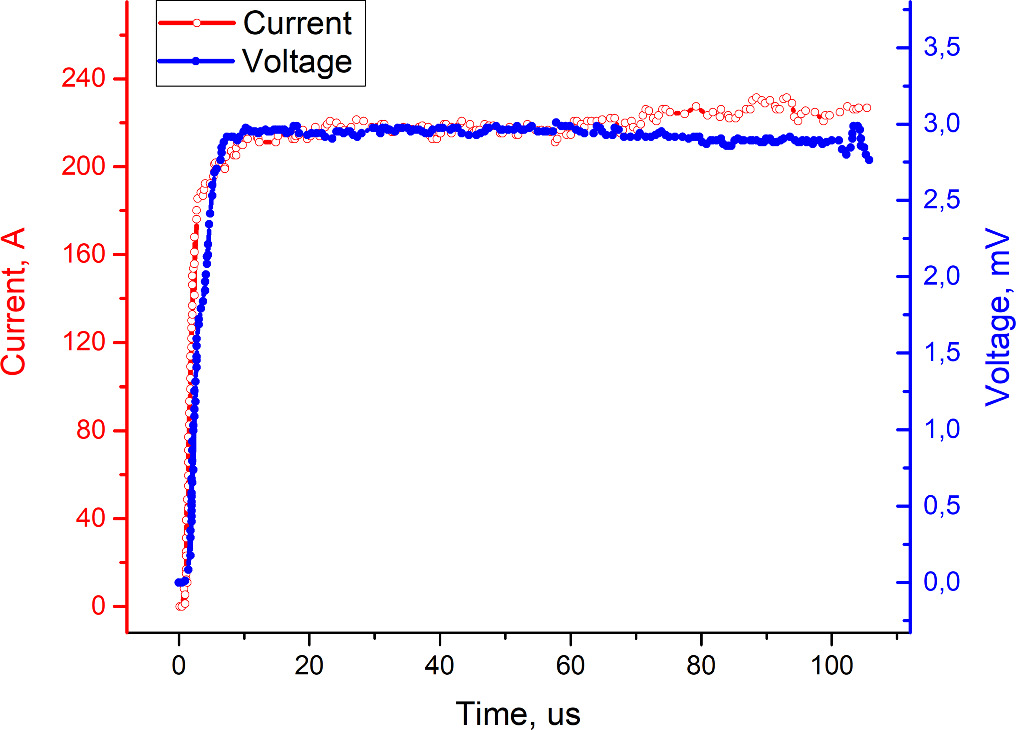
Figure 7. Time dependences of current and voltage on the HTS tape sample when a current pulse of 231 A amplitude (∼1.93 Jc) is applied. The duration of the current load is 100 μs, the rise time of the effect front is 5 μs. Stable switching.
Download figure:
Standard image High-resolution imageThe balancing processes between the thermal processes in the system are influenced by the load and cooling modes as well as the architecture of the composite HTS tapes, such as the thickness of the stabilising layers. However, the ability to experimentally detect stable superconductor switching allows us to determine the peak voltage Umax peak voltage amplitude Jmax peak current values and apply them to the development of a switching HTS device. When these thresholds are exceeded, the development of TDS in the system becomes uncontrolled. When a pulsed current exceeding Jmax is injected, the dynamic resistance of the HTS layer does not decrease, resulting in a continuous increase in heat generation and voltage. At voltages lower than Umax, the reversible switching mode occurs, i.e. the resistance of the HTS element starts to decrease while the current load continues. For the cooling and loading parameters we applied (namely, the pulse injection time), the following is observed: when a transport current of 1.93 Jc (231 A) is flowing, the HTS sample is at the threshold of irreversible switching to the resistive state, and the voltage corresponding to this transition is ∼3 mV. For the implementation of the HTS switch, we choose the value Jthr = Jmax = 231 A as the peak threshold current criterion, knowing precisely that at this voltage no irreversible dynamic thermal instability develops, but the sample is at its threshold. Thus, the system parameters are always selected in such a way that the HTS key is located in the region of the transition, the parameters of which depend on the temperature and the critical current of the HTS element (we are talking about the critical current of the thermal transition described earlier). As the value of the threshold voltage we assume the value Uthr = 2.5 mV. When this voltage is reached, the power supply will switch to DC mode. The simulation results of cyclic switching of HTS composites during 100 μs are shown in figure 8.

Figure 8. Dependences of current, resistance and voltage on the sample on time of multiple switching cycles of the HTS sample switch.
Download figure:
Standard image High-resolution image
Initially, the power supply operates in DC mode and the applied voltage is regulated to maintain a set current of 231 A. Since the HTS tape is in a subcritical state at a given load condition, the resistance increases rapidly when the current pulse is injected and after (within a limited time interval). If the voltage exceeds the 2.5 mV criterion, the source will switch to constant voltage mode and maintain this value. In this case, the heat sink power in the system will be sufficient for effective heat dissipation and the resistance of the superconductor will start to decrease and the current will increase. When the resistance drops, the current rises to its peak value and then the power supply switches back to DC until the voltage rises again. After which the cycle repeats. If the current exceeds the value of 231 A again, the system will switch back to the constant voltage mode. Thus, we apply such a voltage that the current in the circuit is equal to 231 A and then such a current that the terminal voltage is equal to 2.5 mV. The results of calculating the operation of the HTS key as part of a switching HTS device for dynamic control of circuit power supply parameters showed stable switching between terminal excitation types (current or voltage) for both single load and multiple load cycles. The calculation shows that for 100 μs of operation the switch performs 5 cycles of terminal excitation type change initiated by switching of the HTS key. The obtained minimum switching times were ∼10 μs.
It is also important to point out that the approach presented in this paper allows us to determine, for a given signal amplitude, the maximum possible number of superconductor switching in time, which will not lead to irreversible voltage growth and overheating. Thus, it turned out that the HTS element is able to operate as a relay if a current and voltage cut-off in the region of stable switching is used. Spontaneous switching between the flux flow and ohmic modes is performed about 5 times in 100 μs without distortion of the switching parameters. The obtained result is a material characteristic that is specific only for given cooling and loading parameters and is also related to the sample architecture (e.g. thickness of stabilising layers). For other samples and other current front parameters, it is necessary to perform a customised calculation based on experimental data from current and voltage measurements on the sample. Thus, the presented approach is a tool for predicting cyclic switching parameters based on experimental data from current and voltage measurements on the sample. The developed numerical models allow to calculate the dynamic resistance of the HTS layer of the tape for a given rate of current pulse rise. Using the obtained dynamic resistance it is possible to predict the best capability of HTS to realise stable cyclic switching at similar current edge growth parameters. It is important to note that this approach predicts the possibilities of the HTS element without taking into account the intrinsic resistances of the circuit and the current source. This means that for the case presented in figure 8 (namely, for the used ribbon architecture and current ramp-up parameters) it is impossible to realise faster switching without the HTS switching to the ohmic mode. Experimental verification of the obtained result in practice is complicated in view of the necessity of intermediate charging of capacitors between current pulses, as well as the presence of inductance of the electric circuit, which limits the minimum possible pulse time in the experiment.
5. Conclusion
This paper presents the results of experimental studies of switching processes of high-temperature superconducting tapes under the action of a pulse current load of microsecond duration. Based on experimental results in combination with numerical simulation methods, the principles of controlled generation of dynamic states in HTS composites are demonstrated in the example of the implementation of a superconducting switch capable of switching between different types of terminal excitations (current and voltage).
In order to analyze the switching modes of HTS composites to the normal state at different current load amplitudes, the time dependences of current and voltage on the HTS sample during the application of pulsed current load were plotted. The switching processes of HTS composites can be divided into three groups - reversible, stable and irreversible switching. It was found that at microsecond pulse current exposure times and pulse injection times less than 2 μs nonlinear section of the volt–ampere characteristic is absent, at transport current amplitudes up to ∼1.8 Jc reversible switching of the superconductor is observed, and at current amplitudes above 2 Jc —irreversible. The area of transport currents between these two switching modes defines region of stable switching, which characterizes by a constant voltage value while keeping the transport current constant. Experimental studies have shown that when a transport current of the magnitude 231 Jc flows, the HTS sample with a critical current of 120 A is at the threshold of irreversible switching to the resistive state, and the voltage corresponding to this transition is ∼3 mV. Thus, it shows that using basic experimental techniques, such as current and voltage measurements on the HTS sample during current pulse application, it is possible to unambiguously establish the boundary modes of operation of the HTS key of a given architecture in given cooling and load modes. It allows precise control over the transient development processes in HTS tape composites. The results of calculating the performance of the HTS key as part of a switching HTS device for dynamic control of circuit power supply parameters showed stable switching between terminal excitation types (current or voltage) for both single load and multiple load cycles. At the given load and cooling parameters, the switching time of the HTS key was a few microseconds.
Acknowledgments
The work was carried out under the State Assignment (project FSWU-2022-0013) with the support of the Ministry of Science and Higher Education of the Russian Federation.
Data availability statement
All data that support the findings of this study are included within the article (and any supplementary files).