

Abstract
Silicon photonics research can be dated back to the 1980s. However, the previous decade has witnessed an explosive growth in the field. Silicon photonics is a disruptive technology that is poised to revolutionize a number of application areas, for example, data centers, high-performance computing and sensing. The key driving force behind silicon photonics is the ability to use CMOS-like fabrication resulting in high-volume production at low cost. This is a key enabling factor for bringing photonics to a range of technology areas where the costs of implementation using traditional photonic elements such as those used for the telecommunications industry would be prohibitive. Silicon does however have a number of shortcomings as a photonic material. In its basic form it is not an ideal material in which to produce light sources, optical modulators or photodetectors for example. A wealth of research effort from both academia and industry in recent years has fueled the demonstration of multiple solutions to these and other problems, and as time progresses new approaches are increasingly being conceived. It is clear that silicon photonics has a bright future. However, with a growing number of approaches available, what will the silicon photonic integrated circuit of the future look like? This roadmap on silicon photonics delves into the different technology and application areas of the field giving an insight into the state-of-the-art as well as current and future challenges faced by researchers worldwide. Contributions authored by experts from both industry and academia provide an overview and outlook for the silicon waveguide platform, optical sources, optical modulators, photodetectors, integration approaches, packaging, applications of silicon photonics and approaches required to satisfy applications at mid-infrared wavelengths. Advances in science and technology required to meet challenges faced by the field in each of these areas are also addressed together with predictions of where the field is destined to reach.
Export citation and abstract BibTeX RIS
1. Silicon photonics technologies for cost- and power-efficient data-communications applications
Aaron Zilkie
Rockley Photonics Inc.
Status
Silicon photonics is now widely accepted as a key technology in next-generation communications systems and data interconnects. This is because it brings the advantages of integration and photonics—high data densities and transmission over longer distances—in a platform where high levels of integration can be achieved with low manufacturing costs using conventional silicon integrated circuit infrastructure.
The potential of integrated silicon photonics was recognized in the first studies of waveguides in silicon-on-insulator (SOI) wafer structures in 1985 [1, 2], and the start of commercialization shortly thereafter in 1989 by Bookham Technology Ltd [3]. Sensor applications were the first to be commercially targeted in the 1990s, with integrated gyroscopes and pressure sensors being the first prototype products. Commercialization then turned to wavelength-division-multiplexing (WDM) telecommunications products. Here the low-cost integration capabilities of the platform enabling high-density chips that can perform the multiplexing of many channels of high-speed data onto a single fiber demonstrated the fundamental commercial promise of the technology.
The practicality and promise for data-communications advanced further with the realisation of SOI-waveguide p-i-n-junction modulators [2] and Ge- and SiGe-based photodetectors and modulators [4, 5]. Successful products involving the integration of many of these silicon photonic technologies have recently been publicly announced by companies such as Luxtera [6] and Kotura (now Mellanox) [5] and Acacia Communications [7] who are now shipping silicon photonic 100 Gb/s transceiver and coherent transceiver products in significant volumes for the high-performance computing (HPC) and datacenter interconnect, and telecommunications optical transport markets. In these products, the integration of power splitters, wavelength multiplexers (MUXs) and demultiplexers (DEMUXs), modulators, photodetectors, and lasers, is realized to achieve true high-data-density photonic circuits in a compact size and with reduced cost.
The mega-datacenter and HPC companies are planning for the large-scale deployment of silicon photonics-based interconnects in upcoming hardware replacement cycles starting in ∼2018 (see figure 1), because of the anticipation that silicon photonic interconnects will out compete electrical and multi-mode-fiber interconnects as their cost drops to $1/Gbps due to high-density integration and WDM.

Figure 1. Silicon photonics 2013–2024 market forecast. Source: Silicon Photonics Report—Yole Développement; Yole: 'Emerging optical data centers from big Internet companies (Google, Facebook, ...) will be triggering the market growth in 2018....'
Download figure:
Standard image High-resolution imageCurrent and future challenges
The metrics for increasing the adoption in datacenter and other data-communications markets are low cost per data lane (∼$1/Gbps), low power consumption per data lane (few pJ/bit), and good manufacturability and reliability. This can be achieved with high levels of integration, the use of WDM, power-efficient optical-electrical-optical (OEO) conversion, and low packaging costs. The key silicon photonic technologies involved and challenges to meet these requirements are summarized here.
Modulators and detectors
Modulator technologies that have good cost and power metrics for efficient OEO conversion and good applicability for data communications are those that are capable of high speeds, are complementary metal-oxide semiconductor (CMOS) drivable (require ≤2 V-drive), and remain manufacturable with high yields when integrated. Examples of these are the SiGe-in-SOI electro-absorption modulator (EAM) [5], the distributed-lumped-element Mach–Zehnder (MZ) modulator [6], and the III–V-on-SOI electro-absorption modulator (EAM) [8]. SiGe EAMs have the advantages of small size and low power consumption, and can work at high speeds in both sub-micron and multi-micron (e.g. 3-μm) waveguide platforms, but suffer from lower extinction ratio and limited optical operating bandwidth, while MZMs can operate over large optical bandwidths, and have higher extinction ratios, but are bigger in size and inherently consume more power. Ring-resonator-based modulators are also currently being pursued by some companies for commercial products, and they also have small size and low power consumption, but usually suffer from narrow operating bandwidth and high sensitivity to temperature and manufacturing variations, requiring active feedback for wavelength control, and also suffer from a trade-off between extinction ratio and speed. Waveguide-integrated, efficient, high-speed CMOS-drivable photodetectors have been successfully commercially demonstrated with Ge-in-SOI.
On-chip power-efficient lasers
Power efficiency and packaging cost of lasers remain the two biggest challenges for efficient light sources for E-O conversion in silicon photonics. The on-chip integration of lasers reduces cost by eliminating external laser packaging, and has been demonstrated by bonding III–V chiplets or wafers to the surface of SOI wafers [9], or by flip-chip die attach and edge-coupling with multi-micron-size SOI waveguides [10]. Challenges for power efficiency remain in making low-loss interfaces between the III–V and SOI waveguides within the laser cavity, as well as to manage the heat flow out of the III–V material.
CMOS integration
Heterogeneous chip-to-wafer or wafer-to-wafer bonding of CMOS to silicon photonics minimizes the distance electrical signals needs to travel between the CMOS and the photonic device electrodes, allowing for the most cost-efficient and low power OEO conversion at high speeds [6, 8]. Monolithic integration of photonics with CMOS can be achieved by fabricating photonic devices with CMOS processes in CMOS foundries, but this has not had success commercially as photonics processes are not optimum in modern electronics node sizes, and heterogeneous 2.5D or 3D integration is preferred.
Fiber attach
The cost of a silicon photonics product is dominated by its packaging costs, a significant part of which comes from fiber attach. To enable high-throughput, low-cost packaging and power-efficient data transmission, passive-alignment assembly, <1 dB insertion loss, and polarisation independence should be achieved for every fiber connection. Currently, either grating couplers or direct edge-attach to multi-micron waveguides is used in commercial products. However, dual-polarisation grating couplers are less power efficient as they typically have 2 dB insertion loss or more, and also have the disadvantage of having limited optical bandwidth.
MUXs and DEMUXs
The most successful solutions must integrate passive wavelength MUXs and DEMUXs with OEO to bring the advantages of WDM. This can be done by integration of the active devices with echelle-gratings [5] or arrayed-waveguide gratings, but it is critical these components remain low-loss and polarization insensitive.
Advances in science and technology to meet challenges
Advances in power-efficient optical modulators and detectors are important to make OEO conversions highly efficient and ubiquitous. Advances in EAMs to increase their extinction ratio, optical bandwidth, and operating wavelength range are of high value. Integration of group IV or group III-V semiconductor heterostructures with lower dimensionality, or introducing novel nanomaterials such as graphene, show promise for realizing these improvements. Advances in silicon MZ modulators are needed to break the existing trade-off between loss and phase change in native doped silicon, to reduce loss, device length, and drive voltage. This can be done for example by introducing photonic crystal cavities or slot waveguides containing alternative materials into the MZ waveguides. The development of direct-bond integration of CMOS with photonics will allow for power-efficient modulators and receivers that work at increasingly higher speeds. The implementation of 50 Gb/s data rates per wavelength using PAM-4 or 50 GBd NRZ will allow more data to be transmitted on a single carrier wavelength.
Advances are needed to reduce the loss and complex manufacturing of grating couplers used for fiber attach, and to reduce their polarization dependence. Multi-micron waveguides provide a mode size that is closer to that of standard single-mode fiber, and therefore the possibility for passively aligned, low-loss edge-coupled fiber attach, and such waveguides inherently have low polarization dependence, but further work is needed to make high-speed devices capable of 50 Gb/s speeds in these waveguide dimensions.
Advancing datacenter network architectures
In addition to advancing chip technology, datacenter system architectures can be made significantly more efficient and scalable by bringing silicon photonics to the switching nodes. Developments are underway at Rockley Photonics to move switching functions into the optical domain to relax the digital functionality in CMOS and vastly increase switch node throughput. High-density integration of silicon photonics with electronics and use of additional degrees of freedom available only in the optical domain enable a dramatic increase in the bandwidth per fiber and scalability of the data processed in the switch fabric. As silicon photonics becomes ubiquitous throughout the datacenter, advances in silicon photonics manufacturing can result in the optical data capacity of a silicon photonics chip to scale at a rate similar to Moore's law [11].
Concluding remarks
Silicon photonics is entering a phase of increased commercialization and manufacturing growth in datacenter and HPC communication markets, due to the cost and power efficiency that high-density integration and WDM brings. As the level of on-chip integration increases, the cost and power consumption of silicon photonics technology will be dominated by the OEO conversion points and packaging, and it is these areas that need the most focus to enable the highest level of commercial success. Power efficient 2 V-drive modulators and detectors, integrated power-efficient lasers, and CMOS integration will pave the way for efficient and ubiquitous OEO. Integration with low-loss and low-polarization-dependence passives will enable WDM, and low-loss passive-alignment fiber attach will minimize losses and packaging costs. The highest levels of data density and hardware scalability can be achieved in data centers with silicon photonics when aggregated applications throughout the entire datacenter fabric are addressed.
2. Light sources for silicon photonics
John E Bowers and Tin Komljenovic
University of California, Santa Barbara
Status
Light generation on silicon
One of the main motivations behind silicon photonics lies in its potential for bringing the large wafer size, volume throughput, and cost reduction of silicon manufacturing to photonic components. The SOI platform fabrication infrastructure is compatible with CMOS technology and is highly accurate and mature, leading to a robust, high yield and reproducible technology. Silicon and its oxide form high-index contrast, high-confinement waveguides ideally suited for medium to high integration and small passive devices in their transparency wavelength range, including the most important 1300 and 1550 nm communication bands. This fact makes photonic integrated circuits (PICs) operating in these bands perfect candidates for the SOI platform. Prime applications for SOI-based PICs are telecommunications, interconnects, and sensors on chip.
Current and future challenges
The SOI platform by itself offers an almost complete suite of photonic components, including filters, (de)multiplexers, splitters, modulators, and photodetectors. However, electrically pumped efficient sources on silicon are a challenge due to silicon's indirect bandgap.
Advances in science and technology to meet challenges
A way to introduce efficient electrically pumped sources is to utilize III–V gain regions placed directly on silicon [12, 13] (see, for example, figure 2). There are three approaches to achieve this [14, 15]. One approach uses III–V chips bonded on silicon with coarse alignment and subsequently processed on the Si wafer scale. A second approach is the direct epitaxial growth of III–V layers on silicon or SOI using intermediate buffer layers, typically Ge and strained superlattices, to minimize dislocations propagating into the active region. A third approach is to combine the first two approaches: one can grow III–V gain material on silicon and then bond it to patterned SOI wafers for efficient waveguide coupling and PIC fabrication. The problem with growing III–V directly on silicon is threading dislocations due to lattice and thermal mismatch. Quantum dots (QDs) reduce the impact of threading dislocations, but still do not offer sufficient laser lifetime. The reliability of epitaxially grown InAs/GaAs lasers on silicon is currently quoted at approximately 4600 h [16]. Other possibilities for generating light in silicon include strain-engineering of silicon and germanium or by using rare-earth-ions, but all these approaches still face considerable challenges in building high-performance lasers. Currently, the majority of light sources in silicon photonics use either III–V to silicon wafer bonding (heterogeneous integration) or butt-coupling with precise assembly (hybrid approach).

Figure 2. A portion of a 150 mm-diameter III–V-on-SOI wafer containing ring cavity lasers (left) and 1 cm2 chips containing 400 micro-ring lasers (right) [15].
Download figure:
Standard image High-resolution imageThe integration of silicon and III–V materials allows for added flexibility compared to traditional III–V active devices by bringing the best of both worlds. The silicon platform offers low propagation losses in the sub dB/cm range in both communication bands of interest, while preserving tight bending capabilities and high integration densities, while III–V materials bring direct band gap, high gain values, and band gap tuning by varying the alloy composition. We address light sources for interconnects and telecommunications separately, as the requirements differ.
Light sources for interconnects
Electronic and photonic integration using 3D integration by bonding silicon photonic wafers to silicon electronic wafers with through-silicon vias (TSVs) promises benefits for electronics, as research into optical interconnects is being intensified. The three key metrics for future interconnect technology are bandwidth density, energy efficiency and latency. Optical links have all but replaced electrical links for telecommunications applications and are replacing data-communication interconnect links at increasingly short lengths. Optical interconnects will become a design of choice for on-chip communications sometime in the coming decade, as electrical interconnects will not be able to keep up with capacity demands. Optics, as it is not limited by finite resistance and capacitance, is currently the strongest candidate for future on-chip communications. The transition will happen when optical interconnects can clearly outperform electrical interconnects on the combination of the mentioned three key metrics. Projections are that this typically means a ∼100 fJ/bit system energy target, with about 10–20 fJ/bit allocated for the optical source [17]. This necessitates the use of un-cooled, small size, low power consumption designs for optical interconnects compatible with large-scale integrability, such as micro-ring or wavelength-scale photonic-crystal lasers with sub-mA thresholds [15]. Small devices typically suffer from increased thermal impedance, which is one of the problems to be addressed, especially if higher output powers are needed.
Light sources for telecommunications
Narrow-linewidth is becoming increasingly important in modern communications. Moving to higher transmission-speeds at a single wavelength such as 200 and 400 G while keeping the same symbol speeds (∼28 Gbaud) necessitates using even more advanced modulation formats. More advanced modulation formats require lasers and local oscillators for demodulation with very low phase noise, or narrow-linewidth. Traditional III–V lasers had linewidths in MHz range and only recently have been able to demonstrate sub-MHz and finally sub-100 kHz linewidth (see figure 3) with careful optimization of the resonator and the gain sections. One of important benefits of heterogeneous integration is the improvement in the coherence of laser by providing a mechanism to separate the photon resonator and gain medium. The quality factor of conventional III–V semiconductor lasers is limited by free carrier absorption in the heavily doped p- and n-type cladding regions, as well as in the gain region where photons, both spontaneous and stimulated, are generated. There is an inevitable compromise resulting from carrying out both photon generation and photon storage in the same III–V material. By creating high-Q photon storage in silicon and using III–V for gain, the best of both worlds can be combined. The total Q of a heterogeneous resonator depends on both the Q of III–V and Si parts of the resonator, weighted by the confinement factor. By tailoring the transverse geometry, the modal confinement can be engineered and total Q can be optimized for best performance. With careful design of the Si resonator (bringing the loaded Qs of laser resonators made in Si to approximately one million) and optimization of the confinement factor sub-kHz instantaneous linewidths were demonstrated for single-wavelength lasers (figure 3) [18].

Figure 3. Widely-tunable integrated lasers linewidth versus year. We make distinction between III–V lasers, and assembled (butt-coupled chips) or heterogeneous (single-chip, monolithic) silicon laser designs [19].
Download figure:
Standard image High-resolution imageRing resonators are an attractive approach to realize widely-tunable passive micro-ring-resonator-coupled semiconductor lasers. In such a structure, an active region in the conventional Fabry–Perot cavity is coupled with a passive ring resonator. This is different from conventional ring lasers, where the active traveling wave ring resonator replaces the standing wave Fabry–Perot cavity. The ring inside the cavity improves the side mode suppression ratio, linewidth, and decreases the frequency chirp. The concept can be extended to two or more rings, significantly improving the single-mode tuning range by utilizing the Vernier effect. Using rings inside the cavity benefits the linewidth in two ways: (1) increasing the photon lifetime due to effective cavity length enhancement, and (2) providing negative optical feedback by slight detuning from the ring (resonator) resonance. Neither mechanism can be maximized at the same time, but there is an optimal point where the combined influence is maximized. We believe that these two mechanisms are responsible for the exceptional linewidth results shown by ring-coupled lasers. As the loss in rings ultimately limits the performance (obtainable Q), the low-loss silicon waveguide platform is the key enabler of the exceptional performance shown by recent devices [19].
Concluding remarks
Narrow-linewidth lasers are one of the areas that perfectly demonstrate the potential and benefits of utilizing heterogeneous approaches as recent performance of heterogeneously integrated narrow-linewidth lasers has far surpassed linewidth results demonstrated with III–V semiconductor lasers. Nevertheless, there are still challenges ahead. Power efficiency and high-temperature operation are very important in future integration efforts and the thick oxide layer limits the heat conduction rate. The issue can be tackled in several ways. First, is the thermal management by utilizing thermal shunts to facilitate more efficient heat transfer between the active region of the laser and silicon substrate. The second approach includes lowering the laser threshold by optimizing the quantum-well structure and minimizing resonator losses. Finally, one can use properly engineered QDs instead of traditional quantum-well-based heterogeneous silicon lasers. Epitaxially grown QD-based lasers have demonstrated lasing at higher temperatures, although their reliability at this point is not sufficient for commercial applications. By using high-Q resonators to further improve linewidth, non-linear effects can also become a problem, as they are accentuated inside a resonator due to the intensity enhancement factor. A solution, for even lower phase noise, could be in the use of a SiN waveguide platform where these effects are all but removed.
Acknowledgments
We acknowledge financial support from the DARPA EPHI and iWOG programs.
3. Silicon optical modulators
Graham T Reed
University of Southampton
Status
Research into silicon optical modulators dates back to the mid 1980s. The optical modulator is an essential element in most silicon photonic circuits, especially those based around datacomm applications. However, silicon is not an ideal material in which to produce an optical modulator since it lacks the strong electro-optic effect found in more traditional photonic materials. Other means to produce modulation in silicon have had to been found. Modulation can be produced through the use of the thermo-optic effect [20] and optical microelectromechanical systems (MEMS) based structures [21]. However, these approaches are limited to very low-speed applications, for example tuning. Since the early years of silicon photonics the most promising approach foreseen to achieve high-speed modulation was the use of the plasma dispersion effect, where changes in free electron and hole concentrations in the waveguide result in changes in the material's refractive index and absorption. Carrier densities are typically modified by incorporating diode-like structures around the waveguide, similar to that shown in figure 4 [22]. Throughout the years the scaling down of device cross sections and the use of carrier manipulation techniques such as carrier depletion and accumulation rather than carrier injection, as used initially, have seen device speeds progress from tens of Mb/s to 50 Gb/s and beyond. An alternative route to achieving high-speed modulation is to introduce other materials with strong electro-optic effects to the silicon platform. The materials demonstrated include SiGe [23], graphene [24], organics [25] and III–V compounds [26]. Whilst impressive performances have been demonstrated in each case, a disadvantage is that CMOS compatibility and/or fabrication simplicity are compromised. A further approach to achieve modulation in silicon involves straining the silicon waveguide to introduce the Pockels effect [27]. Although some promising results have been demonstrated, to date very high drive voltages have been required. Finally, plasmonic silicon modulator structures have started to emerge practically with some very promising initial results [28]. Key figures of merit for the optical modulator are speed, modulation depth, drive voltage (or power consumption), optical loss, compactness, wavelength range, temperature sensitivity and polarization dependence.

Figure 4. Diagram of typical a plasma-dispersion-based high-speed MZM [22] (top) and a SiGe EAM (bottom).
Download figure:
Standard image High-resolution imageCurrent and future challenges
The maturity of Mach–Zehnder interferometer (MZI) based silicon optical modulators which use the plasma dispersion effect has been sufficient for commercialization. This type of modulator also features in multi-project wafer runs which can be accessed by fabless organizations worldwide. Whilst its performance is sufficient for some applications, the best modulation efficiencies reported to date are in the order of 1 V.cm for the carrier depletion approach and therefore to achieve a sufficient modulation depth they generally require a large drive voltage (∼6 V) which is generally considered incompatible with CMOS electronic drivers. Alternatively, a long device length can be used (in the order of a few mm), however this means that traveling wave electrodes are needed and the device loss is increased. Both of these factors also lead to a relatively large power consumption, in the order of pJ/bit. Carrier-accumulation-based devices provide around a factor of five improvement in modulation efficiency, however they required a more complex fabrication process to produce or use doped polycrystalline silicon which has a high propagation loss. As applications for silicon photonics become more dense in terms of the amount of data and channels involved, low power consumption is becoming increasingly the key metric. One solution is to use a resonant or slow wave structure to reduce the footprint and/or drive voltage of the modulator. This, however, leads to a device which requires more precise, repeatable fabrication and that has a high temperature dependence (∼10's of pm/°K) and narrow optical bandwidth. The tuning of this type of device to counteract temperature changes and variations in fabrication can also contribute to the power consumption and should be taken into account when assessing the overall power consumption of the modulator. The symmetrical MZI on the other hand is theoretically athermal and has an optical bandwidth in the order of 10's of nm. Another approach which has seen deployment in a commercial product is the SiGe-based Franz–Keldysh effect modulator which is incorporated with the silicon waveguide [23]. Modulators of this type operate by electrically shifting the absorption edge of the material. The position of the absorption edge is also temperature dependent (∼0.8 nm/°K). Without temperature variation the 1 dB wavelength bandwidth of link penalty for the device demonstrated in reference [4] is 35 nm. The devices therefore operate over a limited temperature and/or wavelength range implying that some degree of temperature stability may be required if a sufficiently large wavelength range is required, which will again impact on power consumption. It remains a challenge to produce a high-speed modulator in silicon to the level of maturity required for commercialization, with the athermal and broadband operation of the MZI plasma dispersion modulator, together with the low drive voltage and compactness of the resonant, slow wave and SiGe approaches.
Recently, researchers have been working on advanced modulation schemes in order to increase the data rate on a single channel. Pulsed amplitude modulation (PAM) and discrete multi-tone (DMT) are particularly attractive options in silicon photonics since they can be produced by a simple MZM and require only direct detection in the receiver end. Such a modulation scheme puts further pressure on the drive voltage of the device since it implies that a large overall modulation depth is required in order for the different power levels to be distinguished. Such modulation schemes also require more complex electronics on the transmit and receive ends of the data link.
Advances in science and technology to meet challenges
Further optimization of the above-mentioned approaches can be one way in which to achieve the performance targets of the future. For example, current multi-project-wafer (MPW) services offer devices which are fixed in their design and silicon thickness for example. It has been shown that the silicon thicknesses used in this case are not optimal in terms of the realizable performance of the modulator. Further customization of the junction design of the carrier-depletion-based modulator has also demonstrated a much improved performance [29]. However, more likely, further development of new and novel approaches will be required. New materials, integrated with the silicon waveguide can yield significant advancements in performance. An example of this is the case of the organic-based modulators demonstrated as shown in figure 5 [25]. Key challenges lie in firstly incorporating these materials into the CMOS compatible process flow and then achieving the required maturity in the process to enable reliable, high-performance devices to be produced. Another, promising approach, as mentioned in the opening section, is the plasmonic modulator. The possibility of achieving highly efficient devices which can in turn be operated at a low drive voltage, be compact and have a reasonable loss has already been demonstrated [28] and since these are the first experimental examples, significant enhancements in performance can be expected.

Figure 5. Microscope image of a plasmonic modulator (top) [28] and diagram of a silicon–organic modulator cross section (bottom) [25].
Download figure:
Standard image High-resolution imageConcluding remarks
Silicon optical modulators are key for most applications of silicon photonics. Significant progress has been made in the past decade with high performance demonstrated from a number of approaches. Plasma dispersion and SiGe-based approaches have seen deployment in commercial products for low channel count applications. The task of producing an optical modulator for silicon photonics which meets all the required metrics, of high speed, low power consumption, low-loss, adequate modulation depth, wide optical bandwidth, low temperature sensitivity and small footprint, as required for the high-density applications of the future, still remains. Promising results have been demonstrated through the incorporation of different materials to the silicon platform. Being able to introduce these materials in the otherwise CMOS compatible process flow, in a low-cost, high-volume manner, whilst retaining the reliability and yields required, remain a challenge. Undoubtedly, ongoing research will bring about new approaches and materials, which may bring with them further enhancement in the key performance metrics of the modulator.
4. Photodetectors for silicon photonics
Laurent Vivien1, Delphine Marris-Morini1, Eric Cassan1, Léopold Virot2,3, Jean-Marc Fédéli2,3, Jean-Michel Hartmann2,3
1Université Paris Sud, Université Paris-Saclay
2University of Grenoble Alpes
3CEA, LETI
Status
Photodetectors are essential components of optical communication systems operating in the near-infrared (NIR) wavelength range. The main requirement for active devices is to be compatible with silicon technology and to offer the lowest possible power consumption while maintaining high performance in terms of bandwidth, efficiency and loss. However, silicon is a rather poor optical absorber in the infrared, because it is transparent for λ > 1100 nm. Two-photon absorption phenomenon or the introduction of lattice damage through selective ion implantation can be used to push the absorption up to 1550 nm. However, high reverse bias (>10 V) is needed and the responsivity is still limited [30]. III–V based materials, mainly used in optical communications, can also be considered. The hybrid integration of III–V materials on Si allows the fabrication of high-speed and efficient photodetectors. However, integration, which is complex, drastically reduces interest in this approach, as it is not cost-effective. Then, it would be more desirable to use silicon technology to reduce cost and allow monolithic integration with Si circuitry. The hetero-epitaxy of germanium (Ge) on Si offers a simple, low-cost and high-throughput integration scheme which is fully compatible with the CMOS processes and tools [31]. Furthermore, Ge has a strong absorption in the NIR wavelength range (up to about 1.55 μm). It can thus be considered as an ideal material for infrared optical detection. However, the integration of Ge-on-Si is a significant material challenge due to the large lattice mismatch (4.2%) between Si and Ge. Some significant effort has been made in recent years to integrate Ge-on-Si photodetectors at the end of waveguides, with particular attention paid to the epitaxial growth on Si, the electrical contacts and so on (figure 6). Today, Ge photodetectors are considered as the most mature devices in silicon technology, offering cutting-edge performance directly comparable to their III–V counterparts. The state-of-the-art characteristics are: a bandwidth higher than 50 GHz, a responsivity close to 1 A/W, and a dark current lower than 1 μA [32–36].

Figure 6. (a) Cross-sectional transmission electron microscopy (TEM) image of the cavity after Ge epitaxy and chemical mechanical polishing (CMP) steps. (b) Schematic cross-sectional view of the final photodiode structure. Light coming from the waveguide is injected into the intrinsic region of the Ge photodiode perpendicular to the schematics. (c) 3D simulation of light propagation from the Si waveguide into the Ge layer. (d) ) Cross-sectional scanning electron microscopy (SEM) image of a lateral p-i-n Ge-on-Si photodiode integrated at the end of a Si waveguide.
Download figure:
Standard image High-resolution imageCurrent and future challenges
Ge waveguide photodetectors are now available in almost all CMOS foundries devoted to Si-photonics with characteristics high enough to perform 40G detection. Whilst the photodetector performance is sufficient to tackle numerous applications including optical communications, several challenges have yet to be dealt with. The detector noise (i.e. the dark current) should be reduced even more, the optoelectronic device integration in a Si photonic circuit should be optimized and the detector sensitivity enhanced in order to reduce the whole power consumption of the optical link. A first approach is to improve the material itself by reducing the number of dislocations and avoiding all sources of defects during device fabrication. A reduction of the detection noise could be beneficial for the development of quantum photonic devices including quantum key distribution (QKD) circuits. One of the main challenges is also the co-integration of Ge photodetectors and Si modulators on the same silicon die without dramatically increasing the number of technological steps and the fabrication complexity. A second challenge is the increase in the sensitivity of the photodetectors. For most of the applications, power consumption is a real issue for the development of the next generation of photonic circuits. The reduction of both the power consumption of each individual optoelectronic device and the on-chip propagation loss is a first approach. The second approach is to reduce as much as possible the output light power of the optical source. This approach requires an increased receiver sensitivity.
Advanced receiver circuits are also investigated for complex modulation formats in order to increase the data rate per channel including quadrature phase shift keying (QPSK) and quadrature amplitude modulation (QAM) formats.
Advances in science and technology to meet challenges
Further optimization concerning the selective epitaxial growth of Ge-on-Si and the annealing that follows might improve the quality of the resulting layer and facilitate its integration into Si waveguides. This optimization may improve the noise factor of the photodetectors and open a new route for the development of photodetectors for quantum photonic applications, where only dislocation-free III–V heterostructures are currently considered.
A second key challenge to overcome is the integration of all optoelectronic devices including Ge detectors, Si modulators and sources on the same circuit. Indeed, the evolution of Si-photonics will require the development of complex circuits with the implementation of hundreds of devices with several new and/or additional process steps. Then, new device geometries and integration schemes have to be developed to minimize as much as possible the number of additional steps. Such a minimization will improve reliability and reduce the complexity of the photonic circuits.
Significant advances also have to be made concerning the sensitivity of photodetectors. That includes the development of avalanche photodiode (APD). Several approaches have been investigated including separate absorption charge multiplication (SACM), metal semiconductor metal (MSM) structures and pin diodes (figure 7) [37–39]. However, more effort has to be made in order to obtain efficient, low-voltage and reliable avalanche photodetectors integrated into Si waveguides.

Figure 7. Schematic views of (i) SACM APD photodetectors including an SEM image and (ii) lateral pin diode Ge APDs.
Download figure:
Standard image High-resolution imageConcluding remarks
Despite numerous works on waveguide Ge photodetectors, some challenges still remain to be overcome in terms of materials, device, and integration. As mentioned before, the Ge technology has a bright future for many photonic applications. Furthermore, most of the work on Ge for photo-detection could also be used to fabricate efficient electro-absorption modulators based on the Franz–Keldish effect and low-threshold Ge-based lasers. A group-IV photonic circuit with Si waveguides, Ge lasers, Ge modulators and Ge detectors might prove to be a reliable solution for low power consumption photonics.
Most of the results on Ge photo-detection have been obtained in the telecom wavelength range (1.3–1.6 μm). It would be desirable to extend the detection to the mid-infrared (MIR) range in order to exploit a broader wavelength region and to address new applications including spectroscopy and sensing. That can be done by increasing the slight tensile strain present in thick Ge layers on Si through micro-structuration (then with a band gap shrinking) or modifying Ge by alloying it with Sn [40]. This topic is fascinating, but is not yet in the mainstream. Key ingredients are the epitaxial growth and induced-strain-engineering.
5. Silicon photonic waveguide platform: integration considerations
Jens H Schmid and Dan-Xia Xu
National Research Council Canada
Status
The development of silicon photonic components has proceeded from devices initially utilizing relatively large ridge waveguide structures with cross sections of several square micrometers to the submicron waveguides now used in a large fraction of silicon photonics research and products. While the waveguide width remains an important design parameter that can be changed locally in a photonic circuit, the total waveguide height is fixed by the choice of the substrate, and can only be changed locally by etching or overlayer deposition which complicates the fabrication process. Over the past two decades, all the important optical components needed in optical data and telecommunications chips have been demonstrated on the SOI-waveguide platform [41], but the best performance of the individual components has been achieved for a wide range of different waveguide thicknesses. Two recent trends have pushed the field towards adapting a standardized waveguide platform with a common substrate layer combination, thus fixing the waveguide height and effectively eliminating it as a free design parameter. The first is the need for the integration of a greater number of individual optical components on a single chip. This means that all components of the circuit have to be designed for the same substrate layer structure. The second trend is the move to a fabless design company model making use of CMOS photonics foundries for fabrication. For this model to become economically viable, it requires volume production of photonic chips with high yields, which can only be achieved by standardizing the substrates and fabrication processes used. For the silicon photonics foundries offering MPW runs, such as IMEC, LETI and A*Star/IME, SOI substrates with a silicon device layer thickness of 220 nm have become the standard offering [42]. The commercially available silicon active optical cable and other pre-market products by e.g. Luxtera/Molex are based on 300 nm thick silicon device layers, but this platform is not widely available to the research community or small companies. The same is true for the large ridge waveguide platform with waveguide heights up to 3 μm currently used for commercial products e.g. by Kotura/Mellanox, which has certain advantages in terms of manufacturing yields and polarization management, but is more limited in terms of device miniaturization.
Current and future challenges
Among the important challenges for silicon photonics are the integration of a large number of components on a common chip as required for datacom and telecom applications, the improvement of the fabrication yield and the efficient coupling of light to and from the chip in a way that is compatible with volume packaging. A major issue for passive wavelength-selective devices is the phase accuracy, which is limited by waveguide dimensional fluctuations resulting from the fabrication processes. Through a change in the waveguide effective index these fluctuations lead to an uncontrolled shift of the device spectral response. For the best-in-class 193 nm immersion deep ultraviolet (DUV) lithography the observed linewidth fluctuations are in the order of 5 nm, and silicon layer thickness fluctuations of state-of-the-art SOI substrates are in the order of 1 nm [43]. Taking these as the best achievable control, figure 8 shows a calculated map of the correlated waveguide effective index change for both the fundamental TE and TM modes of a wire waveguide. A lower effective index change is observed for the TM mode. The TM polarization also allows for a larger cross section while staying single-mode. For typical waveguide widths of 400–450 nm the improvement is in the order of 20%, but depending on the height and width combination chosen, larger improvements could be realized, allowing for significant reduction in the power consumption needed for phase tuning. TM polarized light also experiences lower levels of backscattering and propagation loss caused by sidewall scattering [44]. However, the TM mode is not typically used in 220 nm thick waveguides since it is only weakly guided, necessitating bend radii larger than 30 μm [45]. A larger waveguide height and/or the use of TM light would be beneficial to improve phase accuracy. Figure 9 shows the directionality of a partially etched grating coupler as a function of the grating etch depth for several silicon thicknesses (top) and the maximum achievable directionality as a function of silicon thickness (bottom). Since directionality is a limiting factor to the coupling efficiency, the plot shows that a waveguide thickness around 350 nm yields optimal coupling performance without the need for additional fabrication processes such as overlayer deposition or inclusion of a backside mirror. It has also been demonstrated recently [45] that the optimal waveguide height for carrier depletion modulators is approximately 350 nm and that current approaches to hybrid integration of III–V lasers on SOI work best for thicker silicon waveguides of 400 nm or more.

Figure 8. Map of waveguide effective index changes caused by 5 nm deviation in width and 1 nm deviation in height as a function of waveguide height and width. The line denotes the single-mode condition for TE.
Download figure:
Standard image High-resolution image
Figure 9. Directionality of partially etched grating couplers (for TE, top) and maximum directionality as a function of silicon layer thickness (taken from [45]).
Download figure:
Standard image High-resolution imageAdvances in science and technology to meet challenges
There is considerable ongoing R&D work addressing the need for integrating more components on a common waveguide platform with high yield. The leading publicly accessible foundries are now using 193 nm DUV dry lithography on 200 mm substrates with 220 nm thick device layers. For 200 mm SOI wafers, the thickness control (3σ = ±6 nm) has been inadequate, which was one of the reasons that led to the preferential use of the TE mode. For 300 mm SOI wafers, the thickness uniformity has significantly improved (3σ = ±1 nm). This opens up new opportunities for design choices. Another improvement in 300 mm wafer fabs is the availability of 193 nm immersion lithography, used by a few research and pre-commercial facilities [46, 47]. The results show that moving to this technology node will bring substantial improvements to critical dimensions and sidewall roughness, but possibly not to absolute linewidth uniformity, which means that the challenge of achieving sufficient phase accuracy in wavelength-selective devices will remain for the foreseeable future. For devices based on 300 nm thick silicon as used by e.g. Luxtera and Oracle, rib waveguides with larger bend radii are required to ensure single-mode behavior. Rib etch depth becomes an additional processing variable which dominates the phase accuracy. Although the platform with 300 nm silicon thickness appears to be somewhat superior to that with 220 nm silicon, further improvement could be possible by optimizing the silicon thickness. A foundry service using 300 nm silicon platform or even flexible silicon thickness may become accessible in the near future [47]. The challenge of phase accuracy can also be addressed through the careful design of fabrication-tolerant devices, which is an active field in current research [48].
In the past few years, some impressive results have been achieved with subwavelength engineering in silicon waveguides, in particular in the area of fiber-chip coupling with grating couplers or in-plane tapers [49, 50]. Here, the smaller critical dimensions of the advanced immersion lithography could lead to yield and performance improvements in current designs and enable new designs that venture even deeper into the subwavelength regime.
Concluding remarks
The optimal design of discrete silicon photonic components requires different silicon thicknesses. For integration, leading open-access foundries have adopted a 220 nm thick device layer as the standard for circuit development. However, our review of several common passive and active components suggests that a thicker device layer may be a better trade-off point. In the short term, further research into the optimal layer thickness and polarization to be used for standardization is warranted. The availability of the super-flat 300 mm SOI wafers with precise thickness control and the more advanced immersion lithography will influence engineering decisions. In the longer term, co-integration of several waveguide structures with different silicon thicknesses and operating polarizations may become necessary to achieve the required circuit performance.
6. Process integration and its future evolution
Frédéric Boeuf
STMicroelectronics
Status
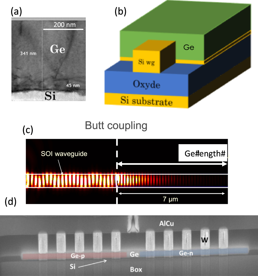
The well-known increase in the volume of digital communications, mainly driven by the generalization of cloud computing and mobile internet access, has as a consequence a strong increase in the traffic within the datacenters all over the world [51]. This growth is expected to continue to double every three years until 2020, and may further increase with the rise of the so-called 'Internet of Things' (IoT). As a consequence, the number and reach of optical links inside the datacenters is continuously increasing. At the same time, link price, performance and power consumption need to improve in order to decrease the technology cost ($) and the energy cost (pJ/bit) of data transmission. The main way to achieve such an improvement is to increase the integration density of the photonic components. Re-using the standard of Si-manufacturing technology used for 60 years by the electronic industry has been proposed and thoroughly studied since the early 2000s. After 15 years of research, SOI-based silicon photonics products are now emerging. This is the result of the intensive demonstration of basic building blocks allowing transport, modulation and detection of telecom wavelengths (1.3–1.55 μm) on Si wafer. On the one hand, despite all of this progress, current-integrated Si-photonics (see, for example, figure 10) is still only a 'challenger' of the well-established discrete-component solution, mainly based on III–V (InP-based) process technologies. On the other hand, Si-photonics has strong potential in terms of evolution and use. This is the only technology able to achieve ultra-high-density (>10 Tb/s/cm2), paving the way for low-cost and energy-efficient chip-to-chip communication. This would potentially allow the replacement of current metallic interconnects, which are today a limiting factor for the evolution of CMOS technologies. Therefore, several advances in terms of integration and performance will be necessary in the coming years to impose the Si-photonics as the standard of the optical communication market on a wide range of reach (from cm to 10's of km).

Figure 10. Overview of current fully integrated silicon photonics technology using a 3D electronic integrated circuit (IC).
Download figure:
Standard image High-resolution imageCurrent and future challenges
Current silicon photonics technology is at a maturity level similar to the one of the electronics industry in the 1980s. Transition between discrete components and the integrated system is occurring, allowing us to respond to the need for cost-effective systems. In the Si-CMOS industry, performance improvement and new functionalities (application range) came from the scaling of dimensions. Since the performance improvement of photonics will not come from such a scaling (fundamentally limited by the optical wavelength), it has to come from the process integration possibilities. Complex integration solutions can be used to resolve some of the several challenges of silicon photonics. First, the integration of electronics and photonics needs to be compliant with the CMOS technology roadmap. If a monolithic integration of photonics into electronics has been demonstrated [52], this approach is not the most efficient in terms of overall effort with regard to advanced CMOS nodes (i.e. 55, 28, 20 nm, etc) for the electronic part. Solutions such as 3D or 2.5D integration [53] using a copper pillar allows for the separation of both electronic and photonic processes and opens the door to a fully dedicated process optimization for the photonics die. This solution is currently used to integrate the transimpedance amplifier (TIA) and modulator drivers [54, 55], but in the future an improved interconnect density will be needed in order to allow several chips (e.g. CPU and Memory) to communicate together. The second challenge is the optical performance of the individual components. For example, fully integrated Si-photonics is not yet able to perform the complex functions of high-end discrete-component-based circuits such as dense multiplexing/de-multiplexing, mainly due to the need for thermal control of the Si-based devices. Another example is the limitation of the device performance resulting from the trade-off between the available SOI wafer structure and processing (limited by initial SOI and buried oxide (BOX) thicknesses, the number of mask levels and the process dispersion) and the optimal design of the various components (e.g. waveguides, grating coupler, and modulator) that would usually require several different Si-thicknesses. Another widely discussed challenge of Si-photonics is the lack of a monolithically integrated light source. Without this stumbling block in the development of the technology, a full integration would allow the further reduction of the die-cost, and it would be mandatory for the future integration at the chip-to-chip level, where several compact sources would have to be used. Finally, a future challenge will be the diversification of the SOI-based Si-photonics technology in order to increase the return on investment of the significant development effort. Therefore, SOI-based Si-photonics should also be used for other purposes than interconnect applications.
Advances in science and technology to meet challenges
The evolution of Si-photonics in the next decade will require the implementation of several new process steps (see figure 11). From a front-end perspective, an efficient device optimization can be achieved by introducing multiple SOI patterning, allowing the co-integration of several structure types such as strip-waveguide and rib waveguide with various SOI thicknesses and slab thicknesses, and also better shape control. This will come with an improved control of the lithography (using for example 193 nm immersion lithography) and the development of optical proximity correction (OPC) compatible with non-Manhattan (rounded) shapes, but also with an improved control of the variation of the amount of etched Si by using, for example, gas cluster ion beam (GCIB) correction techniques. The substrate itself can be a source of improvement, when incorporating smart BOX structures such as photonic crystals in order to manage the coupling performance of the optical I/Os [56]. The second advance will be the integration of new material layers allowing us to mitigate the intrinsic weaknesses of Si, especially its thermal sensitivity of the optical index, poor electro-optic coefficients and indirect-band-gap. Recently, 'midex' materials (featuring optical index between ∼1.6 and ∼2.5) have attracted a lot of attention based on their thermal properties. Several demonstrations of low T° dependence passive devices using SiN [57], TiO2 or AlN have been made. Those materials are compatible with CMOS fabs and will now be integrated with Si-photonics platform, thus enabling low power dense wave division multiplexing (DWDM) solutions. An additional interesting feature of midex materials is their potentially higher Pockels coefficient, which may lead to the demonstration of electro-optical modulators. On the source side, the demonstration of III–V/Si hybrid laser has already been made [58] by taking advantage of the SiO2-SiO2 molecular bonding technique of InP dies over Si wafers. Still, the integration of such a hybrid laser into a complete Si-photonics transceiver will require innovative developments. Indeed, the laser stack thickness being comparable to a standard CMOS interconnect stack, the bonding method cannot be reused directly on a complex chip, and an innovative integration scheme based either on a backside laser integration, or local InP/InGaAs epitaxy over Si will be needed. A further step will be the integration of ultra-compact photonic-crystal-based hybrid nano-lasers [59] for ultra-short reach applications. From the interconnect perspective, the development of TSV and stitching lithography (allowing the fabrication of dies beyond the size imposed by lithography-stepper limitation) will enable the Si-photonics interposer technology, allowing for the first time the integration of complex electronics such as application-specific integrated circuits (ASICs) together with the driving electronics of the photonics, then later chip-to-chip communication between several CPUs. At last, diversification of Si-photonics will also rely on the possibility of material integration. Some bio-sensing techniques already use the possibility of integrating SiN waveguide or metallization to enable plasmonic devices on Si waveguides, but a wider range of sensing application could emerge by extending the photonics to the MIR range. Here, Ge-based photonics technology would have several advantages by allowing the fabrication of passive devices, SiGe-QW-based modulators and detectors [60] and even Ge lasers. This will necessitate advances in the monolithic integration of high-quality Ge layer on SOI wafer, in the design of the basic building blocks, and the demonstration of an efficient electrically pumped strained-Ge-based laser.

Figure 11. (top) Process integration roadmap versus photonic node (bottom) schematic example of a future Si-photonics fully integrated SoC.
Download figure:
Standard image High-resolution imageConcluding remarks
Silicon-photonics evolution will go through the implementation of added functionalities thanks to the integration of new processes and materials. Substrate functionalization, stacking of III–V layers, midex materials, or high-quality Ge layer on large size Si-photonics interposer are compatible with CMOS current and future processes. Thus, Si-photonics has a strong potential to evolve similarly to CMOS-based system-on-chip (SoC) by not only becoming a standard of optical the interconnect market, but to extend to other applications related to the development of IoT, such as sensors.
7. Packaging of silicon photonic devices
Peter O'Brien
Tyndall National Institute
Status
Silicon photonics offers the possibility of low-cost mass-producible photonic systems complete with integrated electronics using well-established CMOS wafer-processing techniques. However, the challenges associated with packaging silicon devices is often underestimated and can significantly impact on the performance and cost of the overall photonic module. Numerous processes have been proposed to package optical fibers, integrated sources and electronics and manage thermal effects. However, these processes cannot be used unless they can be implemented in a high-volume manufacturing environment, using automated packaging equipment based on fast and low-cost assembly techniques.
Current and future challenges
The main challenges associated with packaging silicon photonic devices include:
- 1.Packaging of single-mode fibers, especially fiber arrays, ensuring high coupling efficiency and a fast fiber-to-waveguide alignment process.
- 2.Integration of sources, including passive optical components such as micro-lenses and isolators.
- 3.Integration of control electronics such as drivers and amplifiers, and the efficient routing of high-frequency electrical transmission lines to and from these electronics components.
- 4.Management of thermal effects, especially through the use of efficient thermal designs and passive cooling techniques that avoid power-hungry thermo-electric controllers.
- 5.Development of packaging processes for all of the above using fast, automated and high-volume packaging equipment, similar to that commonly used for electronic device packaging.
We are now beginning to see these challenges being addressed and the solutions made available to a wide user base, often through MPW or open-access foundry services [61]. Importantly, these packaging solutions are being captured in process design kits (PDKs) or packaging design rules and implemented through software tools. Like device or chip design processes, design rules ensure packaging follows standards that will facilitate ease of implementation which will drive lower manufacturing costs. This review article will focus on three key areas of silicon photonic packaging; 1) Fiber coupling, 2) Electronic packaging, and 3) Packaging design rules.
Advances in science and technology to meet challenges
Fiber packaging
The main challenge associated with coupling light from an optical fiber to a silicon waveguide is the large mismatch between the mode sizes. In single-mode fiber, the mode field diameter (MFD) for 1550 nm light is approximately 10 μm, while the cross section of the corresponding strip silicon waveguide is usually just 220 × 450 nm. There are two approaches to fiber coupling, edge and grating coupling. Edge coupling is already an industry standard for fiber packaging of III–V devices [62]. Grating coupling diffractively couples light from a near-normally incident fiber-mode into the silicon waveguide [63]. Ultimately, the best fiber coupling solution for a given device is application- and cost-dependent. Fiber coupling mostly uses an active alignment process, where the optical power is continuously monitored during the fiber alignment procedure. This can result in a slow and costly process, not suitable for mass manufacture. For example, we have developed a planar-fiber-array coupling process that uses shunt waveguides to more quickly align the fiber core to grating, while maximizing the coupling efficiency [64], see figure 12. However, besides taking considerable time, the fiber array consumes a relatively large portion of the expensive CMOS chip area, principally due to the minimum pitch possible between adjacent fibers in the array (127 μm pitch for standard SMF fiber). Therefore, there now is a drive to introduce passive-alignment processes that also reduce the fiber pitch to values approaching 50 and 25 μm. There are recent examples of passive fiber alignment processes for both edge [65] and grating [64] coupled designs. Both can use automated vision systems, avoiding the need for continuous active power monitoring. Furthermore, these passive processes can be combined with waveguide 'interposers' which taper-down the fiber pitch from 127 to 25 μm, ensuring minimum CMOS chip area is used for the fiber interface, enabling smaller and more cost-effective chip sizes.

Figure 12. Planar fiber array packaged to a silicon photonic device using grating couplers. The inset shows the grating coupler array with two outer shunt waveguides to assist with the alignment process.
Download figure:
Standard image High-resolution imageElectronic packaging
The packaging of silicon photonic devices with electronic drivers, amplifiers and other control circuitry is becoming a significant challenge as demand grows for higher levels of photonic–electronic co-integration and operational frequencies (>25 GHz). Most designers adopt a hybrid integration approach, either through flip-chip of the electronic IC onto the photonic device (3D integration) or connecting them via an electronic interposer (2.5D integration). Hybrid integration allows for the separation of the CMOS fabrication processes, enabling a smaller and more expensive CMOS node size to be used for the electronic IC that is not necessary for the photonic device. An example of 3D integration is shown in figure 13, where an electronic IC is packaged directly on the silicon photonic device. Direct packaging minimizes electrical transmission lines, which reduces electrical power consumption and maximizes operational frequencies. The packaging process is based on a eutectic flip-chip technique which uses an array of 20 μm copper pillars capped with 5 μm AgSnCu solder. Challenges still to be overcome are the development of TSVs which avoid the use of wirebonds and facilitate the integration of the assembled photonic–electronic sub-system on a carrier substrate (e.g. AlN ceramic) which can support high-speed electrical transmission lines, while also dissipating heat generated by the sub-system. Finally, a large part of the packaging cost can be consumed by the electrical components, especially the high-frequency electrical connectors (e.g. V-, K- and SMP-type). These can be more costly than the optical components and take up more space in the package, which needs to be considered by designers.

Figure 13. Packaging of an electronic IC (driver) on a silicon photonic device using a eutectic flip-chip bonding process. The inset shows a cross section of a single copper pillar with a AgSnCu solder cap used to form the bond between the devices.
Download figure:
Standard image High-resolution imagePackaging design rules
A key factor which has determined the success of CMOS electronics has been the focus on design standards, avoiding highly customized and untested designs. Standardization enables a wide user base to avail itself of libraries of mature and reliable design elements which ultimately drives down cost. Silicon photonics offers a similar capability which makes it highly attractive for mass-market applications. However, packaging must be part of this effort to ensure it is not the weak link in the supply chain. Therefore, significant effort is now being placed on developing packaging standards based on standard design rules which ensure as many users as possible implement chip-level designs that can be more easily packaged. Factors including optical waveguide and electronic bondpad pitch, location of DC and RF connections on the chip and the use of shunt waveguides for alignment are fundamental but extremely useful design rules. An indication of success, as with electronics, is the implementation of these design rules or PDKs within software tools such as Mentor Graphics and Phoenix Software [66]. This ensures that designers can more easily realize chip-level designs that are compatible with foundry packaging services. Packaging standardization is expected to have a greater influence on photonic chip design in the coming years and will greatly accelerate the up-take and commercialization of silicon photonics.
Concluding remarks
The growing interest in silicon photonics is mainly driven by its ability to satisfy high-volume market applications. Although wafer-scale processing can meet this demand, packaging can be a device-by-device process which is difficult to scale. Packaging challenges remain in areas such as fiber array coupling, source and electronic integration and efficient thermal management. Overcoming these challenges not only needs more innovative designs, but increased collaboration with equipment suppliers to ensure that faster alignment systems can be developed using passive and automated packaging systems. This, along with the use of standard packaging design rules, is the best way forward to ensure that future market demands can be met.
8. Silicon photonics for mid-infrared application
Goran Z Mashanovich and M Nedeljkovic
University of Southampton
Status
MIR silicon or group-IV photonics has been attracting attention recently as Si and Ge are transparent up to approximately 8 and 15 μm, respectively, and offer a range of applications in biochemical and environmental sensing, medicine, astronomy and communications. The MIR covers a broad wavelength range whose definition varies depending on the research community. In this paper, we consider that it covers from 2 to 20 μm. This range contains absorption fingerprints of a number of molecules as well as two atmospheric transmission windows (3–5 and 8–14 μm). The most popular silicon photonic platform, that of SOI, can be used only up to 4 μm due to high absorption loss of silicon dioxide [67, 68], and therefore alternative material platforms have to be utilized for longer wavelengths [68]. In addition, to fully exploit the transparency range of SOI, 400 or 500 nm thicker overlayers need to be used rather than the most popular 220 nm platform. A number of SOI devices, such as low-loss waveguides, couplers, splitters, filters, interferometers and spectrometers have been demonstrated at a wavelength of 3.8 μm [69]. In the last few years, other material platforms have also been investigated: silicon-on-sapphire (SOS) [70], silicon-on-porous silicon, silicon-on-silicon nitride, suspended silicon [71] and germanium-on-silicon [72]. Non-linear effects have also been reported in SOI [73], SOS and Ge-on-Si [74]. MIR Si photonic active devices such as modulators and detectors have been fabricated [75] as well as III–V sources and detectors integrated on SOI platform at 2–2.5 μm [76]. MIR Si-photonics is a new research field which is significantly less developed than its NIR counterpart. There is also scarcity in characterization equipment compared to the NIR region. Therefore, there are fewer publications and significant research effort still needs to be carried out to fully realize the potential of this field.
Current and future challenges
The MIR covers a much larger wavelength range compared to the NIR and it is not possible to find a silicon-based material platform that is transparent in the entire range. Silicon dioxide has large absorption from 2.6 to 2.9 μm and beyond ∼4.0 μm [67, 68]. That means the SOI platform with well-established fabrication of high quality wafers can be used only in a part of the MIR. For wavelengths longer than 4 μm alternative platforms can be SOS and Si-on-Si3N4. However, not only are high-quality SOS and Si-on-Si3N4 wafers not readily available, but sapphire and silicon nitride are transparent up to ∼5 and ∼6.5 μm, respectively, again limiting the usefulness of the two platforms for longer wavelengths. If the BOX in SOI can be removed and replaced with air, such a platform would utilize the full transparency of silicon (up to 8.5 μm) [67]. There are several approaches to fabricate suspended Si devices, however each of them has certain disadvantages. Photonic crystals are obvious candidates, but the operational bandwidth is limited. Silicon-suspended waveguides can be obtained by using electrochemical etching and subsequent removal of porous Si. However, the fabrication is complex and it is also difficult to obtain small features. If holes are etched near a rib waveguide, such that they do not disturb the propagation of the optical mode, they can be used to etch silicon dioxide by HF and thus create an undercut waveguide. The fabrication process involves two dry etch steps (for the formation of the rib waveguide and holes) and one wet etch step. Due to the existence of the slab region, these waveguides can bend and could have issues with mechanical stability. Another method is to have only one dry etch step by forming subwavelength lateral gratings that serve both as lateral claddings and access points for SiO2 removal by HF [71] (figure 14). The waveguides based on this structure should be more mechanically stable, but its stability may be compromised for more complex devices such as couplers, splitters, filters, etc. Also, integration with active devices and electronics may be problematic for all suspended structures since there is no solid bottom cladding. The so-called 'fingerprint' region (8 μm < λ < 14 μm) is particularly interesting for sensing as unique absorption bands exist for many molecules in this region. The most promising group-IV candidate for this region is Ge as it is transparent up to 14–15 μm. Ge-on-Si platform (figure 15) has a stable bottom cladding and can have sub dB/cm losses in the MIR [72]. As Si becomes lossy for λ > 9 μm alternative solutions may be needed for longer wavelengths, although this loss increase might not be prohibitive if high confinement in the Ge core is achieved. The small refractive index contrast between Si and Ge increases photonic integrated circuit footprints compared to those based on silicon/SOI, while the high-index contrast with the air top cladding limits the evanescent mode that could interact with an analyte. Suspended Ge structure may again be a viable candidate for extension of the transparency range. If a solid bottom cladding is required, Ge on a glass (e.g. chalcogenides which are transparent to 16–20 μm) could be a good candidate, although bonding techniques need to be investigated in order to obtain a robust platform. Once a suitable material platform has been chosen, integration of photonic devices with electronics can be investigated, which is a formidable task.

Figure 14. Suspended Si platform.
Download figure:
Standard image High-resolution image
Figure 15. Ge-on-Si MIR platform.
Download figure:
Standard image High-resolution image
Advances in science and technology to meet challenges
Integrated, compact, low-cost and low-energy MIR group-IV sensors will have significant advantages over the expensive and bulky solutions currently used. Such devices could be used as breath analyzers in disease diagnostics, for environmental monitoring, or for toxic and explosive sensing. To address the 'explosion' of internet traffic, low-loss optical fibers, and fiber sources and amplifiers in the 2–3 μm range are being actively researched to increase the current capacity. Low-cost and low-energy group-IV integrated circuits that would comprise both active and passive photonic components may find application in nodes of such networks. These examples stress the importance of the development of MIR silicon photonic devices and integrated circuits. For the latter application, SOI platform is probably the most suitable due to the maturity of fabrication processes and availability of high-quality wafers. Depletion modulators should be effective at these wavelengths, and graphene modulators can also offer high speeds with low power consumption and relatively small footprint. For on-chip sources, integration of III–V lasers on SOI platform, similar to the NIR solutions, is probably the most straightforward approach in the 2–2.5 μm range. For high-volume manufacturing in a foundry, monolithic group-IV photonic integrated circuits would be the most desirable approach. There is intensive research activity on GeSn MIR sources and recently an optically pumped GeSn laser has been reported [77]. The next main challenge is to demonstrate an electrically pumped GeSn/GeSnSi laser. For detectors in this wavelength range, candidates are bonded III–V detectors [76], GeSn-based detectors, graphene, and defect-engineered Si detectors. Although Si is transparent beyond 1.1 μm, it can be used as a photodetector if mid-bandgap states are created by ion implantation. Such photodetectors are CMOS compatible and easy to fabricate. An SOI p-i-n photodiode implanted with boron that operated at a wavelength of 2 μm with a speed of >20 Gb/s has been recently demonstrated [75]. Further optimization is required to increase the responsivity and decrease the bias voltage. The fingerprint region imposes more serious challenges in terms of active devices and their integration with passive MIR photonic circuits. The most likely optical modulation mechanism in Si and Ge will be absorption. Quantum cascade lasers (QCLs) that cover this wavelength range have been developed, but their integration with a Ge photonic platform that is transparent in this range, may prove quite challenging. QCLs are power-hungry devices that require complex fabrication of multiple layer stacks and they are thick compared to Ge photonic circuits. The integration of efficient detectors in this wavelength range may be even more challenging as there are not many options. Graphene is a promising candidate as it should have high absorption in the fingerprint region. Microbolometers are another option. Non-linear effects [76] can also be employed to upconvert the signal to shorter wavelengths where efficient detectors exist.
Concluding remarks
MIR silicon photonics is a relatively new research field. The MIR covers a large wavelength range and there is currently no material platform that can be used through the entire range. For particular applications and chosen platforms, development of both passive and active devices, improvement of their performance and integration on a chip will be the main challenges in the near future. The fabrication of integrated photonic circuits for the fingerprint region is particularly challenging as there are not many options for sources and photodetectors in this wavelength range.
Acknowledgments
Funding from the EPSRC and the Royal Society in the UK (MIGRATION, Silicon Photonics for Future Systems, and CORNERSTONE projects, and Goran Mashanovich's Royal Society Research Fellowship) has supported this work.