

Abstract
High-speed optical interconnects are crucial for both data centers and high performance computing systems. High power consumption and limited device bandwidth have hindered the move to higher optical transmission speeds. Integrated optical transceivers in silicon photonics (SiP) using pulse-amplitude modulation (PAM) are a promising solution to increase data rates. In this paper, we review recent progress in SiP for PAM transmissions. We focus on materials and technologies available CMOS-compatible photonics processes. Performance metrics of SiP modulators and crucial considerations for high-speed PAM transmissions are discussed. Various driving strategies to achieve optical PAM signals are presented. Some of the state-of-the-art SiP PAM modulators and integrated transmitters are reviewed.
Export citation and abstract BibTeX RIS
1. Introduction
Multi-level pulse-amplitude modulation (PAM) provides an economically viable approach to higher data rates with affordable cost and complexity. Conventional non-return-to-zero (NRZ) modulation cannot support higher data rates required in the next generations of optical links in data centers. This is simply due to the fact that the analog bandwidth of optical and electrical components cannot keep pace with the growth in data traffic. Increasing the number of fibers (e.g. achieving 25 Gb s−1 400 Gb s−1 via VCSELs by 16 separate multi-mode fibers) could meet demand, but is not economically viable. For reach greater than a few hundred meters, single-mode fibers are used, but fiber costs go up. Higher-order modulation formats, such as quadrature amplitude modulation, and coherent detection can effectively increase single-channel data rates within a given analog bandwidth, and are exploited in commercial, long-haul transmission systems. However, coherent detection is expensive and requires complex optical and electronic components, such as local oscillator and fast digital signal processors (DSP).
Optical interconnects for applications such as data centers and high performance computing (HPC) require high data rates, but also have very stringent requirements on cost and energy consumption. PAM provides a good compromise between data rate and complexity. PAM allows for direct direction of optical intensity signals without requiring complex DSP, although good signal-to-noise ratio (SNR) is required. The IEEE 400 Gb s−1 Ethernet task force (IEEE 802.3bs) has converged on 4-level PAM (PAM-4) for links from 500 m to 10 km [1]. This can be realized using 50 Gb s−1 by 8 wavelengths or 100 Gb s−1 by 4 wavelengths in a grid of coarse wavelength division multiplexing or local area network (LAN) WDM. Future terabit links may require higher-order PAM and a finer WDM grid for higher spectral efficiency and transmission capacity.
Silicon photonics (SiP) has quickly emerged as an enabling technology for large-scale integrated photonic circuits [2, 3]. Capable of manipulating electrons and photons on the same platform, SiP promises to pack more functionality on a single chip [4]. It uses the advanced manufacturing process of microprocessors, known as the CMOS process, by which tens of billions of transistors have been integrated on a single chip. This disruptive technology is based on high-index-contrast materials allowing for extremely strong optical confinement on the nanometer-scale, leading to orders-of-magnitude reduction in footprint and cost. Optical interconnects are the major commercial application of SiP. They are driven by the quickly increasing demand for high-speed optical links in data centers [5].
Optical modulation is an essential function in an optical link. Since the first GHz demonstration [6], silicon optical modulators have attracted tremendous interest [7]. SiP foundries are now widely accessible to academic researchers and small industry groups. This has considerably accelerated the research and development of SiP modulators in the last few years. Various devices and driving strategies have been examined for optical PAM signal generation on silicon. Significant effort has led to record-breaking demonstrations of single-channel data rates beyond 100 Gb s−1 and ultra-low energy consumption down to 1 fJ/bit. Substantial progress in CMOS-photonics co-design and integration has been made towards fully integrated CMOS-driven optical PAM transmitters.
Here, we review recent progress on silicon photonic modulators and transmitters for PAM transmissions. While there have been significant progress and impressive demonstrations using new materials and hybrid structures, we will focus on materials (doped silicon and germanium) and technologies available in generic wafer-scale CMOS-compatible photonics processes. The rest of this paper is organized as follows. We first discuss the figures of merit (FOM) of modulators and considerations on optimizing silicon photonic modulators for PAM transmission (section 2). In section 3, we review driving strategies to achieve optical PAM signals. Section 4 reviews some of the sate-of-the-art devices, including modulators and CMOS-photonic PAM transmitters. In section 5, we discuss the challenges and opportunities for future terabit optical links.
2. Performance and FOM
In this section, we discuss performance metrics of SiP modulators and crucial considerations for high-speed PAM transmissions. The section is organized as follows. To facilitate our discussion, we first briefly review fundamentals of silicon electro-optical phase shifters, including the phase modulation mechanisms and commonly used phase shifter structures. Then we discuss, in the context of a PAM transmission link, the power penalties induced by a SiP modulator due to its limited efficiency, insertion loss and limited bandwidth. Based on the transmission link penalty, we discuss conventional FOM of optical modulators and present a new FOM proposed for SiP PAM modulators. Afterwards, we review other important characteristics that need to be considered in designing a PAM link using SiP modulators, such as energy consumption, chirp, linearity, and timing impairments. At the end of this section, we discuss DSP options for PAM transmissions.
2.1. Silicon electro-optical phase shifters
2.1.1. Phase modulation in silicon
Since the linear electro-optical effect (Pockels effect) is absent in unstrained silicon, the plasma dispersion effect is the most commonly used to achieved phase modulation in silicon [8]. Using the Drude model [9], the change of refractive index ΔnSi and the excess loss  due to the free-carrier absorption are functions of density variations in free electrons and holes (Δn and Δp) and are given by

where the wavelength (λ0) is given in meters, the carrier densities per cubic centimeter, and the change in absorption per centimeter

Using the plasma dispersion effect, various modulation mechanisms (such as carrier accumulation, carrier injection, and carrier depletion) and their implementation structures (namely, phase shifters) have been examined [7]. In all the mechanisms, the essential idea is to vary the silicon waveguide's effective index by changing the free-carrier distributions. The phase modulation is proportional to the change of the effective index Δneff as function of the applied voltage V, which can be calculated performing the mode overlap between the optical field ( ) and the free-carrier distributions:

The term dneff/dnSi describes the dependence of the effective index neff on the material index nSi and is very close to one. Here, we define x and y to be the vertical and lateral direction, respectively, and z the longitudinal direction of the waveguide. Note that the free-carrer absorption is modulated in the same time.

Clearly, increasing the carrier densities and their overlap with the optical field leads to a higher modulation efficiency but also causes higher absorption. The design of a silicon phase shifter is a compromise between efficiency and loss. The carrier transport dynamics (present as RC elements in the circuit level) also needs to be considered as it limits the modulation speed. These tradeoffs will be further discussed in the following subsection in examining the modulator FOM.
Figure 1 shows cross-sectional schematics of three phase-shifter structures the most explored for SiP PAM modulators. The first applies the mechanism of carrier depletion. It uses a lateral pn-junction embedded in a rib waveguide (figure 1(a)). The diode works under reverse bias where the width of depletion region changes as function of the voltage across the diode. Since there exists no free-carrier in the depletion region, the effective index of the waveguide also changes as the voltage.
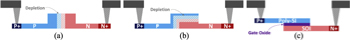
Figure 1. Cross-sections of silicon phase shifters using (a) lateral pn-junction, (b) vertical pn-junction and (c) SISCAP.
Download figure:
Standard image High-resolution imageThe second structure also works in the depletion-mode but uses a vertical pn-junction (figure 1(b)) where the optical mode overlaps with the depletion region along the lateral direction. Because the waveguide is typically designed to have a width (e.g. 500 nm) larger than than the height (e.g. 220 nm), the vertical junction has a larger depletion region overlapped with the optical mode and thus a better modulation efficiency. However, for the same reason, it also has a higher abortion and a bigger junction capacitance that limits the operating bandwidth.
The third structure is based on a silicon-insulator-silicon capacitor (SISCAP) structure [10] with a very thin oxide layer (typically 5–10 nm) between a SOI layer in the bottom and a poly-Si on the top. The accumulated charges (free carriers) on the top and bottom of the oxide capacitor are changed by the applied voltage for phase modulation. Due to the better mode overlap and higher free-carrier densities, the modulation efficiency of SISCAP is an order-of-magnitude higher than that of the depletion-mode phase shifter using a lateral pn-junction, but also has a significantly higher absorption loss and capacitance.
2.2. Figure of merit of MZM design: efficiency, loss, and bandwidth
Consider the normalized transfer function of a typical Mach–Zehnder modulator (MZM) in figure 2. Several impairments affecting PAM performance can be identified in the transfer function. First, the optical loss degrades the transfer function extrema, i.e. a reduction in overall extinction ratio (ER). The voltage Vπ is defined as the voltage swing to go from maximum to minimum output. To avoid nonlinearities of the modulator transfer function, the RF input voltage (Vin) is scaled to a peak-to-peak voltage falling in the linear region of the MZM response, i.e. smaller than Vπ. We refer to this affect as modulation loss, which is determined by the operating point, i.e. the input voltage excursion vis-a-vis Vπ.
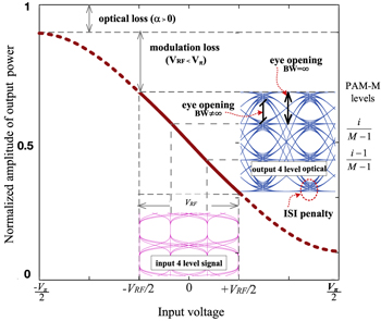
Figure 2. Typical optical power transmission (normalized) of a SiP MZM. The insets show the noiseless eye diagrams for PAM-4 modulation format with gaussian shaped pulses with BWEO/BR = 0.9.
Download figure:
Standard image High-resolution imageThe lower inset in figure 2 (in pink) is a typical electrical multi-level eye diagram, in this example PAM-4. The output eye is given in the second, upper inset (in blue). Were there no bandwidth limitations (electrical or electro-optic (EO)), the eye opening would span the entire distance between rails in the eye diagram. Limited bandwidth leads to a more closed eye, which we refer to as the intersymbol interference (ISI) penalty. Instead of achieving one of the four levels at the sampling time, limited bandwidth smears the levels, leading to ISI.
2.2.1. Efficiency-loss as a FOM
Conventional modulators (such as LiNiO3) have low loss and, due to the linear EO effect, the effective index change is linear in applied voltage. This leads to a linear relationship between phase and applied voltage, since

The linearity of Δneff in applied voltage also leads to a linear relationship between Vπ and L. The conventional FOM developed for non-SiP modulators takes the form of phase modulation efficiency, i.e. the product Vπ L. It has also been widely used in demonstration of silicon modulators.
However, SiP solutions have high loss and typically use the plasma dispersion effect [8] to manipulate phase due to the lack of the linear EO effect. The Δneff is nonlinear in applied voltage, making the phase change (5) nonlinear in applied voltage, and also making Vπ nonlinear in L. Another FOM for SiP introduced a loss factor, α to the efficiency, leading to VπαL (typically given in dB V) that has been adopted for the optimization of silicon phase shifters [11, 12].
However, changes in L lead to complex behavior in Vπ and BW that cannot be captured by the efficiency-loss product. The efficiency-loss FOM is particularly inappropriate for PAM as it neglects the bandwidth effects that lead to ISI.
2.2.2. FOM for PAM
SiP modulators should be designed to have good ER and wide bandwidth. However, these goals may be conflicting, especially in the design of a traveling wave, MZM configuration. The modulator bandwidth, BW, and Vπ are determined by the phase-sifter length, L for a given fabrication process. This single parameter L, therefore, affects the three types of impairments for PAM modulation that we see in figure 2. The optical loss is determined directly by L: the longer the phase shifter, the more optical loss incurred. Modulation loss is determined by the relationship between Vπ and L; this relationship is nonlinear due to the nonlinear variation of effective index of refraction with applied voltage. Finally, the ISI penalty is determined by the relationship between BW and L, yet another nonlinear relationship.
Given a certain context of device-level design—a certain fabrication process, reference modulator design, RF and optical velocity matching, etc—we would like to find the optimal value of L. Rather than using ER and bandwidth alone as quality indicators, we would ideally include system-level design choices such as modulation format, baud rate, driving strategy (linear region, CMOS drivers, low-power), etc. A good FOM would inform your design choice using both device-level and system-level parameters.
In [13, 14], we propose a FOM to capture the bandwidth impairments as well as efficiency and loss. The first step is to find the modulator power penalty (MPP) or modulator-induced transmitter power penalty (TPP) that includes losses from ER, PAM multi-level modulation, and ISI due to limited bandwidth. In figure 3, we present a simple numerical model for the modulator. The bandwidth constraint is modeled by a linear filter with impulse response having a Gaussian shape parameterized with the modulator 3 dB bandwidth BW. A square wave data signal with average power Pin at baud rate BR with PAM modulation level M is bandwidth-limited by this filter. The electrical filter output goes through an instantaneous nonlinearity defined by (5) to determine the final optical output signal with power Pout(t). We see in figure 3 how Pout is found numerically, and how the MPP is related to contributing loss (material loss, ER and ISI).
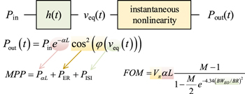
Figure 3. Numerical model for SiP modulator used to derive modulator power penalty (MPP) and figure of merit (FOM).
Download figure:
Standard image High-resolution imageWe next found a normalized version of the optical modulation amplitude, defined in the following, that is closely correlated with MPP from our model
where 'open eye' refers to one of the output PAM eyes illustrated in figure 2. When OMAN is maximized, MPP is minimized. From the OMAN, we developed the following FOM for PAM (FPAM)

2.2.3. FOM performance
This new FOM is a simple closed form expression of easily identified and/or measured quantities. The ratio of bandwidth to baud rate in the FOM captures the contribution to ISI, while the αVπL captures the efficiency. The FOM is adapted particularly to PAM modulation as captured by the M term in the FOM. This bandwidth-aware FOM has been validated by Monte Carlo simulations to be an effective predictor of optimal L. Thus optimal modulators can be designed for a given system target (modulation level M and baud rate BR). This FOM can also be used to sweep system parameters to predict penalty for a given modulator design.
For the purpose of illustration, we consider an MZM using the lateral pn-junction phase shifter developed on a general-purpose SiP platform [14]. In figure 4 we have plotted the modulator length L in mm versus both MPP (dotted lines) in dB and the FOM (solid lines). We vary the baud rate from 14 to 56 Gbaud and observe a bowl shape for all plots. At small L, the bandwidth is high and so the ISI penalty is small; the ER is small so the ER penalty is high. At high L, the bandwidth decreases making the ISI penalty large, while ER is high. The minimum finds a balance of these two contributions for an optimal choice of modulator length L. The stars show optimal L using the FOM, while diamonds give the true optimum L using the MPP. We can see in figure 4 that at low L, the two minima for dotted and solid curves coincide. At high L, the minima are different, however the bowl is very shallow, so the MPP associated with the minima are almost equal. Hence our FOM is a good predictor of an L that achieves minimum MPP. We have swept baud rate and reverse bias voltage and found that the MPP achieved using the FOM choice of optimal L never incurs more than 0.1 dB excess MPP [14].

Figure 4. FOM performance of a SiP MZM in lateral pn-junction: modulator length L in mm versus modulator power penalty (MPP, dotted lines) in dB (left axis) and FOM (solid lines) in the right axis for three baud rates.
Download figure:
Standard image High-resolution image2.3. Energy consumption
The energy consumption per unit bit is a crucial performance metric for assessing an optical link. The energy consumption of a modulator can be evaluated in different ways depending on how it is driven. Here we discuss calculation of the dynamic energy consumption for two types of modulation elements: one applies to TW electrodes (e.g. TW-MZMs) and the other to lumped driving elements (e.g. MRM and lumped phase shifters in an MZM). Note that this is only the RF power consumed by the modulator; more power may be consumed by DC elements (e.g. modulator biasing and thermal tuning of the center wavelength) and electrical amplifier circuits.
For a depletion-mode modulator using traveling-wave electrodes (e.g. a single TW-MZM or a phase-shifter segment applying a TW electrode in the BWS driving scheme), given the assumption that the RF transmission line (a microwave waveguide formed by the TW electrodes loaded by the pn-junctions) is impedance matched to the source and termination, the dynamic power consumed on high-speed modulation can be estimated by [15, 16]

where Vrmsis the root mean square (rms) voltage and Z0 the characteristic impedance of the transmission line. Then the energy consumed per bit Eb is given by

where b is the bit rate. Considering the impedance is typically around 50 Ohms, the power consumption is mainly dependent on the driving voltage of the TW-MZM. For a given baud rate, the energy per bit of a TW-MZM decreases with the PAM order.
For a depletion-mode modulator with a lumped driving electrode (e.g. MRM), the modulation power is dissipated inside the modulator on rising transitions, charging the capacitor, of capacitance C, in the depletion region of the p–n junction. In this case, the energy consumed by a rising transition of magnitude V is given by E = CV2. The total energy consumed ET by all rising transitions is given by [17]

where levels in a given PAM signal are assumed to be equally distributed across Vp−p, and M is the PAM order. Since there are M2 possible transitions in a PAM signal and  bit(s) per symbol, so the energy consumed per bit Eb is given by
Thus for a given driving voltage, the modulation energy efficiency will increase with the PAM order. Meanwhile, since the power consumption on thermal tuning is independent of the modulation speed, the total energy per bit will also decrease with increasing of baud rate.
Equations (8)–(11) are for a single modulation element. In the case where more than one modulation elements in a modulator, the total power consumption are simply their summation.
2.4. Linearity
Linear amplitude response is desired to achieve equally spaced eyes in PAM signal since the BER is limited by the least-open eye. The linearity of a modulator is characterized by the spurious-free dynamic range (SFDR). It is tested using two closely spaced frequency tones as inputs (here defined as f1 and f2) and measuring the linear outputs (at f1 and f2) and nonlinear response due to the harmonic distortions (e.g. second-order at 2f1 and 2f2) and intermodulation distortions (IMDs) (second-order at  and
and  third-order at
  ). SFDR is then defined by the ratio of the linear response to the nonlinear response at the input power when the nonlinear response reaches the noise floor of a 1 Hz bandwidth. SFDR is an important parameter for analog applications such as radio-over-fiber and microwave photonics; more details can be found in [18, 19].
Despite the inherent nonlinear phase and absorption responses in the plasma dispersion effect, SiP MZMs showed good linearity [20–22]. Up to 88.9 dB Hz1/2 of second-order SFDR and 113.3 dB Hz2/3 of third-order IMD-SFDR were measured using a SiP MZM [22]. Although still inferior to that of the best reported with a LiNO3 modulator (up to 121 dB Hz2/3 [23]), the linearity of SiP MZMs can well support higher-order PAM transmissions.
In contrast, MRMs showed a poor SFDR due to the second-order harmonic distortion (SHD) [24]. Ayazi et al measured a SHD-SFDR of 64.5 dB Hz1/2 and an IMD-SFDR of 84 dB Hz2/3 of an MRM and concluded that the most significant contribution of nonlinearity is from the pn junction rather than nonlinear transfer function of the resonator [25]. In [17], in order to achieve equally spaced optical eye in a high-speed PAM MRM, the electrical driving signal was pre-distorted with the extent depending on the bias and frequency detuning. The linearity of MRMs can be improved by using a structure of ring-assisted MZ interferometer (RA-MZI) where each arm of an MZI is coupled to an MRM operating in push-pull [26, 27]. A high SFDR of 106 dB Hz2/3 was measured in an RA-MZI modulator [27]. Recently, Shoman et al showed another interesting design that uses a thermal MZI switch in the coupler of an MRM to tune the ER as well as the linearity; equally spaced optical eyes were achieved without distorting the driving signal [28]. However, both cases require an additional wavelength-tuning mechanism that is not trivial given that the power consumption on wavelength tuning already dominates over optical modulation in MRM [17].
2.5. Chirp
Chirp is in general less concerned in short-reach links compared to long-haul communications. MZMs in push-pull operation generally have very low chirp. MRMs have a stronger chirp that can also be suppressed by using the RA-MZI structure [29, 30]. Nevertheless, the results in [17] showed that chirp in a single MRM was not a significant contributor to the signal degradation for up to 40 Gbaud PAM-4 over 5 km SSMF transmission. The simulation showed that for O-band transmission in a standard single-mode fiber around 1310 nm where the chromatic dispersion is zero, the nonlinear distortion in PAM signal due to modulator chirp has a negligible impact on the system performance for up to 2 km [31]. Up to 20 km 112 Gb s−1 transmission of PAM-4 using an O-band SiP modulator has been achieved without dispersion compensation [32]. However, C-band PAM transmission suffers from strong chromatic dispersion of SSMF that makes it difficult to achieve a baud rate beyond 40 Gbaud without dispersion compensation for a link longer than 2 km [33].
2.6. Timing impairments
In addition to the compression of eye opening due to the previously discussed imperfections (due to insertion loss, voltage-limited ER, and limited BW), eye diagram skew may also cause power penalties and increase the DSP burden. Skew makes determination of the optimum sampling point ambiguous, as it varies from eye to eye. The eye skew is becoming a crucial issue for VCSELs [34]. There is little research into the origin of eye skew in SiP modulators; for SiP MZMs eye skew is much less significant than it is for VCSELs. However, obvious eye skew has been observed in resonator-based SiP modulators [17] and GeSi EAMs [35] due to the high nonlinearity in their transfer function and EO response (see figures 11(c) and 12(c)). In segmented MZMs or cascaded architectures using compact MRMs (e.g. DAC-less driving configurations to be discussed in the next section), the skew will be exacerbated in the presence of delay mismatch between their driving signals [36, 37]. Eye skew will become more important as we push to higher baud rates as shorter rise/fall edges demand more accurate sample timing.
2.7. DSP options
DSP can significantly increase the baud rate and the transmission distance of an optical link. An important step in designing any system is to find the right balance of complexity and performance. For instance, both pre-compensation (transmitter side or TX) and post-compensation (receiver side or RX) algorithms have been widely examined for silicon photonic PAM transmitters. Bandwidth limitations in particular can be overcome by pulse shaping in the transmitter side and equalization in the receiver side.
Consider transmitter side pre-compensation options in DSP. Nyquist pulse shaping maximizes baud rate for a given bandwidth, but can significantly expand the signal time duration and introduce overshoots that limit modulation depth and increases quantization noise. Raised cosine shaping offers a way to trade-off spectral efficiency and robustness. Transfer function nonlinearity in the modulator can be reduced by DSP at the transmitter by digitally applying an inverse of the transfer function. Both pulse shaping and nonlinear correction at the transmitter require a high speed digital-to-analog converter (DAC) whose expense may not be appropriate for certain applications.
Even when a transmitter-side DAC is not warranted, several possibilities exist for receiver-side equalization that simply adds to the existing DSP chain without requiring additional hardware. Application specific integrated circuits (ASICs) for DSP might be larger with equalization, but that is only a small increase in complexity. Techniques such as minimum mean squared error (MMSE), zero forcing, or decision feedback equalizers can compensate for limited transmitter bandwidth. MMSE is the most common equalizer in recent articles on high speed PAM, requiring a training sequence followed by a decision directed mode. Equalization is used in addition to other typical DSP, such as timing recovery and forward error correction (FEC).
The use of FEC is a level of digital signal processing that may be appropriate in some settings. ASICs for DSP have space and power consumption dominated by modules for dispersion compensation and FEC. For short links, where PAM modulation is most likely to be employed, chromatic dispersion is negligible and FEC dominates ASIC complexity [38, 39]. The FEC complexity depends on the decoding technology used; higher performance decoding is iterative.
Two factors other than complexity weigh-in on the use of FEC: latency and spectral efficiency. All FEC decoders introduce latency, and iterative decoders multiply that latency by the number of iterations. Finally, two popular coding overhead choices are 7% and 20% overhead. The percentage represents the additional parity bits that must be transmitted, reducing the net throughput. Forward error correcting codes are only effective for a certain minimal quality of uncoded transmission, often referred to as the FEC threshold. The higher the overhead, the more we can tolerate a higher uncoded bit error rate. Typically we use 3.8 × 10⁻³ as the minimum uncoded bit error rate when using 7% overhead FEC, and 2.4 × 10⁻² when using 20% overhead FEC [40].
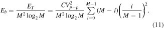
3. Driving strategies for PAM
3.1. Mach–Zehnder modulator
For generation of optical PAM signals, the conventional method is to generate the multi-level signals in the electrical domain. These signals can be transferred to an optical carrier using a DAC, an RF power combiner or an arbitrary waveform generator (AWG), as illustrated in figure 5(a). Due to the relatively weak phase response (the plasma effect [8]) in silicon modulator, we usually see long EO phase shifters with RF travailing-wave (TW) electrodes to achieve sufficient modulation depth. This design simplifies the interconnections between the modulator and its driver circuits and allows for their independent design and optimization. The use of a DAC has the added benefit of enabling pre-compensation in the digital domain as discussed in the previous section. Although convenient and flexible, a high-speed DAC is expensive and a significant source of power consumption. In contrast to the case of long-haul transmissions, the advantages of applying digital pre-compensation in short-reach links currently may not override the excess cost and increased power budget.
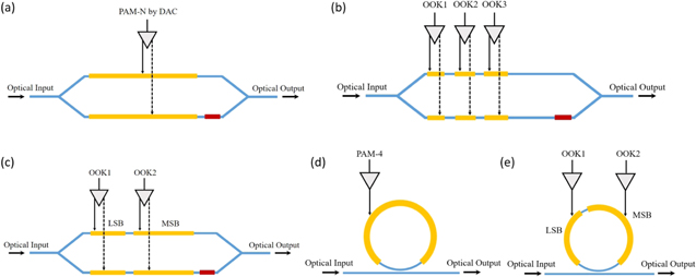
Figure 5. Schematic of PAM-4 using the (a) MZM transmitter using an electric DAC; (b) thermometer-coded segmented (UWS) MZM transmitter; (c) BWS MZM transmitter; (d) MRM transmitter using electric DAC; and (e) segmented MRM transmitter. Higher-order PAM formats can be achieved using similar configurations, e.g. using three segments in the BWS MZM for PAM-8.
Download figure:
Standard image High-resolution imageTo eliminate the cost of an electrical DAC and lower the system complexity, the use of a segmented MZM was proposed as early as 1980 [41] to act as an optical DAC. The MZM is segmented in a multi-electrode structure and each electrode receives an individual on–off keying (OOK) data stream, as shown schematically in figures 5(b) and (c). Besides being compact and power efficient, the segmentation of the MZM electrodes can assist in the trade-off between the electro-optical bandwidth and modulation efficiency [42]. In the conventional TW modulator, the length of the phase shifter limits the bandwidth, due to RF losses alongside the TW electrode and the velocity mismatch between the electrical and optical signals. However, in the segmented modulator, the driving signals are applied sequentially to the segments with precisely tunable timing circuits to match the optical signal delay between different segments. As a result, the interaction length can be increased, and the driving voltage lowered.
There are two segmentation topologies: unary-weighted segmentation (also called thermometer-coded segmentation [43]) and binary weighted segmentation (BWS). The thermometer code is implemented by employing a segmented MZM with segments of equal length (figure 5(b)). This approach has the advantages of identical segments, which simplifies the design of a phase-shift and driver unit. Each segment can be very short and thus be treated as a lumped element in the driving circuit. A number of low-power, distributed amplifiers can then be used to drive a long segmented optical phase shifter [44]. The delay between the amplifiers can be synchronized using TW transmission lines [45] and digitally controlled delay blocks [36].
The other segmentation approach uses weighted binary codes to determine the length of each segment, as illustrated in figure 5(c). In such a scheme, binary inputs can be directly applied to the RF drivers for a minimized number of segments, simplifying the driving configuration. A concern using BWS is the varied electrical characteristics of different segments. In particular, the bandwidth is typically limited by the segment for the most significant bit (MSB), as it is longest. The binary coding can also be applied to an uniform segmentation design, where a number of segments can be grouped to receive the same bit stream. In this case, the weight of each segment group is simply determined by the number of segments. Despite the excess complexity in electrical connections and delay control, both segmentation topologies help lower voltage swings, allowing for the use of low-power CMOS driver circuits [46].
Despite the advantages of an optical DAC, it was not until in 2008 that segmented transmitters garnered attention [47]. Recently interest has been reignited in exploiting segmented MZM in high-capacity short reach data links using silicon photonic transmitters [48]. PAM-4 transmission at 20 Gb s−1 used a segmented MZM with a silicon-insulator-silicon capacitive (SISCAP) junction [49]. Later, 128 Gb s−1 PAM-4 [50] and 114 Gb s−1 PAM-8 [51] were demonstrated using the p–n junction in carrier depletion.
3.2. Microring modulators (MRMs)
In addition to MZMs, MRMs [52–58] are another popular solution widely examined for integrated optical transmitters. They combine many desirable features, such as ultra-low-power consumption and unbeatable compactness. MRMs provide a scalable solution for optical interconnects and are attractive for high bandwidth-density chip-level communications [59]. However, MRMs are very sensitive to fabrication variations and temperature changes, so they require heaters and feedback controllers to lock the resonant wavelength [60].
Similar to an MZM, an MRM can be directly driven by a multi-level electrical signal generated using a DAC, as shown in figure 5(d). In this case, a phase shifter is inserted in the ring cavity for intra-cavity modulation. The output amplitude depends on the round-trip phase of the cavity. Due to the strong optical field built up in the cavity near the resonant wavelength, the modulation efficiency can be significantly enhanced compared to MZM. One or a pair of MRMs can be inserted in the MZI arms for a compact MZM, namely, an RA-MZI modulator that offers better linearity and chirp performance compared to single MRMs, as discussed in sections 2.4 and 2.5. Segmented phase shifters an also be used for DAC-less operation in MRM. Figure 5(e) shows an example, where the two phase shifter segments with different lengths (one for the MSB and the other LSB) are driven by two separate OOK drivers. Amplitude modulation of an MRM can also be achieved by modulating the coupling between the microring cavity and the bus waveguide. For example, in [61], a segmented MZM was used as a variable coupler of a microring resonator for DAC-less coupling modulation.
Another advantage of an MRM is that it selectively modulates a single WDM channel, enabling a multi-channel WDM transmitter without requiring an extra wavelength multiplexer [62, 63]. Using a multi-wavelength laser and cascaded MRMs coupled to a single bus waveguide [64, 65], an ultra-compact WDM transmitter can be realized. The resonant wavelength of each MRM can be tuned to the desired laser wavelength, with little impact on other channels. Combining this MRM-based WDM architecture with high-speed single-channel PAM operation can realize high-capacity integrated transmitters. Recently, real-time 200 Gb s−1 (4 × 56.25 Gb s−1) PAM-4 transmission over 80 km SSMF using a quantum-dot comb laser and silicon MRMs was realized [66].
3.3. Driving topologies using binary amplitude modulators (AMs)
In the driving architectures discussed previously, the optical PAM signal is achieved, in general, through phase modulation and optical interference or resonance. An optical PAM signal can also be achieved by combining a number of binary AMs. Figure 6 shows two architectures for PAM-4. The first is composed of two AMs arranged in series and driven by two separate NRZ drivers. The other is composed of two AMs arranged in parallel. An AM in these topologies can be an MZM, an MRM [37] and an electro-absorption modulator (EAM) [67].
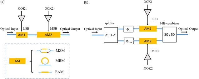
Figure 6. Schematic of PAM-4 in (a) AMs in series; (b) AMs in parallel. These topologies work for various kinds of AM such as MZM, MRM and EAM.
Download figure:
Standard image High-resolution imageIn the series architecture, figure 6(a), the response of the PAM modulator is taken as the product of the transfer function of each AM. Each AM produces a different OMA: one acts as MSB and the other as LSB. Although straightforward, this output suffers from the insertion loss of each AM.
In the parallel architecture, figure 6(b), the response of the PAM modulator is the vector addition of the transfer function of each AM. It consists of a power splitter, two identical EAMs, a DC phase shifter and a 3 dB combiner. By tuning the power splitting ratio between the two branches, one of the EAMs works as MSB, the other as LSB, for an identical driving voltage. The DC phase shift between both branches provides an additional degree of freedom to place the PAM-4 levels equidistantly. There exists a minimum excess loss of 3 dB due to the power splitting and recombination. This could offer a better power penalty than the series architecture if the AM has an insertion loss greater than 3 dB.
4. State-of-the-art demonstrations
In this section, we review some of the recently demonstrated SiP modulators and integrated transmitters. Again, we focus on the CMOS-compatible materials such as doped silicon, germanium, and their alloys. New materials and hybrid silicon modulators have achieved impressive performance. They will be briefly discussed in the last section.
4.1. MZMs for PAM
Among various phase shifter configurations, the lateral pn-junction in a depletion-mode (illustrated in figure 7) is the most popular for high-speed modulators in the generic SiP processes. It is relatively easy to implement and does not require process customization, but suffers from weak phase response and thus a high Vπ. As a result, a long phase-shifter is typically needed to reduce the driving voltage, which requires either TW electrodes (figure 5(a)) or distributed drivers for a number of relatively short elements (figures 5(b) and (c)), as discussed in section 3. Some of the best PAM results achieved using SiP MZMs are listed in table 1.
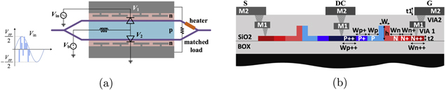
Figure 7. (a) Schematic of a TW-MZM in the series push-pull driving configuration with a PAM-4 driving signal; T-shaped extensions are used in the CPS TW electrode to slow-down the RF signal and improve the velocity matching between RF and optical signals. A common reverse bias is applied on the two back-to-back waveguide diodes through a bias tee. (b) Cross-sectional schematic of a lateral pn-junction waveguide in (a) using a generic SiP process (CMC-IME MPW): Wp++ = 5.2, Wp+ = 0.83, Wp = 0.37, Wn++ = 5.2, Wn+ = 0.81, Wn = 0.39, W = 0.5, h = 0.22, t1 = 2, t2 = 0.9 (all the dimensions are in μm). © 2017 IEEE. Reprinted, with permission, from [14].
Download figure:
Standard image High-resolution image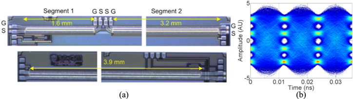
Figure 8. (a) Micrograph of a dual-segment (BWS) MZM (top) and a TW-MZM (bottom); (b) 84 Gbaud PAM- 4 eye diagram of the dual-segment MZM. Reproduced with permission from [50] (Optical Society of America).
Download figure:
Standard image High-resolution imageTable 1. Performance of state-of-the-art SiP MZMs and EAMs for PAM.
| References | Type/Process | Format | Raw Gb s−1 (FEC overhead) | Link | DSP | Vpp | EC (pJ/bit)a |
|---|---|---|---|---|---|---|---|
| [50] | BWS TW-MZM/Lateral-pn | PAM-4 | 168 (KP4) | B2B | TX and RX | 3 (LSB)/4 (MSB) | N.A. |
| 128 (KP4) | 1 km | TX and RX | 0.41 | ||||
| 100 (KP4) | 1 km | No | 0.46 | ||||
| [68] | BWS TW-MZM/Lateral-pn | PAM-8 | 114 (7%) | B2B | RX | 3.5/3.5/4 | N.A. |
| [15] | TW-MZM/Lateral-pn | PAM-4 | 112 (7%) | 2 km | TX and RX | 5.21 | 0.18 |
| PAM-8 | 5 km | 0.35 | |||||
| [32] | TW-MZM (O-band)/Lateral-pn | PAM-4 | 112 (7%) | 20 km | TX and RX | 2.85 | N.A. |
| PAM-8 | 3.2 | ||||||
| [69] | Dual-Parallel TW-MZM/Lateral-pn | PAM-4 | 100 (7%) | 2 km | No | 2 (LSB)/4 (MSB) | N.A. |
| [35] | GeSi EAM/Lateral-pin (FKE) | PAM-4 | 112 (7%) | 2 km | TX and RX | 1.15 | N.A. |
| [67] | GeSi EAMs in parallel/Lateral-pin (FKE) | PAM-4 | 112 (7%) | 2 km | No | 1.1 (LSB)/2.2 (MSB) | N.A. |
aOnly the energy consumed on optical modulation is considered. Other power-consumption contributions such as DAC, DSP, and static power on modulator biasing are not included.
Using a TW-MZM and a high-resolution DAC allows for flexible generation of various modulation formats. In this case, the optical modulation bandwidth is limited by RF losses due to the large junction capacitance [70]. The series single-drive push-pull configuration (figure 7(a)) is widely used to reduce the capacitance for a higher bandwidth and to reduce the number of RF connections at the expense of a higher driving voltage compared to the dual-drive push-pull configuration [42, 70, 71]. Many SiP PAM MZMs have adopted this configuration. Optical PAM-4 generation using a carrier depletion TW-MZM was first reported in [72], where an electrical DAC provided a 4-level signal to feed the optical modulator for up to 20 Gbaud. The speed was pushed to 112 Gb s−1 (56 Gbaud PAM-4) by optimizing the electrode design and the bias of the junction [15, 73]. PAM-8 was also examined [15, 73]. While PAM-4 can effectively increase the bit rate compared to OOK, PAM-8 usually does not lead faster transmission due to requirement for significantly higher SNR. In currently available technologies, PAM-4 seems to provide the best trade-off between spectral efficiency and SNR. To further increase the bandwidth, Li et al showed that removing the silicon substrate could effectively reduce the RF loss [74]; 64 Gbaud PAM-4 (128 Gb s−1) was achieved. An O-band SiP TW-MZM showed the capacity of 112 Gb s−1 PAM-4 and PAM-8 transmissions over 10 km when applying digital pre- and post-compensation [32]; dual-polarization of 224 Gb s−1 over 10 km was also demonstrated using MIMO DSP [75].
To overcome the compromise between bandwidth and Vπ of TW-MZM, the binary weighted coded segmentation (figure 5(c)) has been intensively examined [50, 51, 76]. The DAC-less operation also eliminates the noise and bandwidth limitation of an electrical DAC. Capable of generating multi-level signal in the optical domain using binary electrical inputs, this type of optical modulator is sometimes referred as an optical or electro-optical DAC, although not everyone agrees on this terminology. In this scenario, the single-drive series push-pull configuration is also popular to minimize the required RF driving signals. The bandwidth is typically limited by the longest segment (for the MSB). Delay between the driving signals needs to be carefully tuned to match the optical delay. For PAM-4, up to 168 Gb s−1 generation and 128 Gb s−1 transmission over 1 km have been demonstrated [50] (shown in figure 8). In [76], the authors compared three structures in the same fabrication process for PAM-4 generation and transmission: single MZM, dual-parallel MZM and dual-segment (BWS) MZM, all using the similar TW electrode design. The dual-parallel structure is a special case of the parallel AM architecture (figure 6(b)) where the optical input is equally split (α = 0.5). Their results showed that the BWS structure had superior performance over the other two. However, it should be noted that the dual-parallel structure may be further improved, e.g. by optimizing the input splitting ratio. Towards an even higher spectral efficiency, a three-segment MZM for PAM-8 was demonstrated (figure 9) [51], by which 114 Gbps (38 Gbaud PAM-8) has been achieved.
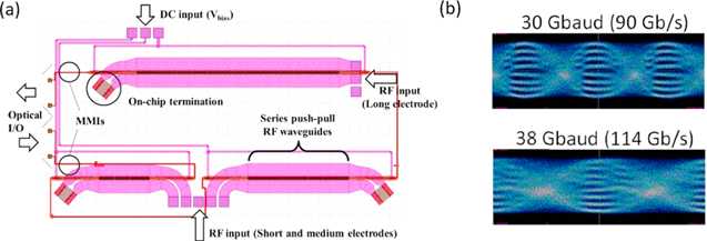
Figure 9. (a) Layout schematic of the PAM-8 MZM with three segments (0.5, 1, and 2 mm in length, respectively) each applying a TW electrode; (b) 30 Gbaud and 38 Gbaud PAM-8 eye diagrams with 5 dBm received power. The device was reported in [51].
Download figure:
Standard image High-resolution image4.2. Resonator-based modulators for PAM
Resonator-based modulators are appealing for optical interconnects due to their low energy consumption and high bandwidth-density. Several groups have studied PAM-4 transmission using single MRMs with an electric DAC or AWG [17, 77–79]. With an ultra-compact footprint (on the order of 10 μm in radius), they have shown good performance, comparable to MZMs. Net data rates up to 120 Gb s−1 for PAM-4 [80] and 42 Gb s−1 for PAM-8 [17] have been achieved, indicating two to three orders of bandwidth-density enhancement. Transmissions over single-mode fibers ranging from a few hundred meters up to 150 km have been demonstrated [77]. Their dynamic energy consumptions are also orders of magnitude smaller than MZMs (down to 1 fJ/bit [17]). However, the need for thermal tuning and stabilization raises the total power consumption to the level of 100 fJ/bit [17]. Some recent PAM results achieved using resonator-based SiP modulators are listed in table 2.
Table 2. Performance of state-of-the-art SiP MRMs for PAM.
| References | Type/Process | Format | Raw Gb s−1(FEC overhead) | Link | DSP | Vpp (V) | EC (fJ/bit)a |
|---|---|---|---|---|---|---|---|
| [17] | MRM/Lateral-pn | PAM-4 | 80 (7%) | B2B | Rx | 3.5 | 7 |
| PAM-4 | 64 (7%) | 5 km | Rx | 3.5 | 7 | ||
| PAM-8 | 45 (7%) | B2B | No | 2.2 | 1 | ||
| [80] | MRM/Lateral-vertical-pn | PAM-4 | 128 (N.A.) | B2B | No | 2.4 | N.A. |
| [37] | Dual-MRM in serial/Lateral-pn | PAM-4 | 60 (7%) | B2B | Rx | 2 (LSB)/5 (MSB) | 45 |
| [81] | Dual-MRM in parallel/Lateral-pn | PAM-4 | 50 (7%) | 2 km | No | 3.19 (LSB)/4.26 (MSB) | N.A. |
| [68] | Dual-phase-shift IBG /Lateral-pn | PAM-4 | 60 (7%)) | B2B | Rx | 3.19 (LSB)/4.26 (MSB) | N.A. |
aOnly the energy consumed on optical modulation is considered. Other power-consumption contributions such as DAC, DSP, and static power on wavelength tuning and stabilization are not included.
Figure 10(a) shows a compact MRM design in an all-pass configuration consisting of a bus waveguide coupled to a single microring resonator that is partially doped for intra-cavity modulation. The device was demonstrated by Dubé-Demers et al in 2016, having achieved up to 80 Gb s−1 PAM-4 transmission with an ultra-low-power consumption below 7 fJ/bit [17]. The MRM showed a very high ER of 35 dB (figure 10(b)), which was important for achieving high-order PAM modulation. The choice of the optimal operating point was a result of the trade-off between modulation efficiency and bandwidth. The output of the DAC was pre-distorted to linearize the optical output of the PAM signals. Figures 10(c) and (d) show the measured eye diagrams for PAM-4 up to 40 Gbaud (80 Gb s−1) and PAM-8 up to 15 Gbaud (45 Gb s−1) with a 7% FEC overhead. The power consumed by optical modulation was estimated to be as low as 1 fJ/bit and 6.5 fJ/bit for PAM-8 and PAM-4, respectively. A detailed methodology of characterizing the performance and energy consumption (RF and thermal tuning) of an MRM for PAM is also provided in [17].

Figure 10. (a) Partial layout of the mask used for the fabrication of the device; (b) measured power transmission spectra in the vicinity of a resonance; (c) eye diagrams of the equalized PAM-4 at 80 Gb s−1; (d) eye diagrams of the equalized PAM-8 at 45 Gb s−1. The received power is 7 dBm. Reproduced with permission from [17] (Optical Society of America).
Download figure:
Standard image High-resolution imageBy optimizing MRM design and increasing the EO bandwidth, data rates above 100 Gb s−1 per wavelength are possible. Most recently, Sun et al [80] demonstrated an MRM with pn junction in both vertical and horizontal directions for a very high modulation efficiency (0.52 V cm). The device showed a high EO bandwidth of 50 GHz and enabled 128 Gb s−1 PAM-4 modulation in the O-band with a 7% FEC overhead, as shown in figure 11. This result is impressive considering that no electrical equalization was used. Wavelength tuning with an efficiency of <20 mW/π over a full free-spectral range was also demonstrated.
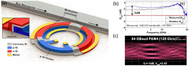
Figure 11. (a) A schematic of an MRM with a close-up view of the pn junction; (b) measured EO response (S21) of the MRM, showing an EO bandwidth of 50 GHz, (c) 128 Gb s−1 PAM-4 (64 Gbaud). No electrical equalization was applied to MRM. Reproduced with permission from [80] © 2018 The Author(s).
Download figure:
Standard image High-resolution imageSimilar to the segmentation of the electrodes in an MZM to realize an optical DAC, several groups [82–84] have investigated segmentation of phase shifters in a MRM. To implement PAM-4 modulation with a single MRM driven by two simple NRZ drivers, the MRM is modified by utilizing two phase shifters with a longer MSB segment and a shorter LSB segment as shown in figure 12(a). Two-level control of the two phase shifters allows the device to operate as a 4-level optical DAC The MSB:LSB length ratio is optimized for PAM-4 modulation considering the same nominal 2-level 4.4 Vp−p drive voltage. As shown in the measured linear scale transmission curves of figure 12(b), a 1.9:1 ratio allows for uniform level spacing with the laser wavelength slightly offset from the resonant frequency. Measured 40 Gb s−1 PAM-4 optical eye diagrams at the output of the segmented microring device are shown in figure 12(c) for the optical DAC transmitters.
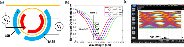
Figure 12. (a) Top view of the segmented MRM; (b) measured normalized transmission curves of the segmented MRM with different reverse bias voltages applied to the MSB and LSB segments; (c) measured 40 Gb s−1 PAM-4 optical eye diagrams from the optical DAC transmitters. © 2017 IEEE. Reprinted, with permission, from [83].
Download figure:
Standard image High-resolution imageConsidering an MRM as a binary AM, as discussed in section 3, there are two methods to achieve PAM-4 modulation by independently modulating two MRMs with uncorrelated PRBS: MRMs in series [37, 85–87] and MRMs in parallel [81]. In 2016, Dubé-Demers et al, demonstrated a low-power DAC-less 60 Gb s−1 PAM-4 transmitter in cascaded dual MRMs [37]. The two MRMs are coupled in series to the same bus waveguide in an all-pass configuration, as shown in figure 13(a). The four states needed to produce the PAM-4 signal are clearly visible in the measured spectra of the modulator when the resonances were aligned, figure 13(b). Measured eye diagrams of the optical DAC based on MRMs at 60 Gb s−1 are shown in figure 13(c). In 2017, Li et al [81] demonstrated DAC-less and DSP-free PAM-4 transmission at 50 Gb s−1 in two MRMs in parallel, figure 14(a). PAM-4 is generated by modulating the two MRMs at different voltages. The power transmission of the modulator under the four combinations of the applied voltages is shown in figure 14(b) where the four power transmission levels have even spacing at the reference wavelength. The measured PAM-4 eye diagrams at 25 Gbaud after 2 km of SSMF transmission is shown in figure 14(c).

Figure 13. (a) Schematic of the cascaded dual MRMs; (b) measured transmission spectra illustrating the four different states used in the PAM-4 demonstration. The vertical line shows the position of the laser used; (c) eye diagrams of the equalized PAM-4 signals at 60 Gb s−1. The eye samples are taken at 5 dBm of received power. Reproduced with permission from [37] (Optical Society of America).
Download figure:
Standard image High-resolution image
Figure 14. (a) Structure of the RAMZI, schematic of the PN junction; (b) power transmission of the silicon RAMZI at the four combinations of the applied voltages; (c) 25 Gbaud PAM-4 after 2 km of SSMF. © 2017 IEEE. Reprinted, with permission, from [81].
Download figure:
Standard image High-resolution imageBesides MRMs, other resonant structure such as integrated Bragg gratings (IBG) can also be advantageously used to make SiP modulator more compact and to lower power consumption. Single or coupled resonators can be used as stand-alone modulators, or they can be combined in MZI structures to shorten the length and improve the efficiency of MZ-based modulators. Resonance phenomena typically have a narrow bandwidth and their amplitude response is accompanied by phase change that results in modulation chirp. In [68], Bedard et al studied a push-pull IBG modulator with dual-phase-shifts that can overcome this effect. Cascaded resonator structures can also provide a wider bandwidth, which decreases the temperature sensitivity of the modulator. Two phase-shifts were positioned to produce a transmission peak with a 3 dB bandwidth of ∼0.2 nm. The optical carrier is positioned at the central wavelength of the transmission peak and amplitude modulation is obtained by tuning the grating regions with the two phase shifts in opposite direction (push-pull operation). Figure 15 shows a schematic of the structure and the test setup. PAM-4 transmission results up to 30 Gbaud (60 Gbit s−1) were achieved.
Figure 15. (a) Schematic of the IBG modulator; (b) typical spectra with/without bias voltages applied to the PN junctions and a typical spectrum for a Bragg grating with a single p phase-shift; (c) back-to-back BER measurement results of PAM-4 up to 30 Gbaud with (lower curves) and without (upper curve) equalization. Reproduced with permission from [68] (Optical Society of America).
Download figure:
Standard image High-resolution image4.3. EAM for PAM transmission
As a CMOS-compatible material system, GeSi has a strong electro-absorption (EA) effect which is intrinsically an ultrafast process, enabling high-speed modulation. The EA effect is known as the FranzKeldysh effect (FKE) in bulk semiconductors and the quantum-confined Stark effect in quantum-well structures. The FKE enables the modulation of the absorption coefficient of bulk Ge by an applied electric field near the direct band gap of Liu et al [88] first demonstrated a GeSi FK modulator integrated on a submicron silicon waveguide using a pin junction operated in reverse bias. GeSi based EAMs have smaller footprint and lower power consumption than MZMs, and higher optical bandwidth than MRMs. Typically, Ge EAMs work in L-band (around 1600 nm) and could be shifted to C-band (1550 nm) with the incorporation of Si during Ge epitaxial growth. However, at these wavelengths, the relatively large chromatic dispersion coefficient may induce notches in the frequency response of optical link which limits the maximal fiber span without chromatic distortion compensation techniques.
Recently, El-Fiky et al [35] demonstrated 112 Gb s−1 (56 Gaud) PAM-4 modulation in a C-band GeSi EAM with a DAC The EAM was fabricated on the IMEC SiP platform on a 200 mm silicon-on-insulator wafer with 220 nm top Si thickness and it consists of a 600 nm wide and 40 μm long germanium waveguide with an embedded pin junction, the cross-section and layout is shown in figure 16(a)). To obviate the electrical DAC and power-hungry DSP, Verbist et al [67] generated 112 Gb s−1 PAM-4 by the vector addition of two binary driven EAMs in parallel. The transmitter based on this topology was fabricated using two identical 40 μm long GeSi EAMs, driven with two NRZ streams at 1.1 Vp−p and 2.2 Vp−p for the LSB and MSB, respectively. Clear, open eyes were obtained with the LSB or the MSB EAM driven singly, as well as when driving both EAMs simultaneously at 56 Gbaud. The cross-section of the GeSi EAM and the eye diagrams are shown in figure 16(b).

Figure 16. (a) Cross-section and layout of the waveguide-integrated GeSi EAM; (b) received optical eye diagrams from EAMs in parallel with only the LSB or the MSB EAM driven, and with both EAMs driven at 56 Gbaud (112 Gb s−1). (a) Reproduced with permission from [89] (Optical Society of America). (b) © 2018 IEEE. Reprinted, with permission, from [67].
Download figure:
Standard image High-resolution image
Figure 17. Demonstrations of electronic-photonic integrated PAM-4 transmitters: (a) monolithic integration of a 2-segment MZM and a CMOS driver using a 90 nm CMOS process [90]; (b) a segmented MRM and a hybrid integrated driver in 65 nm CMOS [83]. (a) Reproduced with permission from [90] (Optical Society of America). (b) © 2017 IEEE. Reprinted, with permission, from [83].
Download figure:
Standard image High-resolution image
4.4. Electronic-photonic integrated transmitters
Co-design and integration of optical modulators and CMOS or BiCMOS drivers for high-speed silicon photonic transmitters may reach their full potential for low-cost, low-power electronic-photonic integrated systems. Advanced submicron CMOS processes have voltage outputs less than 2 V, which is low compared to the Vπ of optical modulators in a generic silicon photonic process. Innovative designs (e.g. [91]) in both electronic circuitry and SiP have been employed to address this challenge. Some recently demonstrated integrated SiP PAM transmitters are listed in table 3.
Table 3. Performance of state-of-the-art SiP PAM-4 transmitters.
| References | Modulator type—process/CMOS process | Raw Gb s−1 (FEC overhead or BER) | Link | DSP | EC (pJ/bit)a |
|---|---|---|---|---|---|
| [83] | Segmented MRM—Lateral-pn/65 nm CMOS | 40 (BER < 10−12) | B2B | No | N.A. |
| [90] | BWS TW-MZM—Lateral-pn/Monolithic CMOS9WG | 56 (7%) | 500 m | No | 4.8 |
| [92] | UWS MZM—Lateral-pn/ Monolithic 250 nm BiCMOS | 50 (7%) | B2B | No | 30 |
| [93] | BWS MZM—SISCAP/ N.A. | 45 (BER < 10−10) | 10 km | No | N.A. |
| 51.2 (BER < 10−9) | B2B | N.A. | |||
| [36] | UWS MZM—Lateral-pn/ Hybrid 130 nm CMOS | 38 (7%) | B2B | Rx | 9.8 |
| 28 (7%) | No | 9.8 |
There are several demonstrations of CMOS-SiP co-design and integration for low-power SiP transmitters [94–96]. In [36], the authors presented a DAC-less SiP PAM-4 transmitter (using lateral pn-junction) and its co-designed CMOS driver and delay controller in 130 nm CMOS, achieving 38 Gb s−1. The performance of the transmitter was limited by the low analog bandwidth of the CMOS driver. It showed that delay management between the segments in the transmitter is a critical concern that should be addressed properly to benefit from the wide EO bandwidth of the segmented MZMs. Moving to deep submicron CMOS processes, more flexible and power efficient transmitters were presented. In [97], a flexible transmitter employing segmented MZM and its distributed CMOS driver in 32 nm CMOS is reported, where on-chip optical equalization was performed to improve transmitter performance. In [93], 25.6 Gbaud DAC-less PAM-4 error-free transmissions over 10 km SMF and 100 m MMF at 1310 nm were achieved using a segmented MZM and its co-designed CMOS driver packaged in a QSFP module. It applied the SISCAP phase shifter that enables a better overlap between the optical mode and the electric field, which can effectively reduce the driving voltage for integration with low-power CMOS drivers [98] and can shorten the length of phase shifter, eliminating the need for a TW electrode [10].
Beside the hybrid integration of CMOS and SiP chips, several studies achieved monolithic integration of electronic and photonic integrated circuits [90, 92, 95, 99]. In [90], a monolithic 56 Gb s−1 PAM-4 transmitter is presented where the CMOS driver circuitry and segmented TW-MZM were fabricated on the same wafer. Higher voltage-swing and faster transistors available in BiCMOS pave the way for demonstration of BiCMOS driver and SiP modulator co-design for PAM-M modulation format [92, 99]. In [92], a monolithic integration of the driver and optical PAM-4 modulator in BiCMOS process was presented running at 50 Gb s−1. While its power consumption (30 fJ/bit) is higher than the CMOS solutions [90, 94–96], a very large ER (up to 13 dB) was achieved with a long MZM concept.
5. Outlook and conclusion
Through years of intensive research and development, researchers and engineers have developed in-depth understating of the capacity, design and performance trade-offs of SiP modulators on generic integration platforms for high-speed PAM transmissions. The state-of-the art lab experiments have achieved net rates well beyond 100 Gb s−1 with dynamic energy consumed on the photonic chip at the level of 100 fJ/bit (including high-frequency modulation and low-frequency tuning). Although challenging, further optimization (e.g. improving the tuning efficiency of MRMs) may push the modulator energy efficiency to the level of 10 fJ/bit. With an energy consumption below 1 pJ/bit, integrated CMOS-SiP PAM transmitters have achieved 56 Gb s−1 and should soon go beyond 100 Gb s−1. SiP PAM-4 WDM transceivers beyond 400 Gb s−1 (4λ × 56 Gbaud or 8λ × 28 Gbaud) are promising.
For next generations of optical links, targeting terabits or even petabits, putting aside wavelength and spatial multiplexing, optical modulators should run at much higher baud rates with higher modulator formats. The quality of higher-order PAM signals (such as PAM-8 and PAM-16) can be further enhanced depending on the improvement of insertion loss and ER. Future optical interconnects may eventually adopt coherent detection, or direct detection with either intensity modulation or complex modulation (e.g. Kramers–Kronig detection [100]). In any case, the main limiting factor of SiP modulators remains the weak modulation efficiency that hinders further reduction of energy consumption. Various pn-junction structures [16, 101] and waveguide designs (e.g. slow light [102]) have been examined for improved efficiency. Recent breakthroughs in hybrid integration of heterogeneous materials [103], such as III–V compound semiconductors [104, 105], plasmonic materials [106], polymers [107], and graphene [108] have shown great potential for orders-of-magnitude efficiency enhancement. The driving topologies already developed can naturally be adopted by new modulators for PAM transmissions. Higher efficiency can certainly help simplify the design of driving circuits and reduce the form factor of integrated transceivers. Nevertheless, incorporating new materials into the large-wafer SiP manufacturing processes is challenging. III–V compound materials are likely to be first adopted in a generic SiP process due to the urgent need for on-chip amplifiers and lasers. In addition, more thorough investigation is needed, e.g. using the bandwidth-aware FOM [14], to verify if and how much these new structures and hybrid processes can improve the link power budget.
As a young technology, SiP is still evolving quickly [109]. SiP modulators will continue advancing along with the process and platform, as well as further advances in low-power CMOS and packaging technologies. Note that the current data center and HPC markets are still dominated by multi-mode VCSELs due to their cost advantage for single-channel transceivers [110]. Beyond 50 Gb s−1 PAM in VCSESLs has been demonstrated [111]. SiP will be more competitive as the channel rate and the average link length continue to increase, especially in mega data centers where single-mode fibers are used in structured cabling. As the technology becomes mature and more adaptive, new optical modulation techniques and algorithms will be examined on the silicon platform. Looking to the next decade, we are optimistic that SiP-based optical links will quickly expand in data centers and HPC systems. Recent breakthrough in monolithic electronic-photonic integrated systems [112] reveals promise to adopt the high-speed SiP PAM links for even shorter-reach communications inter- and intra-microchips.