
Abstract
The ability to process optical signals without passing into the electrical domain has always attracted the attention of the research community. Processing photons by photons unfolds new scenarios, in principle allowing for unseen signal processing and computing capabilities. Optical computation can be seen as a large scientific field in which researchers operate, trying to find solutions to their specific needs by different approaches; although the challenges can be substantially different, they are typically addressed using knowledge and technological platforms that are shared across the whole field. This significant know-how can also benefit other scientific communities, providing lateral solutions to their problems, as well as leading to novel applications. The aim of this Roadmap is to provide a broad view of the state-of-the-art in this lively scientific research field and to discuss the advances required to tackle emerging challenges, thanks to contributions authored by experts affiliated to both academic institutions and high-tech industries. The Roadmap is organized so as to put side by side contributions on different aspects of optical processing, aiming to enhance the cross-contamination of ideas between scientists working in three different fields of photonics: optical gates and logical units, high bit-rate signal processing and optical quantum computing. The ultimate intent of this paper is to provide guidance for young scientists as well as providing research-funding institutions and stake holders with a comprehensive overview of perspectives and opportunities offered by this research field.
Export citation and abstract BibTeX RIS

Original content from this work may be used under the terms of the Creative Commons Attribution 3.0 licence. Any further distribution of this work must maintain attribution to the author(s) and the title of the work, journal citation and DOI.
List of Acronyms
| 3PA | Three photon absorption |
| ADC | Analogue-to-digital converter |
| AlGaAs | Aluminum gallium arsenide |
| AO-OFDM | All-optical orthogonal frequency division multiplexing |
| ASE | Amplified spontaneous emission |
| a-Si:H | Hydrogenated amorphous silicon |
| CD | Chromatic dispersion |
| CDR | Clock and data recovery |
| CMOS | Complementary metal-oxide semiconductor |
| CNOT | Controlled NOT |
| CVD | Chemical vapor deposition |
| CW | Continuous wave |
| DAC | Digital-to-analog converter |
| DC | Data centre |
| DCN | Data centre network |
| DPSK | Differential phase-shift keying |
| DSP | Digital signal processing |
| EDFA | Erbium-doped fiber amplifier |
| EVM | Error vector magnitude |
| FEC | Forward error code |
| FFT | Fast Fourier transform |
| FWM | Four-wave mixing |
| GaAs | Gallium arsenide |
| HOMs | Higher order modes |
| I/O | Input/output |
| ICT | Information and communications technology |
| InGaAs | Indium gallium arsenide |
| InP | Indium phosphide |
| KLM | Knill Laflamme and Milburn |
| MMFs | Multi-mode fibres |
| MWP | Microwave photonics |
| MZ | Mach-Zehnder |
| MZI | Mach-Zehnder interferometer |
| NF | Noise figure |
| NRZ | Non return to zero |
| OEO | Optical/electrical/optical |
| OFDM | Orthogonal frequency division multiplexing |
| OOK | On-Off keying |
| OSNR | Optical signal-to-noise ratio |
| OTDM | Orthogonal time division multiplexing |
| PAM | Pulse amplitude modulation |
| PDL | Polarization dependent loss |
| PIC | Photonic integrated circuit |
| PLA | Programmable logic array |
| PMD | Polarization mode dispersion |
| PSA | Phase-sensitive amplifier |
| PSK | Phase-shift keying |
| QAM | Quadrature amplitude modulation |
| QD | Quantum dot |
| QIP | Quantum information processing |
| QND | Quantum non-demolition |
| QPSK | Quadrature phase-shift keying |
| RF | Radio frequency |
| ROADM | Reconfigurable optical add/drop multiplexer |
| RZ | Return to zero |
| SDM | Space-division multiplexing |
| SFDR | Spurious-free dynamic range |
| SNR | Signal-to-noise ratio |
| SOA | Semiconductor optical amplifier |
| SOI | Silicon-on-insulator |
| SoP | State of polarization |
| SPM | Self-phase modulation |
| SPP | Surface plasmon polariton |
| TE | Transverse electric |
| TIDE | Terabit interferometric add, drop, and extract |
| TM | Transverse magnetic |
| TPA | Two-photon absorption |
| WDM | Wavelength division multiplexing |
| WGM | Whispering gallery mode |
| WSS | Wavelength selective switch |
| XAM | Cross-absorption modulation |
| XGM | Cross-gain modulation |
| XPM | Cross-phase modulation |
| XPolM | Cross-polarization modulation |
1. Introduction
Paolo Minzioni1and Cosimo Lacava2
1University of Pavia, Pavia, Italy
2Optoelectronics Research Centre, Zepler Insitute, University of Southampton, Southampton, United Kingdom
The importance of all-optical processing
The advent of the current era (often regarded as the 'information age') has been enabled by the capability of transferring and processing large quantity of information in a relatively small amount of time. Specifically, while data are generally encoded on photons for transmission, the information is then converted to the electronic domain for the processing phase. This is related to a fundamental difference between electrons and photons: electrons can strongly interact with each other even in vacuum, while photon–photon interactions require the presence of a suitable medium to enable such an interaction. For this reason, electronic systems are generally used to perform signal processing and nonlinear operations facilitating the implementation of Boolean logic ports. On the other side, optical carriers (with a frequency generally between 150 and 3000 THz) are used to transmit data over hundreds of km, at a very high bit rate, and without the need of any regeneration stage.
The bandwidth and the noise performance of photon-based systems have rapidly fueled the research on optically-operated computing systems, and considerable research efforts have been devoted to it in the past [1, 2]. However, the lack of efficient measures to achieve photon-to-photon interactions has restricted the ambition of this research field, and computers have evolved using CMOS electronic technologies, reaching the technology level we all know.
Although the idea of fully-optical processors and computers seems to be abandoned, optical processing has been identified as a possible answer to many problems modern society is currently facing. Indeed, the increasing complexity of scientific and mathematical problems, as well as the need for novel superfast and mass-producible components for telecommunication and sensing applications, justify the necessity of all-optical components able to manipulate signals at ultra-fast speed levels (>500 Gb s−1). Intensive research in optical quantum computing and deep-learning applications are only two examples of this new research trend [3, 4].
In telecommunication, fully-optical devices with few-fs response times are crucially needed to enable the realization of optical networks with transmission capacity exceeding the Tb/s. In contrast to the past, thanks to the significant technological developments that have occurred during the last few decades, efficient all-optical signal processing devices can nowadays be realized and their reliability level is now sufficient to allow possible integration with the existing fiber optic infrastructure.
Integrated platforms, such as those based on lithium-niobate, indium phosphate, silicon, silicon oxide and silicon nitride, have rapidly developed in the last 10 years, allowing scientists to demonstrate the basic set of functionalities needed in a standard optical network, namely signal switching, routing, wavelength and format conversion, phase conjugation, phase sensitive amplification, time-lens based optical Fourier transformation and signal regeneration (amplitude and phase) [5–21]. The significant development of integrated platforms also allowed the realization of devices composed by many single, interconnected components, reaching unprecedented levels of complexity.
This is particularly true for semiconductor-based platforms where a high-index contrast between waveguides' core and cladding is realized, as it happens in silicon on insulators and silicon nitride, as well as indium phosphide. Recently, a lot attention has also been paid to materials not commonly used in the fiber communication field, e.g. diamonds [24], which could find a specific usage in quantum processing devices and systems. Even if the advancements in the semiconductor-photonics area play a fundamental role in this field, it is important to recall that the performance of fiber-based devices still remain unsurpassed in some cases [22–24]. This unveils alternative scenarios, in which fiber- and semiconductor-based devices coexist. Indeed, significant research efforts are currently devoted to the development of novel fiber structures (e.g. silicon-core fiber) with tailored-nonlinearities, so as to reduce the fiber length and optical power required to obtain efficient signal processing.
Although significant advances were recently demonstrated, further developments are still needed to bring these devices into real settings, but a new-era of all-optical signal processing now seems possible, opening up exciting perspectives for the future of global communications and for computing systems.
Roadmap organization and aim
In order to give the readers a comprehensive overview of the field and to encourage cross-contaminations between different research directions while maintaining high readability, we decided to divide the Roadmap in three different sections, devoted to optical logic units and gates, signal processing for telecom applications and quantum processing, respectively.
The primary purpose of this document is to reflect the current state of the art of the field, eventually identifying the main challenges that have to be overcome by the research community, in order to bring all-optical signal processing devices into real optical networks and computing settings. It is worth noting that the authors of the Roadmap were well aware of the impossibility to produce a fully exhaustive document in such a wide and rapidly evolving field. Nevertheless, we believe that the included contributions represent a relevant picture of the current state of the art and of recent trends, thus proving itself as a useful read for many scientists. The intended audience of this document includes students and young researchers that are approaching the topic, as well as experienced professionals looking for a reference on the current state of the art in this field.
Open challenges
In such a varied field, each research line has a specific set of challenges to be faced in the near future, allowing for the development of functional optical processing solutions. Nevertheless, it is interesting to note that there are a few recurring topics cited and analyzed in the following Roadmap contributions.
Here, we briefly list and describe the main common-challenges, so as to stress their importance, and we invite the reader to pay attention to two aspects while reading the different contributions: (i) the impact of similar problems to the different research lines and (ii) the different approaches used by scientists to decipher similar scientific questions.
1. Platforms
Traditionally, the development of all-optical-processing functions was focused on the development of discrete blocks, with limited or no integration among them. Nowadays, the ability to combine diverse functions in a single device is considered to be fundamental. As a result, researchers have been focusing their attention on the development of suitable platforms (i.e. material, technology and operating conditions) for the integration of optical and electro-optical components, enabling the realization of integrated solutions [25].
2. Power consumption
The exploitation of optical nonlinear effects for signal processing purposes naturally implies the need for high-intensity beams and thus the use of a relatively high-power optical source. Although different solutions have been proposed, and others are being investigated, the limitation on power consumption could drastically affect the performance of signal processing systems [26].
3. Killer applications
Some of the currently ongoing research activities in the field of optical processing are vaguely reminiscent of the research activities which were being developed in the late 50s about the development of laser sources. Although there is an almost unanimous consent about their relevance, the specific applications which could be developed in the future and the specific fields where optical computing could become the reference standard are somewhat undefined [27].
4. Losses
As has often occurred in the development of optical applications, since the first study on optical fibers, the reduction of optical losses (both those connected to absorption and scattering) is a fundamental issue [28]. This aspect is even more relevant in two extreme regimes: high optical beam power (as it significantly impacts the device power budget) and single-photon applications (where low losses are required for proper signal collection). Both of these two regimes are of extreme interest for optical processing, as will be evident by reading the Roadmap contributions.
5. Tuning
With the development of large bandwidth communication systems, it is becoming more and more important to realize signal processing systems able to fully exploit the fiber communication spectrum [29–31]. Additionally, the ongoing development of highly efficient sources (and other components) working at different wavelengths implies the necessity of suitable wavelength-conversion systems, so as to guarantee the compatibility of the newly developed components with the existing and standardized fiber infrastructure for optical communications [32].
6. Coupling
Another challenge commonly encountered in the development of integrated all-optical processing systems is represented by the development of efficient interface systems, between the realized component and the external components (i.e. fiber optic network). This issue, covering both the ability to inject the optical radiation in the integrated components and the ability to efficiently collect the photons emitted by the optical sources, is also currently receiving a lot of attention, even for integrated optical components not devoted to signal processing [33, 34].
Current general trends
The solutions given, or envisaged, for the above reported issues are, as can be expected, strongly dependent on the considered applications, approaches and targets. Quite surprisingly, there are a few common solution-trends which often emerge as promising research directions in many fields. We thus want to conclude this introduction by highlighting the relevance of three aspects.
1. Integration
The integration trend includes two largely different directions: monolithic integration and heterogeneous integration. In the first case, the target is to realize as many functions as possible within the same substrate material. In the second case, the approach is to define suitable strategies and designs that allow the possibility of integrating a different material within the main substrate. This solution makes it possible to take advantage of materials with different properties to implement specific optical functions, thus offering an additional degree of freedom for the device design.
2. Materials modification
In order to optimize the materials' optical properties, a commonly envisaged strategy is to modify the material properties, by realizing metamaterials, multilayers or stressed structures. These solutions, acting both on the physical material structure and on the control of the light–matter interaction, allow the tuning of the materials' linear and nonlinear properties, thus enabling the possibility to fine tune the material response. As an example of the large changes which can be introduced by proper material modification, it is worth mentioning the creation of a non-negligible χ(2) coefficient in Si-waveguides by different techniques, such as E-field [31] or surface straining [35, 36], and the enhancement of χ(2) nonlinearities in Si3N4 waveguides by optically-written photogalvanic gratings [37].
3. Fabrication technologies
One of the most promising trends for the development of innovative devices relies on the development of new fabrication technologies, either enabling the realization of structures not currently achievable (both as structure definitions and optical performance), or allowing us to exploit the optical properties of different materials [38–40].
LOGIC UNITS AND GATES
2. Cavity-based all optical flip-flops and logic gates
Takasumi Tanabe
Keio University, Japan
Status
All optical flip-flops and logic gate devices have been studied for decades with the expectation of realizing faster speed and lower energy consumption by replacing electrical circuits with photonic circuits. Particularly, they could be used in optical routers where signals are transmitted with light.
The key feature, first observed in 1974, is optical bistability, where a cavity and a nonlinear medium are usually employed [41]. Subsequently, the phenomenon has been used to achieve various optical logic gate operations in photonic devices.
In the late 1980s, all-optical flip-flop operation was demonstrated using nonlinear Fabry-Pérot etalons (see, for example, [42]). These studies realized all-optical logic operation, and it was expected that all-optical computing would soon become a reality. However, it was soon realized that there were still many obstacles preventing the development of a practical system. The device is large and bulky, which makes integration impossible. In addition, the device operates at a high input power because of the high intensity electrical field needed to achieve optical nonlinearity. These problems make the device difficult to employ practically, and new technologies must be developed if we are to obtain integrated photonic systems.
The circumstances changed rapidly when nano-fabrication technologies made significant progress in the 1990s. The key device needed to achieve low-power all-optical logic gate operation is a high Q/V cavity, where Q is the quality factor and V is the mode volume. The field intensity inside a cavity at a given input power scales with Q/V, so it is now possible to obtain a strong field intensity and utilize optical nonlinearities at a low input power. The development of the III-V and silicon high-Q microcavities on a chip made it possible to demonstrate low-power cavity-based all-optical logic gates.
In early 2000, a number of experimental demonstrations of bistable switching were reported using active [43] and passive [44, 45] microcavity based devices. By utilizing active microring lasers, bistable switches such as those capable of clockwise-anticlockwise switching [43] were demonstrated, where triggering was achieved with an energy of only a few fJ (10−15 J). Optical flip-flops are demonstrated with passive microcavities that are even more suitable for integration. The use of a high-Q two-dimensional photonic crystal nanocavity was first proposed theoretically [46] and then demonstrated experimentally using thermo-optic [44] and carrier [45] effects. Although the operating principle is not very different from that demonstrated in the 1980s, technological advancement allowed us to use ultrahigh Q/V integrated cavities on a chip, which alter the performance. The operating power is very small (a few hundred μW to mW level) and these studies opened the way to realize an all-optical logic gate on a chip operating at an acceptably low power.
In addition to the demonstration of a single bistable memory, complicated set-reset flip-flops based on coupled cavities were proposed and investigated theoretically [47]. These studies triggered the publication of a number of theoretical papers.
Now we are in the 2010s, researchers are continuing to study all-optical logic gates, and 105-bit operation was finally achieved using large-scale silicon photonic crystal nanocavity arrays [48]. Reasonably large-scale optical memories have now been realized, which represent an important step towards future photonic integrated circuits on chips that have attracted considerable scientific attention over the last few decades.
Current and future challenges
Tradeoff between low power and high speed
The optical bistable switch, which is the basic building block for an optical flip-flop device, has been proven experimentally to work on silicon and III-V chips. These switches rely on a high Q/V to achieve low-power operation. However, the use of a high-Q cavity makes the operation slow, because the light-charging speed is slow for a cavity having a high Q. Although the carrier effect has enabled fast operation at a few ns [45], there remains a tradeoff between low power and high speed due to the high Q of the cavity. We must also consider the fact that the system responds at an even slower speed due to the critical slowing down phenomenon when we work close to the bistable threshold power [41, 45].
One motivation for developing a photonic system is the hope that we can significantly reduce the power consumption of the signal processing system by eliminating E/O and O/E conversion. However, when the system is too slow, the advantage of using photonic technologies becomes unclear. When we consider that a state-of-the-art electrical transistor consumes sub-fJ energy, an all-optical flip-flop with >Gbit speed at an average operating power of much less than a mW will be needed if we are to make the transfer to a photonic system attractive. To achieve this goal, it is essential to overcome the tradeoff between high speed and low power.
Fabrication challenges
Single bistable switches have already been demonstrated on different platforms [41–45]. However, we must not forget that the goal of this study is a complex system, where a number of bistable switches are connected in tandem and in parallel. Although large-scale memory operation has been achieved [48], it involves a simple parallel configuration where side-coupled bit memory cavities are placed along a bus waveguide. This means that the logic gates are not yet connected in tandem where precise tuning of the resonant wavelengths and Q values between the cavities is needed.
Although numerical studies suggest that such a large-scale photonic logic system will work [47], we must attempt to deal with the following two fabrication issues that are keeping numerical and experimental studies far apart.
One is fabrication error. We must fabricate microcavities with the same (or well controlled) resonances and Q values if the cavities are to function in concert as a part of a large system.
The second issue is mass productivity. Although electron-beam lithography is often used, it is important that we fabricate the devices with a method that allows future mass production [49].
Scalability challenges
We usually inject light into an input and record the light signal at an output port. However, in a real system, light might enter the system from the output port due to back-reflection when the elements are connected in tandem. The malfunction of a flip-flop and other logic gate operations must be avoided even when light is back-reflected. Since back reflection often causes chaotic behavior in a nonlinear cavity system, it is essential to develop an optical isolator to prevent light from entering via the output.
Moreover, the following three features at least must be dealt with to secure system scalability [50].
- 1.The input and output wavelengths of the logic gate must be identical.
- 2.The output power of a gate must be sufficiently strong to allow an adjacent connected gate to be driven.
- 3.The system must be sufficiently robust against the input power fluctuations that may occur in a real system.
The current challenges presented by microcavity-based all-optical logic gates are summarized in figure 1.

Figure 1. Current challenges presented by microcavity-based all-optical logic gates.
Download figure:
Standard image High-resolution imageAdvances in science and technology to meet challenges
At present, the combination of micro- and nano-cavities and a nonlinear medium appears to be essential if we are to achieve gate operation.
Since there is a tradeoff between high speed and low power, and the future tandem connection will make the system speed even slower, we need to find a way to use a low-Q cavity device while keeping the operating power low. To meet this challenge, we need to employ a cavity with an extremely small V, such as a plasmonic cavity, to take advantage of a high Q/V. Or we need to use materials with both a large optical nonlinear coefficient and a fast speed.
On the other hand, researchers have started to realize the importance of mass productivity, and the fabrication of such devices using a CMOS compatible process and structure has been reported [49]. Further maturation of the fabrication technologies along with higher precision with regards to the resonant wavelength and Q value are needed to enable us to construct large-scale all-optical logic gates.
Scalability is an issue when designing photonic logic gates. Certain challenges are already being faced [50], but an on-chip isolator remains to be developed. Magneto-optic materials such as yttrium iron garnet or graphene must be integrated on silicon or III–V photonic circuits to take full advantage of the scalability [51].
Concluding remarks
The development of all-optical flip-flops and logic gates has attracted researchers for decades with the hope of realizing all-optical computing. Although the realization of a mainframe is still a long way off, the rapid increase in short-range optical communication demands the development of low-power and high-speed signal processing but with limited functions. The partial removal of O/E and E/O conversion may lead to a significant reduction in the system energy consumption. When we consider those demands along with the rapid progress made on silicon photonic technologies, microcavity-based devices may be integrated with other silicon photonic devices to support relatively simple logic gate components such as a pulse retiming circuit. To meet the first goal, it is important to build a bridge between numerical and practical studies.
3. All optical gates based on semiconductor optical amplifiers
Jianji Dong
Huazhong University of Science and Technology, People's Republic of China
Status
The concept of all-optical gates was proposed as early as the middle of 1980s, when logic gates were heralded as the fundamental elements of optical computers as the counterpart of electronic computers [52]. Although electronic logic gates have enabled the creation of integrated circuits with high density and functionality, optical logic gates cannot reach the far requirements of large-scale optical computing circuits even today [53]. The barriers may include power dissipation limits, battery life restrictions, and heat sinking problems. Therefore, the research motivation of all-optical gates was gradually transferred to the application of all-optical signal processing. All-optical signal processing has received much attention in past 20 years for the potential huge bandwidth in high-speed optical networks. For example, all-optical gates are indispensable in high-speed optical sampling, header recognition, signal regeneration, data encryption, etc.
Generally, optical logic gates rely on the nonlinear effects in the optical medium, where one light is controlled by another light. Nonlinearities in highly nonlinear fibers, chalcogenide-based waveguides, silicon/polymer-based waveguides and semiconductor optical amplifiers (SOAs) can all be exploited to implement all-optical logic operation functions, and each scheme has its own advantages and disadvantages. SOA-based all-optical logic operation has demonstrated great potential in terms of low power consumption, small footprint, and integration potential. Furthermore, a diversity of nonlinearities in SOAs, such as cross-gain modulation (XGM), cross-phase modulation (XPM), cross-polarization modulation (XPolM), and four-wave mixing (FWM), and some intraband ultrafast nonlinearities, such as carrier heating, two-photon absorption and spectral hole burning, can all be used to implement different logic functions, as Contestabile mentions in section 22. Therefore, SOA-based schemes deserve to be widely and deeply investigated.
In the early days, only a sole logic function was demonstrated with a specific nonlinear effect in a single SOA device, such as XGM or FWM nonlinearity. Later on, people found parallel multiple logic functions could be implemented even in a single SOA, since diverse nonlinear effects can be exploited efficiently and simultaneously [54]. With the rapid development of high speed optical networks and fiber systems, the optical logic function should meet the demands of low power consumption (∼fJ/bit), ultrafast dynamic response (above 40 Gbit s−1), and scalability and cascading. To reduce the power consumption, multiple quantum well and quantum dot SOAs were specially designed and fabricated. The scalability of multiple logic units can be realized by monolithic integration of SOA units on an indium phosphide (InP) integrated platform. The monolithic integration technique makes the whole system stable, less power wasting, and compact. Although a diversity of nonlinear effects were exploited to implement the logic functions, the gain dynamics of SOA are one of the most important merits to evaluate the performance of logic functions. The SOA gain recovery time had been greatly accelerated to 1.8 ps by using a blue shifted bandpass filter [55]. Also, we developed both OR and NOR gates using the transient cross phase modulation of SOAs, where the gain response time was reduced to ∼12 ps [56]. To date, benefiting from the mature semiconductor foundry, chip-scale optical signal processors and optical logic circuits are possible with low cost. Therefore, SOA-based logic gates still play an important role in high-speed all-optical signal processing.
Current and future challenges
All-optical gates experienced a rapid growth of research advances in the past few decades and then slowed down more recently, because there are still some critical challenges and big research issues for the researchers of all-optical gates.
Firstly, optical transistors, as the core hardware of optical gates, have not been effectively exploited. In parallel, electronic transistors, as the basic unit of logic circuits, have succeeded in supporting large scale integrated circuits for computers. For example, any complex logic circuit can express the combination of three basic logic gates, AND, OR, and NOT, and these basic gates can be constructed with a universal transistor. However, the universal optical transistor does not seem to exist or be practical for optical gates [53]. In the past, diverse logic gates were implemented with different nonlinearities in SOA devices, but all the logic gates could not share a common hardware of optical transistor. If these diverse logic gates were used to construct a complex digital circuit, the circuit was sure to be bulky, power-wasting and impractical.
Secondly, the scalability of gates faces critical issues. From the history of digital circuits, we know that the gates of AND, OR, and NOT are the basic gates which can be combined to build canonical logic units of minterm (or maxterm). The minterm can be used to constitute various advanced logic circuits, such as comparators, encoder, selector, and programmable logic array (PLA). Inspired by the history of digital circuits, optical technology may have a similar way to go. However, we may be disappointed if we look at the premise of SOA operation. For example, a typical bias current for an SOA logic operator is above 100 mA. If many SOA units are cascaded to construct complex logic circuits, the power consumption will be very high. Besides, an active SOA has a typical noise figure of 5–6 dB, thus deteriorating the output logic performance. A worse case is that the logic is implemented by the FWM effect, because the conversion efficiency has a typical value of −20 dB. All these factors bring obstacles for the scalability of optical gates. Moreover, the coexistence of multiple nonlinearities in SOAs may deteriorate the parallel signal processing in wavelength division multiplexed systems.
Advances in science and technology to meet challenges
SOA-based logic gates have been deeply investigated for more than 30 years. Some exciting research advances have been demonstrated to meet the challenges in all-optical gates. To construct the basic logic functions like AND, OR and NOT, scientists tried to seek the optical transistor or optical diode. The optical diodes can be achieved with hybrid integration of magneto-optic materials and optical waveguide materials [57]. More interestingly, Li et al proposed the first logic gate operation from the combination of optical diodes [58]. This work offered us a new vision that all logic functions could be constructed with the basic block, i.e. optical diode. Therefore, it is possible to implement optical diodes with SOA associated with magneto-optic materials, and then develop advanced logic gates from the optical diodes.
To solve the scalability of optical gates, we offered a feasible solution, where any complex logic circuit can be summed with logic minterm, and each minterm can be implemented by XGM effects in SOAs [59]. Figure 2 shows a circuit diagram of PLA with a summation of logic minterms. Two channels of input signals are set as the differential phase shift keying (DPSK) signal (bit A and bit B). These initial bits are converted into on-off keying (OOK) signals (


 ), with a delayed interferometer. Then four sets of logic minterms can be achieved by XGM in SOAs. Finally, the PLA can be controlled and programmed by the coupling array. Since a lot of semiconductor foundries (i.e. JEPPIX) have offered the fabrication agency of photonic integrated circuits, these PLA systems can be monolithically integrated on the InP integrated platform with good scalability.

Figure 2. Circuit diagrams of programmable logic array (PLA) with summation of logic minterms.
Download figure:
Standard image High-resolution imageMore recently, as artificial intelligence and deep learning algorithms spring up promptly, neuromorphic photonics is emerging, which combines the complementary advantages of optics and electronics with high efficiency [60]. Reconfigurable optical logic can also be inspired by the concept of neural network. A typical example is perceptron, as shown in figure 3. The perceptron consists of a linear transfer matrix and a step function, which can be integrated on a whole chip. The transfer matrix can be constructed with a passive optical switch matrix, whose output is the summation of different weights for the input channels. The step function should be a nonlinear function, and typically implemented by the XGM effect in SOAs. Since the transfer matrix can be reconfigured, the perceptron can implement arbitrary logic functions as we will. Besides, advanced logic circuits, such as adders and multipliers can also be implemented if more SOAs are used in parallel. In this design, the advantage of optical matrix computing is fully exploited and the nonlinear SOAs are used as little as possible.

Figure 3. Arbitrary logic function with perceptron.
Download figure:
Standard image High-resolution imageFinally, most of the logic operations are designed for the OOK signals. However, advanced modulated formats, such as pulse amplitude modulation, quadrature amplitude modulation and phase shift keying, are widely used in high-speed optical communications and short-distance communications nowadays. Therefore, optical logic techniques for advanced modulated formats also have also sprung up recently [61].
Concluding remarks
All-optical gates were often heralded as the key elements in optical signal processing. Although various all-optical gates were implemented by nonlinear effects in SOAs, it is still difficult to make the logic gates useful, hampered by its poor scalability, large power consumption, and finite density of integration. As mature semiconductor foundries grow up and neuromorphic photonics spring up promptly, all-optical gates will have more opportunities to be practical with hybrid integration of optics and electronics.
Acknowledgments
This work was supported by the National Natural Science Foundation of China (61475052, 61622502).
4. Nanoscale all-optical logics
Xiaoyong Hu
Peking University, People's Republic of China
Status
Even though modern microelectronic technology has gained great achievements in high-speed information processing up to several Gbit/s order, there is still an increasingly tremendous demand for even higher speeds of more than several Tbit/s order along with the rapid development of contemporary information technology, including big data and cloud computing. An ultrahigh information processing speed of over several Tbit/s order could be expected when using photon as information carriers. Accordingly, ultrawide-band and ultrahigh-speed optical information processing chips have been one of the research fronts and focus in the overlapped fields of nanophotonics, materials, and chemistry. Nanoscale all-optical logic devices are essential and key units of optical computing systems, and ultrawide-band and ultrahigh-speed optical information processing chips. Consequently, for decades, nanoscale all-optical logic devices have been a very active and important research direction. Great effort has been put into the demonstration and experimental realization of all-optical logic functions. Nanoscale all-optical logic devices can be considered as the counterpart of photonics analogous to electronic logic devices used in the central processing unit of electric computers. Nanoscale all-optical logic devices can be divided into two categories: the first one is a simple logic gate (AND gate, OR gate, NOT gate, and XOR gate, NXOR gate, etc), and the second one is a unit logic device (adder, subtracter, multiplier, encoder, decoder, comparator, discriminator, trigger, shifter, counter, etc). The logic operation using the photon signal is a very challenging frontier research because of the fundamental requirement of very efficient light-control-light. As early as 1983, Lattes et al realized the XOR and AND gates using a LiNbo3 Mach-Zehnder interferometer based on the third-order nonlinear optical effect, with an operating light power up to 2 W [62]. Subsequently, various schemes have been proposed to demonstrate all-optical logic devices, including using nonlinear optical crystals, optical fibers, semiconductor optical amplifiers, semiconductor nanowires, photonic crystals, silicon ring resonators, and plasmonic microstructures (shown in figure 4) [63–65]. The all-optical logic devices realized using microcavities, semiconductor optical amplifiers, nonlinear optical crystals, and optical fibers have a relatively large size of over 100 μm order, which is not suitable for practical on-chip integration applications. The all-optical logic devices realized using photonic crystals, silicon ring resonators and plasmonic microstructures have a relatively small feature size. However, up to now, the experimental reports of nanoscale all-optical logic devices are very limited, only including logic gates, adders, and so on. Moreover, no complex all-optical logic function modules, possessing the ability of performing various complicated all-optical logic operations (for example, multiplication and division arithmetic logic operation, solving equations and other mathematical operations), have been realized.

Figure 4. Demonstration of all-optical on-chip logic gates based on surface plasmon polaritons. Reprinted with permission from [63]. Copyright (2012) American Chemical Society.
Download figure:
Standard image High-resolution imageCurrent and future challenges
The fundamental requirement for all-optical logic functions lies in the realization of efficient light-control-light. Basically, there are two methods widely used in all-optical logic devices. The first method is based on the linear interference, i.e. forming a destructive (or constructive) interference between two signal lights. The logic operation functions realized based on this method are determined by the relative optical phase difference of two input light signals. On one hand, this method is very simple and convenient, and very easy to implement, which are obvious advantages. However, the remarkable disadvantage of this method rests with the difficulty of precise control of the optical phase difference. As a result, this method possesses the inherent instability, and, subsequently, results in a low intensity contrast of output logic states '1' and '0' of less than 6 dB, owing to the poor control of optical phase difference. This means that this method is not suitable for large-scale on-chip integration applications, because the continuous accumulation in the errors of optical path difference would eventually bring about the ultimate failure of the logic function. So far, only simple nanoscale all-optical logic gates were realized based on this method. The second method is based on the third-order nonlinear optical effects, which require that the nonlinear optical materials should have a relatively large nonlinear susceptibility and ultrafast response time simultaneously. The advantages of this method lie in the following two aspects: firstly, this method has strong universality, i.e. in principle, all the nanoscale all-optical logic devices could be realized based on this method. Not only have simple all-optical logic gates been realized by using this method, but also complex all-optical devices, including adders and data distributors, have been realized based on this method. Secondly, this method has the great potential in the suitability for practical on-chip integration applications. Therefore, this method has attracted great attention recently. The obstacle limiting the applications of this method is the intrinsic material bottleneck limitation, i.e. the small third-order nonlinear susceptibility of conventional materials, and the contradiction between the huge third-order nonlinear coefficient and the ultrafast response time (i.e. the larger the third-order nonlinear coefficient, the slower the response time). This has resulted in a high operating threshold light intensity of the order of 100 MW cm−2 to 1 GW cm−2 for the nanoscale all-optical logic devices. While the practical on-chip integration applications of the nanoscale all-optical logic devices require a low operating threshold light intensity of the order of 10 kW cm−2, which has been a great challenge to reach up to now.
Advances in science and technology to meet challenges
The inherent instability of the linear interference method could be reduced by a certain degree by device miniaturization, benefiting from the modern precise microfabrication technique. From the aspect of the present precision of the microfabrication technique, only reaching 10 nm for both the most precise focused ion-beam etching technique and electron-beam lithography technique, continuous accumulation in the errors of optical path difference could not be omitted for the practical on-chip integration applications, which still would eventually bring about the ultimate failure of the logic function. For the second method based on the third-order nonlinear optical effects, the intrinsic material bottleneck limitation could be circumvented in a certain degree by exploring new nonlinear enhancement methods [66]. Resonant excitation is an efficient method to enhance the third-order nonlinearity response of optical materials, even at the expense of slowing down the time response. Constructing nanocomposite materials, composed of nanoscale noble metallic nanoparticles dispersed in a dielectric matrix, are another efficient method to enhance the third-order nonlinearity response. The quantum size effect provided by noble metallic nanoparticles has a great contribution to the nonlinearity enhancement. Moreover, the non-uniform distribution of signal light field in the nanocomposite materials, caused by the huge permittivity discrepancy between metal and dielectric material, also attributes to the nonlinearity enhancement. For example, recently, an all-optical logic data distributor is realized based on large nonlinearity enhancement through resonant excitation via an upconversion radiative-transfer process in nanocomposite materials. The intensity contrast ratio between the output logic states '1' and '0' was enlarged to more than 20 dB [66]. Plasmonic microstructures have the ability of confining signal light into a subwavelength region, providing an intense plasmonic field enhancement effect [67]. Therefore, plasmonic microstructures provide an ideal platform for the nonlinearity enhancement. New physical mechanisms based on quantum optics, optomechanical force, exciton-polaritons and even DNA molecules (shown in figure 5) have also been explored to reach high performance nanoscale all-optical logic devices [68–71].

Figure 5. By employing the universal recognition properties of DNA simple photonic logic gates can be created that are capable of AND, NAND, and INHIBIT logic operations. Reprinted with permission from [69]. Copyright (2003) American Chemical Society.
Download figure:
Standard image High-resolution imageConcluding remarks
Due to the extreme importance of nanoscale all-optical logic devices for future ultrahigh-speed and ultrawide-band light information processing chips, great effort has been paid to realize nanoscale all-optical logic devices with an ultralow energy consumption and ultrafast response time. Through exploring novel nonlinearity enhancement approaches, we believe that the intrinsic material bottleneck limitation could be finally overcome. Although the road is bumpy, the future is bright.
5. Non-Boolean optically-inspired computing using spin waves
Gyorgy Csaba1 and Wolfgang Porod2
1Pazmany University, Budapest
2University of Notre Dame, IN, United States of America
Status
Wave-based (or interference-based) computing is a powerful concept, and optical computing has attracted much attention over the years. Challenges remain for computing based on electromagnetic waves, which include the significant overhead associated with conversion between the optical and electrical domains. However, ideas borrowed from optical computing may be applied to other types of waves. In this chapter, we focus on implementing interference-based computing devices using magnetic excitations (spin waves).
Spin excitations in magnetic materials share many characteristics with electromagnetic (EM) waves, and may possibly offer a more compact, integrable and microelectronics-friendly implementation for wave-based processing. Spin-wave (SW) based computing is a relatively recent field that is largely motivated by the discovery of new magnetoelectronic devices and effects, and by the pursuit of applications for these devices in microelectronics [72, 73].
In order to illustrate how a SW-based processor can be derived from an optical structure, an example is given in figure 6. This is an SW-based realization of the Rowland circle spectrograph, known in x-ray spectroscopy. SWs are generated right on the curved diffraction grating, which focuses SWs with different wavelengths to different foci on the Rowland circle (for details, see [74]). The device layout is similar to an optical processor, where the light propagates from the source toward detectors via diffracting elements, and the processing itself is performed by wave interference. The difference is that for the SW-based device, the sources and detectors are electrical structures (i.e. waveguides and antennas), and the SW propagation medium is a patterned magnetic thin film.

Figure 6. Schematic drawing of a spin-wave-based spectrum analyzer, as described in [74]. Reproduced from [74]. CC BY 4.0.
Download figure:
Standard image High-resolution imageSince the reader of this article will likely be more familiar with the physics of EM waves than that of SWs, we give a brief side-by-side comparison of them—the similarities and differences are the ones that define potential application areas for SW-based processors.
SWs require magnetic materials to propagate, and we assume ferro- and ferrimagnets for the present discussion, but antiferromagnets would work as well. Magnetic moments (spins) in the material can be excited to perform precessional motion. Neighboring spins interact via magnetostatic and exchange interactions, the latter being dominant typically at submicrometer wavelengths.
The dispersion relation of SWs depends on the choice of magnetic material, the applied magnetic field, and the mode. Most SW modes are strongly dispersive and anisotropic. Typical SW frequencies are in the range of 10–50 GHz, their wavelengths can go all the way down to 10 nm, and propagation speeds are in the 100–1000 m s−1 range. SW-based devices may match very well to high-speed, micro or nanoscale electronic circuitry. The tunability of the dispersion relation by magnetic fields gives extra degrees of freedoms for device design, which are not present in optical structures.
In most ferromagnets (especially metallic ones), SW excitations are strongly damped, and only allow very short propagation lengths (on the order of few or few tens of wavelengths). Magnetic materials with low damping are needed for practical SW processing devices. A key enabling technology for SW-based devices is the availability of low-damping yttrium-iron-garnet (YIG) thin films [77], which is a recent development.
SWs in the linear regime carry very little energy (an order of magnitude estimate is a few tens of electronvolts energy over a micrometer area of a magnetic thin film). This is beneficial for low-power processing applications, but makes SW detection challenging.
A key difference between EM waves and SWs is that the latter show strongly nonlinear behavior for precession amplitudes beyond a few degrees. Also, SW scattering (often referred to as magnon–magnon scattering) becomes noticeable at higher SW intensities—unlike photons of EM radiation, SWs interact with each other.
Current and future challenges
Challenges primarily are in two areas of this emerging field: (1) one has to find application areas where wave-based processors may compete with established electrical solutions, and (2) the lack of efficient transducers results in a significant overhead for magneteolectronic interconversions. As we will argue below, the two problems are related: in fact, one likely has to look for application areas where a relatively complex operation can be performed using few inputs and outputs, thereby mitigating the overhead of magnetoelectronic interconversions.
Many SW-based device proposals use wave interference to perform Boolean computation [76]. A complete logic system, however, requires that logic gates in subsequent states can drive each other, and this requires amplification between the stages. Amplification of SWs in the magnetic domain would be extremely useful, but this has turned out to be an elusive goal. Amplification is obviously possible in the electrical domain, but at the cost of magnetoelectrical interconversions, which is prohibitive. Considering this, it is hard to imagine that SW-based logic gates will be competitive with electrical ones. Likely, the same will hold true for transistor-like switches based on SWs [78]. In our opinion, special-purpose microwave processors (like [74]) are better applications as high-speed analog processing is very costly in CMOS circuits, and the overhead of SW interconversions may very well be acceptable. Special-purpose non-Boolean or highly parallel devices and architectures are certainly more promising than the ones that attempt to directly compete with established CMOS solutions [74, 75]. Demonstrating a 'killer application' remains the Holy Grail for SW device research.
Magnetoelectronic interfaces are the other main challenge. They most straightforwardly use magnetic coupling: the magnetic field of waveguides is used to generate the SW wavefront, and antennas pick up the signal inductively. For nanoscale (or submicrometer scale) structures, and for short-wavelength SWs, these methods are fairly inefficient. At the input side, only a miniscule portion of the waveguide field can excite SWs. At the output side, micron-scale structures collect very little magnetic flux. Typically, much less than a percent of the energy is converted between the electric and magnetic domains.
Advances in science and technology to meet challenges
Using new physics or smart engineering of magnetic multilayers may boost the efficiency of magnetoelectric interfaces.
Magnetic fields have to be well localized in order to efficiently couple to short-wavelength SWs, but basic waveguides create field distributions which are at least several micrometers wide. Fields may be localized by placing finely-patterned magnetic layers on top of the SW-conducting medium, as is done in [79] where ferromagnetic nanowires on top of a YIG film are excited by fairly delocalized waveguide fields and couple the short-wavelength excitations of the YIG film. Another avenue is to use spin–orbit torque (spin Hall effect, SHE) as the coupling mechanism—in this case, a spin-polarized current in a thin conductor can directly couple to the spins in the magnetic layer, without the need to create magnetic fields. Inverse SHE may be used as a read-out mechanism as well, converting SW excitations to a DC current (a mechanism also known as spin pumping). SHE-based devices are an area of active research, but they also have potential shortcomings (such as high resistivity in the required the metallic overlayer).
Electrical signals generated by SWs inevitably will be small, and one needs to design amplifier circuits to detect these signals—an example of such a microwave amplifier is given in figure 7. An optimized amplifier design is crucial for the net power consumption of a SW device to be competitive with purely electrical solutions.

Figure 7. Schematics of pick-up circuitry for spin waves, which is based on inductive coupling to a loop antenna. Reproduced from [80]. CC BY 4.0.
Download figure:
Standard image High-resolution imageConcluding remarks
Spin waves hold promise for reinventing optical computing concepts as a potentially more practical realization. However, challenges remain. Primarily, inefficient interfaces to the electrical domain may negate all the energy advantages due to the emerging hardware. By finding the right application area (possibly high-speed processing) and by capitalizing on emerging phenomena in spintronics, spin-wave devices have the potential for a breakthrough technology.
There also are other types of wave phenomena (beyond EM waves and SWs) that hold promise for computing, and the reader is referred to [81] for further probing.
Acknowledgments
We are grateful to George Bourianoff (Intel corp.) for discussions and for seed funding for our work. Much of our group's original research was done by Dr Ádam Papp (Pazmany University) and Dr Stephan Breitkreutz (TU Munich). This work was partially supported by an NSF NEB 2020 grant and an NSF EAGER award.
SIGNAL PROCESSING FOR TELECOM APPLICATIONS
6. Optical resonant structures for signal manipulation
Ghanshyam Singh
Department of Electronics and Communication Engineering, Malaviya National Institute of Technology Jaipur, 302017, India
Status
The nonlinear effects in optical waveguides play a vital role in optical signal processing towards switching, multiplexing, compression and logic functions [82]. With the enhanced scope of future possibilities in optical communication due to nonlinear effects, the use of nonlinear waveguides, like resonant cavities, are also increasing due to various advantages such as low power requirement and ultrafast switching. In signal processing operations, resonators provide an efficient way to achieve desirable transfer functions [83], logic [84] and time delay element [85] in a circuit. Along with this, optical resonant structures have the benefit of cascadability which can help in complex arrangements of circuits. Generally, the dielectric resonators of small size are preferred for integrated optics while the high index contrast micro-resonators are used for microwave applications. It is obvious that at optical frequencies, due to non-availability of good conductors, we have to keep an eye on the radiation losses while designing the layout of the structures. The structures with high index contrast enable the users to achieve a higher radiation quality factor in comparison to the overall quality factor of the system. The worries about the quality factor generally having less significance with the high bandwidth therefore resonant structure came into its own groove once high bit rates were possible. Along with this, there is a challenge associated with high bandwidth, in order to have a low quality factor with high bandwidth acute coupling between the resonator and external waveguide is essential and it is generally achieved by evanescent coupling. Coupled optical resonators can be the foundation of wavelength filters with flat-top responses and these are largely required in telecom applications. In general, there exist two kinds of resonators; first are ring/rack type resonators (shown in figure 8) that support degenerate modes of traveling waves in opposite directions. When index contrast is on the higher side, the radius of rings can be formed small enough to have lesser radiation losses and higher free spectral range (FSR). The second are Bragg reflection resonators that have standing wave modes.

Figure 8. Generic layout for a vertically coupled ring resonator structure.
Download figure:
Standard image High-resolution imageCurrent and future challenges
Although microring resonating structures came into existence in 1969, but the wheel of integrated optics structures started rolling when fthe abrication of devices operating at 25 Gbps and higher emerged in 90s.
In the early 90s for high frequency applications (25 GHz and higher), sixth order fabrication of resonating cavities took only a single lithographic step. In comparison to that, commercial filters could only be fabricated up to a fourth order at that time for such high frequencies. There were mainly two challenges in designing high quality factor resonating structures. The first was to find a high index contrast material which can be used to fabricate waveguides and the second was to develop a very narrow gap between the ring and the linear waveguide, which is necessary for efficient coupling of input waveguide to output waveguide of resonating structures. An optical resonant structure finds lots of applications in optical signal processing by virtue of its various qualities like low loss, large FSR, signal generation and conversion [86, 87]. In the current decade, a real challenge has been to optimize these attributes. In the latter half of the 90s, the fabrication of optical resonant filters from glass was reported several times with promising results, but had limitations in the form that it was necessary to arrange vertical coupling from the input port to drop port as shown in figure 8 for the efficient resonance effect [83]. Thereafter, during the beginning of the current century, optical resonators with semiconductor materials have been reported which have better nonlinear characteristics [84] and it was also possible to fabricate the ring radius as small as 2.5 μm with quite a high quality factor value of 10 000 and with very tightly confined semiconductor waveguides [84]. With the advent of high precision fabrication techniques, the resonant cavities now have various configurations like all pass and band pass filters and the spectra of real-time application has also broadened with biosensing [88], switching [83], logic function and wavelength conversion [86]. During the last decade, a great amount of work has been reported explaining various applications of resonators in signal processing. Heebner et al gave various transmission characteristics of optical signal in resonators; they also explained the construction of tunable time delay circuits as an application of optical resonators [85]. Researchers from the institute of Electronics, National Academy of Sciences, Belarus, were able to present analog to digital data conversion at a faster rate successfully using optical ring resonators, in which multiple wavelengths were provided from the input waveguide and that too with the ring radius of around 10 μm with time response of 10 ps [86]. The analog signal is used as a control signal that changes the free carrier density of the semiconductor resonator waveguide, thus changing its refractive index. This signal could be both optical and electrical. In all-optical analog–digital converters, the optical analog signal with variable intensity falls on the top surface of the micro-resonator. The challenge of maintaining faster switching in this design has been achieved by appropriate switching the contrast with high conversion frequency [86]. The prospect of increasing the switching speed of the resonant cavity has just been the tip of the iceberg of opportunities for broadband communication, satellite communication and many other techniques. Along with this, Yupapin and Suwancharoen demonstrated the generation and cancellation of chaotic signals [87], which were employed to enhance the security of information signals, thereby enabling the prospect of increasing the number of users for a system. Later, Ramachandran et al proposed bio-sensing applications of micro resonant structures [88]. Recently, Ali et al demonstrated a microring resonator structure [89] suitable to produce squeezing light and found its application as an oscillator in signal processing. There are lot of scope and applications available in optical resonating structures. In the current scenario, the major challenges for researchers remain to decrease the size of ring cavity and to lower the cavity gap. Another important task is to increase the switching speed of the resonant cavity, which may further increase the capacity of whole system. With recent advances in the field of chip fabrication and/or very large scale integrated (VLSI) designs, the challenges to fabricate the resonating structures with low radius and low cavity gap have been met to come up with the newer devices with very high precision and reduced size. This article also further discusses the advancement in technologies to face the challenges in the field of optical resonating structures.
Advances in science and technology to meet challenges
This section will discuss the advancement in technologies for the implementation of various applications of resonating structures. The fundamental need for the development of resonant cavity is to choose the material that possesses a large index contrast so as to allow the fabrication of rings below 100 μm. The advancements in fabrication techniques like sputtering and reactive ion etching could lead to the production of a fine resonant structure. To cover the entire optical window (850 nm to 1550 nm), the radius of the ring resonation also needs to be decreased for the vertically coupled resonant structure. Further advancements encouraged compact resonant structure fabrication and led to the cavity lifetime order of picoseconds. Thereby, the wavelength conversion power and switching power got reduced. Along with this, the availability of resonant structure in the ring size of 10 μm could lead to the practical implementation of the resonant cavity for information protection. The microring resonant structures, fabricated using the dielectric, resulted in developing various biosensing surfaces as well, though these surfaces, fabricated using photolithographic techniques, remained susceptible to VLSI technology. Some researchers have demonstrated resonant structures fabricated with the amorphous and polycrystalline silicon platforms [90], which have shown promising characteristics for signal processing. With the introduction of resonant cavities in an add drop configuration, the pump and probe method can now be used to route an incoming signal to the drop port of the device in accordance with the control beam. Youplao et al have recently proposed a model with a successive microring pumping technique to produce an amplified output signal for free space communication [91]. Alongside this, researchers have reported developed electronic devices like modulators, amplifiers and oscillators using microresoant structures, and these devices can be further optimized for high speed and cascadable circuits for light fidelity (LiFi) and other free space communication applications.
Concluding remarks
This section briefly narrates the operation and application of optical resonant structures for the manipulation and transmission of optical signals. I have included the major challenges that have been faced by researchers and scientists in the journey of developing relevant technologies. The aim of this review has been to discuss various development stages of optical resonant structures and their importance for optical signal transmission. I have also reviewed the way resonant structures are used to perform switching and logic operations to implement important applications such as biosensing, wavelength and analog to digital conversions. In addition to details mentioned herein, the vital role of electronic devices (LED for the inputs, photodetectors at the output) has also been reported in the development of complete circuits with resonant structures.
Acknowledgements
I appreciate the work done by all the referenced authors for their contribution in the field of optical resonant structure and its various applications. I am also thankful to my institute (MNIT Jaipur) for providing research facilities and technical infrastructures to work in this direction.
7. Optical regeneration
Alan E Willner1 and Ahmed Almaiman2
1University of Southern California, CA, United States of America
2King Saud University, Saudi Arabia
Status
Signal regeneration is primarily aimed at improving the quality of a transmitted signal. Regenerators are designed to increase system performance, reduce data degradation, extend system reach, and enhance the signal-to-noise (SNR) for higher link capacity. In general, regenerators perform three signal-processing regeneration functions (i.e. '3R'): (1) reamplifying, (2) reshaping, and (3) retiming the signal [92]. Conventionally, signal regeneration in an optical system is performed though optical-electrical-optical (OEO) conversion, in which a weak and distorted signal is detected, restored in electronics, and retransmitted onto an optical fiber.
Recently, there has been growing interest in fully regenerating optical signals in the optical domain. There are many potential advantages of all-optically regenerating the signal such as: high efficiency by avoiding OEO conversion, fast processing, large bandwidth, and ability to operate on the signal phase. Although '1R' optical regenerators (or amplifiers, such as erbium-doped fiber amplifiers, EDFAs) have been deployed worldwide, they allow the data to become distorted in shape and time. Such distortions are much more complicated to regenerate all optically.
Advances in optical communication technologies and growth in demand for higher capacities have opened up new opportunities for all-optical regenerators. For example, the technology of optical transceivers has developed to simultaneously tailor the optical wave in multiple dimensions: amplitude, phase, time, frequency, polarization, and space. Dual-polarization and higher-order, phase-and-amplitude-based modulation formats for wavelength-division-multiplexed (WDM) channels are currently being adopted in many fiber systems [93], and space-division-multiplexing (SDM) is of great current interest [94]. Such channels impose additional transmission challenges, requiring higher SNR and lower data degradation.
Optimally, optical regenerators should operate on multiple dimensions of modulated signals, as shown in figure 9. Recent reports have investigated using optics for regenerating the following signals: (i) multiple amplitude levels [95], (ii) multiple phase levels [96], (iii) WDM channels with binary data [97], (iv) channels degraded by polarization-mode dispersion [98], (v) WDM channels with crosstalk [99], and (vi) SDM channels [100]. These demonstrations were enabled by various novel linear and nonlinear optical devices. For example, all-optical phase regeneration can be accomplished by coherently adding the signal to the conjugate of its higher harmonics using four-wave mixing to create a staircase phase function, as shown in figure 10.

Figure 9. Concept of the future all-optical regenerator to recover all-dimensions of an optical wave such as amplitude, phase, frequency, time, polarization, and spatial mode.
Download figure:
Standard image High-resolution image
Figure 10. Experimental phase regeneration of 10 Gbaud BPSK and QPSK channels by coherently adding the signal to conjugates of the higher harmonics. Error vector magnitude = EVM [101].
Download figure:
Standard image High-resolution imageCurrent and future challenges
Some current and future challenges for efficient all-optical regenerators include the following:
- (1) Optical regeneration should be modulation format and baudrate transparent. Next generation optical networks are adopting flexible and modulation format variable transceivers. Any dependence on modulation format will reduce the efficiency and upgradability of the regenerators. It is currently very difficult to achieve a generic 'black-box' regenerator for all types of modulation formats and data channels.
- (2) Optical regeneration should improve the optical SNR by: (i) amplifying only the data signal, and (ii) reducing the signal's amplified spontaneous emission (ASE) noise; ASE arises after a signal passes through 1R EDFA regenerators. This can be challenging for advanced data modulation formats. In addition, the optical regenerator should mitigate any crosstalk and inter-symbol interference that arises in the different domains of the optical wave, such as wavelength, polarization, and spatial modes.
- (3) Optical regeneration should be capable of simultaneously regenerating multiple WDM independent data channels, which is possible given the wide bandwidth of optics as compared to electronics. This feature may justify the economics of using a single optical solution to replace many electronic regenerators.
- (4) Power consumption of optical regeneration should be reduced to become lower than electronic solutions. For instance, the nonlinear mixing efficiency in the χ2 or χ3 materials requires relatively high pumping power levels, especially when generating higher order mixing terms or processing multiple channels. The limited conversion efficiency may hinder overall system power efficiency. Moreover, lower conversion efficiency could result in additional power loss and increased noise figure.
- (5) Future optical regeneration techniques should not result in inefficient utilization of the available spectrum. For example, transmitting pilot tones or signal copies might assist in regenerating multiple higher-order modulation channels, but the extra bandwidth wasted may offset the system improvement.
Advances in science and technology to meet challenges
With the aforementioned challenges, many advances would greatly benefit the future of optical regenerators to enable efficient operation for potential deployment. Some advances include the following:
- (1) Advances in developing optically-enabled mathematical techniques capable of regenerating the higher-order quadrature-amplitude-modulation (QAM) signals with minimum complexity, higher efficiency, and fewer numbers of stages would be highly beneficial. These methods may exploit various novel phase-sensitive wave-mixing approaches. A reported multi-stage solution for regenerating higher-order QAM signals is to demultiplex the higher-order signal into many lower-order channels (e.g. quadrature phase-shift-keying, QPSK), regenerate each signal independently, and add the lower-order signals coherently. However, performing the regeneration process in a single stage would be more efficient.
- (2) Advances in optical regenerators should incorporate highly-complex functions using optical tapped-delay-line filtering to recover the pulses into their original shape. For example, the bandwidth of Nyquist-shaped pulses is similar to the signal's baseband bandwidth. These shaped pulses only carry the symbol at the exact sampling time, and appear as 'random noise' to the receiver elsewhere in time. If an optical regenerator did not preserve the shape of pulses, it might result in increased signal bandwidth, which could cause overlap in between adjacent WDM channels.
- (3) Optical frequency combs have enormous potential to advance future optical regeneration systems. A frequency comb provides multiple, mutually-coherent, phase-locked frequency lines that are equally spaced. These frequency lines are an abundant source of pumps and mixing waves for linear and nonlinear processes in an optical regenerator. Future research should explore the full benefit of using multiple comb lines as opposed to multiple discrete laser sources.
- (4) Advances in photonic integration circuits (PICs) can dramatically enable compact, cost-effective, low-power regeneration systems that utilize multiple linear and nonlinear optical stages on a single chip. Recently, integrated nonlinear devices have been utilized to demonstrate regeneration functions [102, 103]. However, a fully packaged regeneration system in a PIC form that could perform linear and nonlinear processes with different functionalities would be a large step towards practical deployment.
- (5) Future power-efficient optical regeneration systems should exploit advances in highly-nonlinear material and novel metamaterials. In particular, the field of metamaterials has exhibited many significant recent advances in making extremely-small and highly-nonlinear devices. These materials could potentially provide novel light–matter interactions with higher-order chirality beyond the conventional x2 and x3 and with higher nonlinear efficiency. Future research should consider utilizing these novel physical properties to achieve low power consumption.
- (6) Single-photon quantum systems have the inherent problem of the 'no cloning theory', making even 1R regeneration a highly significant challenge. Advances in any form of regeneration of single photons could have an enormous impact on future quantum communication systems.
Concluding remarks
Unlike full OEO-based regenerators, the all-optical regeneration solutions in communication systems may not need to fully 'clean-up' the signal or compensate all impairments for an unlimited number of passes. Instead, it may be sufficient for an optical regenerator to help significantly extend and maximize a given system's performance. Thus, it could be acceptable not to address some of the impairments that might be ultimately compensated at the receiving end of the link.
If cost-effective, low-power, data-transparent, on-chip optical regenerators can be demonstrated, the performance of future optical systems might leap-frog today's systems in deployment, practicality, and performance.
Acknowledgments
Center for Integrated Access Network (CIAN); (Y501119); National Science Foundation (NSF) (ECCS-1202575); Vannevar Bush Faculty Fellowship program sponsored by the Basic Research Office of the Assistant Secretary of Defense for Research and Engineering and funded by the Office of Naval Research (ONR) (N00014-16-1-2813); Fujitsu Laboratories of America (FLA); Futurewei Technologies Inc.
8. Kerr nonlinear waveguides for telecom-oriented all-optical signal processing
Victor Torres-Company and Jochen Schröder
Department of Microtechnology and Nanoscience, Chalmers University of Technology, SE 41296 Gothenburg, Sweden
Status
Fiber-optic communication systems form the backbone of the internet. The data rates and information communication services that we enjoy today are enabled by breakthrough technologies developed over the last 40 years. The field started with the low-loss silica fiber in the late 70s; the advent of the erbium-doped fiber amplifier (EDFA) led to wavelength division multiplexing (WDM) in the 90s; and culminated in the high spectral efficiencies enabled by advanced coherent modulation and digital signal processing (DSP) and powerful coding we see today. Lightwave communications have matured to a point where commercial WDM systems can routinely transmit digital data at multi-terabit per second rates.
Notwithstanding, the spontaneous emission noise in the EDFA and the ultrafast nonlinear Kerr response of standard single-mode silica fibers place fundamental limits on the maximum data rate that can be transmitted over a fixed link, leading to concerns that the fiber capacity will soon be exhausted without further technological innovation [93]. This situation has spurred a renewed interest in fiber technologies [104] and nonlinear optical signal processing functionalities, such as parametric phase-sensitive amplification [105], optical regeneration [106] and nonlinearity compensation [107]. Arguably, the role of optical signal processing in future telecom applications is to alleviate the distortions experienced by the optical signals upon propagation in the fiber link and facilitate functionalities that would be very difficult, if not impossible, to realize by electronic DSP alone. Here, we restrict the scope to nonlinear signal processing based on the Kerr effect. Paradoxically, this very same phenomenon can be harvested to our advantage in a material platform to combat its detrimental effects in the silica fiber.
Current and future challenges
Illustrating the challenges with Kerr nonlinear waveguides: the PSA example
The case of the phase-sensitive amplifier (PSA) [105–107] illustrates in a clear manner the potential of nonlinear signal processing for telecom applications. In contrast to conventional amplifiers based on stimulated emission, a PSA relies on the parametric interaction among three waves mediated by the Kerr effect in a nonlinear waveguide. A PSA can approach a noise figure of 0 dB, meaning that the signal can be amplified without introducing additional noise. By proper engineering the waveguide dispersion, the PSA bandwidth can be significantly broader than what is possible with an EDFA.
The demonstrations in [105–107] were implemented in a nonlinear fiber. This fiber displays incredibly low absorption losses but it is difficult to precisely control the dispersion profile along the propagation length. In addition, Brillouin scattering and other deleterious effects place a limit on the optical power that can be efficiently utilized for the Kerr effect.
Nanophotonic waveguides allow for a very strong optical field confinement. If, in addition, the core is made of a material with large Kerr coefficient n2, the waveguide will feature a dramatic enhancement of the Kerr parameter [103,108–111]. This has enabled a plethora of signal processing functionalities in a compact platform. These waveguides are fabricated with advanced lithographic techniques that provide an exquisite control of the cross-section dimensions and in turn of the dispersion characteristics. Indeed, PSA has been demonstrated in diverse integrated platforms (see, for example, [112]), although only with a pulsed pump wave. The experiments in [105–107] operated with a continuous-wave laser pump. This is more suitable for practical telecom-signal operation but places a tremendous challenge on the nonlinear phase shift per unit power that needs to be achieved in the nonlinear waveguide.
State of the art in Kerr nonlinear waveguides
Ideally, an integrated waveguide platform should give a nonlinear phase shift of γ · Leff · Pcw ∼ π, where γ represents the nonlinear Kerr parameter (in units of [Wm]−1), Leff is the effective length of the waveguide and Pcw the continuous-wave power. In the case of a PSA, this would roughly yield an on-chip parametric gain close to 10 dB. Since Pcw is somewhat limited to 0.1 W for state of the art on chip laser sources, the relevant figure of merit becomes the amount of nonlinear phase shift per unit power, resulting in the target γ · Leff ∼ 10 π [W]−1. This discussion obviates the fact that many of these platforms display nonlinear absorption effects (such as two and three-photon absorption, free carrier effects, etc) which place an even lower limit to the amount of Pcw that can be safely delivered to the waveguide.
Table 1 illustrates the challenge. It summarizes the nonlinear and linear performance of diverse state-of-the-art nonlinear waveguide platforms. The message is clear: the waveguide platforms that feature higher nonlinear Kerr parameters display a higher amount of linear and nonlinear loss. These are all extremely interesting materials but further work is needed to achieve the ultimate goal of an integrated nonlinear waveguide platform with negligible nonlinear loss in the telecom band and sufficient nonlinearity and low loss.
Table 1. Overview of recently developed nonlinear waveguide platforms [103, 108–111] with a large nonlinear Kerr parameter, γ; u.i. means 'under investigation'.
| Platform | γ (W.m)−1 | Linear loss (dB m−1) | γ · Leff(W)−1 | Nonlinear loss? |
|---|---|---|---|---|
| SiN | ∼1 | ∼1 | ∼1 | no |
| Silicon rich SiN | ∼500 | ∼450 | ∼5 | u.i. |
| Si with pin | 280 | ∼100 | ∼10 | yes |
| AlGaAs | 660 | 140 | ∼20 | u.i. |
| Amorphous Si:H | 2975 | ∼320 | ∼40 | yes |
Advances in science and technology to meet challenges
Silicon nitride is a dielectric material with a transparency window that ranges from the visible to the mid IR. In its stoichiometric form, it has nonlinear Kerr coefficient that is about ten times higher than silica. High-confinement silicon nitride resonators display an equivalent loss down to the 1 dB m−1 [108] but the material absorption itself is about an order of magnitude lower. This material platform is superb for nonlinear optics in the near infrared because of its absence of nonlinear loss. The path forward towards on-chip parametric gain with continuous-wave pumping in this platform requires further understanding of the origin of the absorption losses and the development of advanced etching techniques to be able to realize ultra-smooth sidewalls in very long (>1 m) waveguides. The device will naturally occupy a bigger area. Interestingly enough, the nonlinear Kerr coefficient can be precisely controlled with the film stoichiometry. In particular, silicon rich silicon nitride (SiRN) [109, 113] provides a dramatic enhancement of the Kerr effect, but this is accompanied by a decrease in the optical bandgap and an increase in the linear loss. Although the bandgap is large enough to avoid two-photon absorption (TPA) in the telecom band (see figure 11), it is still unclear the extent to which three-photon absorption (3PA) and associated carrier dynamics may affect the nonlinear performance in practical applications. Furthermore, the origin of the absorption losses is not well understood either.

Figure 11. (a) Scanning electron microscope image of the cross-section of one of our SiRN waveguides. (b) Simulation of mode confinement in the structure when the waveguide core is cladded with silica. (c) Efficient supercontinuum generation in the waveguide. Massive broadening is obtained with sub kW femtosecond pulses delivered from a fiber fs oscillator. These results indicate that an efficient nonlinear response can be attained with moderate nonlinear Kerr parameter but sufficiently low linear loss and negligible nonlinear absorption. Results adapted from [113].
Download figure:
Standard image High-resolution imageSilicon rib waveguides can be engineered with p-i-n diodes to remove photogenerated carriers and decrease free carrier absorption losses. Recent demonstrations based on rib waveguides have allowed for efficient wavelength conversion and regeneration [110]. Nonlinear losses due to two-photon absorption remain, although the key challenge in this geometry is the control of dispersion.
Recent advances in AlGaAs bonded on an oxidized silicon wafer have allowed to achieve strong optical field confinement in nanowire waveguides, leading to huge nonlinear Kerr parameters [111]. The atomic composition of this semiconductor can be controlled with great accuracy, allowing for precise control of the optical bandgap. Recent results indicate absence of TPA [111], but similar to the case of SiRN, the effects of 3PA are not well understood yet.
Another interesting development is with hydrogenated amorphous silicon [103]. This material platform has an increased nonlinear parameter and optical bandgap than its crystalline counterpart. It still displays nonlinear losses, but the most intriguing aspect is the reported time instability (samples degrade over time), whose physical origin is also not well understood.
Other relevant material platforms include tantalum pentoxide, chalcogenides, plasmonic focusing, polymers and diverse semiconductor materials such as gallium phosphide. The tradeoffs are similar to the ones observed for the material platforms in table 1 however, namely higher nonlinear coefficients are obtained for platforms that display an increase in both linear and nonlinear losses.
From a more practical perspective, it is important to remember that these waveguide structures will require co-integration with pump lasers and interfacing with low-loss nanophotonic circuits and possibly electronics. Other potential concerns such as damage power thresholds and the nonlinear response in complex integrated circuits deserve more attention.
Concluding remarks
Nonlinear signal processing can provide significant gain benefits in telecom applications. For practical deployment, it would be necessary to realize an integrated nonlinear platform that allows to achieve a nonlinear phase shift per unit power close to 10π and has no sign of nonlinear loss. Unfortunately, most material platforms either display strong linear and nonlinear loss or insufficient Kerr parameter. If this breakthrough were achieved, it would have far reaching consequences not only in fiber optical communications, but also in quantum optics, spectroscopy and metrology.
Perhaps the wonder nonlinear material is just around the corner or perhaps we should focus on exploring different waveguide structures. For example, an interesting alternative that has not been carefully investigated in the literature to our knowledge is the possibility of a hybrid nonlinear waveguide that provides optical amplification around the pump window to compensate for the detrimental effects of the linear loss. On-chip net gain in glass waveguides doped with rare-earth elements have been reported, but little is known about their nonlinear Kerr coefficients.
Acknowledgments
We acknowledge the support of the Swedish Research Council and the European Research Council (DarkComb GA 771410).
9. Nonlinear all-optical processing in silicon core fibres
Anna C Peacock
University of Southampton, Southampton, United Kingdom
Status
Despite the excellent transmission properties of silica glass, there has long been a desire to fabricate fibres from new materials that can offer enhanced optical processing capabilities and/or extended transmission windows [114]. Although most efforts in this area have focused on non-silica glasses, such as the heavy metal fluorides and chalcogenides, over the past decade, a new class of fibre with silicon core materials has appeared [115]. These fibres are still clad in silica so that they are robust, stable, and can be handled in a similar way to the pure silica structures. However, the large nonlinear coefficients and tight mode confinement offered by the high index silicon core (as discussed in section 14) presents exciting opportunities for the development of compact and efficient all-optical processing devices that could be seamlessly integrated within existing fibre communications networks.
The first example of a silicon core fibre was produced in 2006 by a modified chemical vapour deposition (CVD) technique. In this approach, the silicon materials were incorporated inside pre-existing silica templates, such as capillaries and microstructured optical fibres. However, only two years later, a second technique was developed that allowed for the large scale production of silicon fibres via a conventional drawing tower approach, significantly enhancing their practicability. This method involves sleeving the silicon material inside a silica cladding to form a preform, before drawing it into a fibre with micron-sized dimensions. Importantly, these two fabrication techniques are complementary in terms of the materials and geometrical structures that can be accessed. For example, the CVD approach has been used to produce hydrogenated amorphous silicon (a-Si:H) fibres with the smallest core dimensions (a few microns or less) over centimetre lengths, while the drawing method has produced large core (tens of microns or larger) crystalline silicon fibres over hundreds of metres.
From a nonlinear perspective, a-Si:H has a higher Kerr nonlinear coefficient than crystalline silicon, usually reported to be around five times larger. Thus, when combined with the smaller core diameters, as of to date, the a-Si:H fibres have been the most suitable for nonlinear device demonstration. Figure 12 shows examples of two basic all-optical processing functions, (a) modulation and (b) wavelength conversion, that have been used to benchmark the performance of these fibres [115]. In both cases, the a-Si:H fibres had a core diameter of ∼6 μm, so that they exhibited strong normal dispersion in the telecoms band, and a length of ∼1 cm. The first demonstration made use of a cross-absorption modulation (XAM) process, whereby a high power pump pulse was used to imprint a dark pulse on a CW signal via two-photon absorption (TPA). The second scheme was based on cross-phase modulation (XPM), whereby the pump was used to impart a wavelength shift (blue then red shift as indicated by the dashed white line) on a weak probe. In both cases, the timescales for the modulation were on a sub-picosecond scale, with an extinction ratio greater than 4 dB (as high as 12 dB in the case of the XPM red shift). Although the nonlinear performance of these fibres was shown to be comparable to what has been achieved in nanoscale planar analogues, the powers required to observe these effects were higher owing to the larger cores (hundreds of watts compared to milliwatts). However, a simple way to reduce the power requirements is to use these structures in a resonator geometry to enhance the light–matter interactions, similar to what has been achieved in pure silica fibres [116]. By coupling light into the silicon core such that it is confined to circulate in a whispering gallery mode configuration, it has been shown that the power threshold for all-optical modulation can be reduced by four orders of magnitude [117].

Figure 12. (a) All-optical modulation and (b) wavelength conversion in a silicon core fibre. (c) Supercontinua generated via pumping in different dispersion regimes.
Download figure:
Standard image High-resolution imageAlthough much of the early nonlinear optical characterization of these fibres was focused on the telecoms band, owing to the strong nonlinear absorption of silicon in this region, interest soon shifted to longer pump wavelengths. As well as mitigating the effects of TPA, moving the pump into the mid-infrared region (i.e. λ > 2 μm) has the added advantage in that it is possible to access the anomalous dispersion regime, even in a micron-sized core. Figure 12(c) shows two examples of continuum generation obtained in a 2 μm diameter core a-Si:H fibre with a length of 4 mm; one pumped in the normal dispersion regime (λp ∼ 1.8 μm blue curve) and the other in the anomalous regime (λp ∼ 2.5 μm red curve) [118]. Note, the black dashed spectra are illustrative of the input pump. Clearly, the latter process generates the broadest continuum, octave-spanning over 1.6–3.4 μm, but at the price of reduced flatness and coherence. Nevertheless, these results pave the way for silicon core fibres to find application in high-speed all-optical regeneration and spectral slicing for wavelength division multiplexing within all-fibre integrated systems.
Current and future challenges
As with any new device technology, there are a number of challenges that must be overcome in order to improve the applicability of the silicon core fibres. For nonlinear processing, perhaps the most important of these is the reduction of the transmission losses. Figure 13 highlights the progress that has been made over the past decade to enhance the transmission properties in both the amorphous and crystalline materials. In terms of the a-Si:H material, improvements must be achieved through the complex deposition process, which is somewhat limiting and hence why progress is currently stalled around the 1 dB cm−1 mark. In contrast, many of the advancements that have been made within the crystalline core materials can be attributed to novel post-processing techniques that have only recently been developed, and thus work in this area is still very much ongoing [119].

Figure 13. Progress to reduce the losses in the amorphous and crystalline silicon core fibres.
Download figure:
Standard image High-resolution imageRelated to this issue is the role of nonlinear loss on the performance of the devices. This is something that cannot be mitigated entirely, but it can be minimized by working in a regime where the nonlinear loss coefficients are small, as demonstrated in figure 12(c). However, consideration should also be paid to the choice of system parameters, including pump pulse duration, peak power, and repetition rate to reduce the build-up of free carriers, the effects of which can be seen in the slow recovery in figure 12(a). When working in the telecoms band, it is quite likely that carrier sweep out schemes will need to be employed for high-speed (GHz) systems.
From a more practical point of view, another key challenge to be addressed is how best to interface the high index silicon core fibres with the low index silica structures to minimize the coupling losses and improve the robustness of the systems. Coupling and packaging is also one of the major issues facing chip-based silicon photonics [120]. However, owing to the similar geometry and the vast amount of prior-art that has been developed for fibre-to-fibre coupling, there is a much clearer route towards tackling this problem for the silicon fibres and progress is well underway [121].
Advances in science and technology to meet challenges
The most obvious route to advancing the silicon fibre platform is to optimize the core materials and dimensions, both of which are achievable using well-developed fibre post-processing techniques.
The first major advance in this area was obtained using a laser to heat and melt the silicon core material so that it crystallized on cooling [122]. The precise nature of the crystallization and the effect it has on the material properties depends on the phase of the starting core material (amorphous or crystalline), as well as the cooling dynamics, but in all cases a reduction in the losses has been observed [119, 122]. Significantly, when the starting material is amorphous, the change in volume of the core induces a strain, which can be used to alter the optoelectronic properties of the fibre [122]. Furthermore, as this process can be highly localized, it opens up a path to modifying the properties of the core at precise locations along the length, so that different device functions could be achieved in a single fibre (a desirable advance identified in section 12).
An alternative approach that is being pursued is based on a conventional fibre tapering procedure, which involves heating and stretching the fibres to reduce their core/cladding diameters. Similar to the laser processing procedure, as the core cools it crystallizes to result in an improvement in the transmission properties. However, the ability to alter the core size during the processing also allows for simultaneous tailoring of the dispersion and nonlinear properties. As a result, this approach has recently produced the first low-loss, small core crystalline silicon fibre capable of supporting nonlinear propagation [123], a clear indication that all-optical processing functionality in these fibres is on the horizon.
Concluding remarks
Although still a nascent technology, silicon core fibres are already showing promise for nonlinear all-optical processing. A key advantage of this platform over the standard silica fibres is that the processing can be achieved over very short lengths and with relatively low optical powers. They also offer an extended transparency window into the mid-infrared, where there is the potential for them to be applied in applications such as sensing, spectroscopy and medical surgery. In terms of improving their practicality, reducing their loss values, ideally towards the ∼1 dB m−1 level, remains the most critical challenge, and should be a key target for the community over the next few years. Once this milestone has been achieved, it is easy to predict that a number of exciting nonlinear possibilities will be unlocked for the silicon core fibres.
Acknowledgments
The author acknowledges EPSRC for support through her research fellowship.
10. Novel silicon photonic devices and processes
Michael J Strain
University of Strathclyde, Glasgow, United Kingdom
Status
Silicon photonics has been extremely successful as a platform for chip-scale optics, with the technology now widely available through a number of international foundries. The key benefits of the platform include its low propagation losses at telecommunications wavelengths, high confinement of the optical field to sub-micron waveguide cross-sections, compact device footprints, and compatibility with electronic manufacturing processes. These properties have enabled the realization of a wide range of compact, on-chip linear optical components including wavelength selective filters, power couplers, interferometers and delay lines. In turn, these simple building block components have been used to construct large scale photonic integrated circuits (PICs) to perform optical signal processing functions such as temporal integration and differentiation [124]. Direct integration with electronics has allowed active feedback and control of optical signals [125], while hybrid materials integration has enabled functionality beyond that of silicon alone, for example, efficient on-chip light generation [126].
Further functionality has been enabled by the native χ(3) non-linearity of silicon, with demonstrations of all-optical signal processing operations such as signal broadcasting, regeneration and switching [127]. Furthermore, degenerate spontaneous four-wave mixing in micro-resonators is now commonly used as an on-chip source of correlated or entangled photons for quantum optics systems [128].
Current and future challenges
Although a wide range of functions have been demonstrated on the silicon photonics platform, there remain a number of key challenges in the development of systems for all-optical processing.
1. Tuning and trimming
Non-linear effects in silicon waveguides can be strongly enhanced by confining the field to small volume, high Q-factor resonators. The optical properties of such resonators, for example resonant wavelength, are strongly dependent on fabrication tolerances. Stable operation with respect to an external source requires post-fabrication trimming or in situ active control of the device, especially when using coupled arrays of devices.
2. Efficient χ(3) processes
Third-order non-linear optical effects in silicon have been demonstrated for applications from all-optical switching to super-continuum generation. Nevertheless, at telecommunications wavelengths, two-photon absorption (TPA) losses and associated free-carrier dispersion and loss are severely limiting effects in the efficient use of Kerr non-linearities in silicon. Methods by which these non-linear losses can be reduced or avoided are crucial, e.g. by operating at wavelengths beyond the two-photon absorption limit.
3. Access to χ(2)effects
Silicon does not exhibit a native χ(2) non-linearity that would enable applications including high-speed, low noise modulators, spontaneous parametric down conversion sources and difference frequency generation.
4. Rejection of on-chip pump light
Many of the non-linear processes used in silicon photonic systems require a strong pump source. Once the non-linear process has been carried out, it is then desirable to separate the pump light from the propagating signals coupled to further PIC sub-systems downstream. For quantum optics applications, the necessary pump rejection is often required to be over to 90 dB.
5. Manufacturing at scale
Any technology developed to enable all-optical processing on silicon photonic chips requires to be scalable in order to be compatible with the potential for volume manufacture that is a key advantage of the silicon platform. Furthermore, as silicon PICs increase in complexity, the footprint and number of individual components integrated onto these chips will also increase, demanding a high yield manufacturing process.
Advances in science and technology to meet challenges
Electrically addressable tuning of photonic devices has been enabled using both thermal and p-i-n junction technologies in silicon. These schemes are further enhanced by feedback control [125], especially where direct integration with silicon electronic drivers is possible [129]. A crucial component of such feedback systems is the ability to monitor optical power at distributed points within the PIC using compact, low-loss detectors. Stable operation of non-linear resonant devices can also be achieved by self-locking of non-linear cavities using an external resonator with gain [130], using the broadband gain of the outer loop to allow the lasing peak to follow the non-linear resonator line.
On-chip pump light filtering is commonly realized using filters based on multiple Bragg grating and/or ring resonator devices, and has been demonstrated with high on-chip rejection ratios [128], though these are currently limited by the light scattered into the silicon substrate and the strong scattering between TE and TM waveguide modes [131]. The need for such high rejection filters is driven by the low efficiency of spontaneous FWM process in silicon and can be mitigated by realizing more efficient non-linear devices on-chip.
Some of the limitations of the silicon material platform can be addressed by making use of advanced micro-fabrication techniques. For example, by introducing strain in silicon waveguides, an effective χ(2) non-linearity can be induced [36]. Additionally, silicon waveguide technology can be interfaced on-chip with CMOS compatible materials to access performance not possible using silicon alone. Demonstrations of efficient non-linear processes have been made using materials including SiOxNy [131], amorphous Si and organics. Not only are the propagation losses in these materials low, they do not exhibit significant TPA at telecommunications wavelengths, making them an attractive, and easily integrated, addition to silicon photonic PICs.
The major opportunity for augmenting the capabilities of the silicon photonic platform however, lies in the heterogeneous integration of materials and devices with properties complementary to those of silicon. To satisfy the requirements of volume manufacture of silicon based PICs, the integration of such materials must either be compatible with the foundry processes, or be achievable as a fully back-end integration method. Recent work focused on the realization of on-chip light sources on silicon has led to major breakthroughs in III-V growth on silicon and wafer bonding to pre-fabricated PICs. The importance of this area has been highlighted by the instigation of the IEEE heterogeneous integration roadmap, and has clear implications well beyond the development of on-chip light sources and detectors. Recent work in thin film lithium niobate, for example, has seen demonstrations of χ(2) modulators on silicon fabricated by bonding small pieces of material to pre-fabricated waveguides [132]; see figure 14.

Figure 14. (a) Cross-section schematic of a ring modulator showing a lithium niobate layer bonded onto a silicon micro-ring resonator. (b) Top-view optical micrograph of the fabricated micro-ring device. Reprinted with permission from [132], © 2014 Optical Society of America.
Download figure:
Standard image High-resolution imageOne method that may enable large-scale heterogeneous integration is transfer printing. This technique allows the direct integration of pre-fabricated devices from separate substrates using a highly accurate pick and place technique [133]. By performing the device micro-assembly post-fabrication, PIC systems can be created from materials with incompatible micro-fabrication process flows. Furthermore, transfer printing has the potential to create vertically coupled PICs, addressing the footprint issue of large-scale integrated circuits [134]. Initial demonstrations have shown the integration of detectors and optical sources on silicon [135]. Future directions will include integration of non-linear optical materials, such as the AlGaAs micro-disk integrated with a silicon waveguide shown in figure 15 [136].

Figure 15. (a) False colour SEM image of a AlGaAs μ-disk integrated with a silicon waveguide by direct transfer printing. (b) Measured transmission spectrum of the hybrid device.
Download figure:
Standard image High-resolution imageConcluding remarks
Silicon photonics is reaching a mature stage in its development with commercially available foundry models for the volume manufacture of PICs. Next generation systems for all-optical processing will benefit from advances in heterogeneous integration, marrying the best properties of silicon with complementary materials for introduction of χ(2) non-linearities, low non-linear losses and ultra-high Q-factor resonators. Techniques such as transfer printing show a route towards 3D integrated photonics that will enable greater degrees of PIC complexity while reducing system footprint.
Acknowledgments
Funding from EPSRC (EP/P013597/1) has supported this work.
11. Multi-mode based all-optical nonlinear signal processors
Francesca Parmigiani
University of Southampton, Southampton, United Kingdom
Status
In the last decade or so, it has been recognized that several single-mode fibre -based technologies are facing impending fundamental limitations in many application areas, including telecommunications, fibre lasers and amplifiers, nonlinear signal processing and sensing. For example, in modern coherent telecommunication systems, this is a consequence of the tremendous data traffic growth in all types of networks that are now said to approach their maximum capacity limit per fibre. Consequently, radically new types of fibres that can support higher capacities using multiple spatial paths of either a multi-mode fibre or a multi-core, single- or multi-mode fibre are being actively pursued. This approach to realizing potentially more cost-effective network capacity scaling, through the improved device integration and interconnectivity opportunities, is generically referred to as space-division multiplexing (SDM) [137]. Similarly, the power scaling of fibre lasers and amplifiers has necessitated the use of large mode area fibres, entailing either the management or the exploitation of their higher order modes (HOMs).

Figure 16. Two configuration examples of inter-modal FWM processes, highlighting the different spatial modes that may be involved (a), (b). Note that the waves were not labelled as pumps, signals and idlers in (b) to keep the discussion as generic as possible.
Download figure:
Standard image High-resolution imageUltra-fast all-optical nonlinear signal processes use the optical nonlinearity of a generic medium and Kerr effects in χ3 media are the most typically used phenomena. Among them, four-wave mixing (FWM) processes are often studied due to their signal-agnostic characteristics in combination with their capability to cover a wide frequency range. To be efficient, they require phase matching among the interacting waves (conservation of the momentum). This is typically achieved by tailoring the single mode waveguide geometry to engineer its dispersion profile. Interestingly, while the first demonstrations of nonlinear processes in the 70s had been demonstrated in short-lengths of multi-mode fibres (MMFs), most of the reported optical nonlinear signal processes nowadays, such as supercontinuum generation, all-optical wavelength conversion and switching, rely on dispersion engineered single-mode highly nonlinear media, in both fibres and on-chip waveguides. This is primarily due to their maturity to achieve very low values of dispersion and dispersion slope, making them excellent candidates for producing high FWM gains over broad bandwidths. Impressive demonstrations for either broad- or wide-band operations have been reported in literature using such single mode engineered waveguide designs. However, the capability to simultaneously achieve broad- and wide-band operation imposes trade-offs in single mode nonlinear waveguides [138].
Compared to the single-mode nonlinear platform, dispersion engineered multi-mode nonlinear waveguides add an extra (spatial) degree of freedom to the system. Thus, it provides very interesting means for enhancing the performance of many ultrafast signal processes. Indeed, they offer several more ways to fulfil the required phase matching, allowing broad-band operation in multiple discrete spectral bands, even at spectral locations far away from the initial interacting wavelength(s). These extra phase matching opportunities achieved by coupling light into different waveguide modes are analogous to (discretely) tuning the angle of incidence of the signal upon a nonlinear crystal to phase-match different wavelengths [139].
Current and future challenges
The above potential of the multi-mode nonlinear platform, in combination with the tremendous developments in SDM, has triggered a recent revival of interest in nonlinear effects, so far predominantly, in graded-index and step-index MMFs. In more detail, multi-mode nonlinear processes have been demonstrated using high intensity pulsed or continuous wave (CW) pumps. In the first case, the MMF platform clearly offers a rich environment to observe a variety of new nonlinear interactions with power spectral densities that can be orders of magnitude higher (due to the much larger mode areas) than those expected from the single-mode fibre technologies. Consequently, high-intensity pulsed pumps can potentially produce high-power FWM-based sources at a variety of interesting wavelengths, supercontiuum generation, self-induced beam clean-up, multi-mode solitons formation, geometric parametric instability arise, and spontaneous frequency conversion and photon pair generation ([138–144] and references therein). In the CW-pump case, the all-optical nonlinear processes are mainly targeted for telecom applications [145–147]. This new platform can guarantee the location of the pump wavelengths far away from the ones of multiple discrete signal bands and the capability to phase-match only specific nonlinear processes [146]. Such features may avoid system performance degradation, as typically happens in the single mode case when multiple nonlinear processes are happening at the same time.
Figures 16(a) and (b) illustrate two examples of possible FWM phase matching configurations, aimed at different applications and pump allocations. The figures also highlight the capability of generating multiple frequency bands by simply allowing the interacting waves to excite different supported HOMs. In more detail, in figure 16(a), the strong wave (pump) may excite all (or several) of the supported modes while the corresponding idler-signal pairs are generated at precise modes. Such a configuration is ideal for the generation of wide-supercontinuum, multiple and widely separated discrete sources and multiple idler-signal pairs. In figure 16(b), one pair of waves excites one mode, while the other one excites a different one. This configuration can be interesting for wavelength (and mode) conversion of telecommunication signals, depending on where the pumps are located.
In all cases, the use of HOMs can also guarantee minimum transfer of noise (such as spontaneous Raman scattering and broad-band amplified spontaneous emission from the high-power pump(s)) among the waves by tailoring the dispersion properties of the multi-mode media, such that phase matching is achieved beyond their spectral bands. This is, for example, a key feature in the generation of correlated photon pairs and to enable frequency conversion of quantum states of light in quantum communication science.
Tailoring the dispersion of the supported HOMs allows control of the desired phase match opportunities and thus customizes specific nonlinear processes for the application in mind. Indeed, despite the complexity of the multi-mode nonlinear processes, simple analytic formulas can be derived to predict the frequency detuning of the signal and idler from the pump by only using the waveguide dispersion terms (at the pump wavelength) and the fibre characteristics (i.e. refractive index profile and radius) [144].
It is worth mentioning, though, that while a variety of spatial mode combinations can satisfy phase matching, their FWM efficiency will depend on the amount of overlap among the participating spatial modes, and will be different for each case. Clearly, interacting modes with similar spatial profiles will typically have higher FWM efficiencies.
Advances in science and technology to meet challenges
To advance this new and very promising nonlinear platform, the following challenges need to be properly addressed: (i) the ability to independently launch and control HOMs inside the media and (ii) the fabrication processes of the corresponding nonlinear media.
The recent development of a variety of mode multiplexer and demultiplexers solutions, based on, for example, spatial light modulators, free space phase plates and photonic lanterns, allows us to be able to excite specific modes of the fibre with reasonable coupling losses (of the order of 5 dB) and good modal purity (about 20 dB). Integrated mode converters to couple HOMs into on-chip waveguides still require further developments, but solutions with similar performances to the fibre-based ones are expected once the multi-mode on-chip waveguides will start to flourish.
The main challenge in the multi-mode nonlinear processes will probably be how precisely each mode of the nonlinear medium can be engineered and how the inhomogeneity of the nonlinear medium can be minimized to guarantee the fulfilling of the phase matching. Such imperfections are primary caused by the fabrication process and the impact of the resulting stochastic variations of the key fibre parameters (e.g. random core-radius fluctuations) that cause the relative dispersion of each mode to vary along the length, leading to a 'blurring' of the phase-matched wavelengths. This is the same issue that occurs in single-mode fibres when carefully tailoring its zero-dispersion wavelength. These effects practically limit the maximum length (usually referred to as coherent length) for which the FWM process can be observed efficiently and this length is inversely proportional to the wavevector mismatch of the four interacting waves [144]. This issue could be avoided by using metre-long fibres (order of the coherent length) or by moving to much more compact solutions, such as silicon waveguides. Shorter nonlinear lengths typically require higher pump peak powers (of the kW order) and their value will have to increase further if modes from very different mode groups are involved in the FWM process.
Concluding remarks
Inter-modal nonlinear effects could be very interesting means to enhance the performance of many ultra-fast signal processes (supercontinuum generation, wavelength conversion, etc). This is due to the fact that if the interacting waves excite different spatial modes, they can offer many more phase-matched FWM combinations as compared to the single-mode case. This can be achieved by engineering the propagation constants of each mode to customize specific FWM configurations for a variety of nonlinear device applications.
Acknowledgments
This work was supported by the Engineering and Physical Sciences Research Council (EPSRC) through the Grant EP/P026575/1.
12. Optical signal processing using semiconductor optical amplifiers (SOAs)
Giampiero Contestabile
Scuola Superiore Sant'Anna, Pisa, Italy
Status
Semiconductor optical amplifiers (SOAs) have been largely used for high speed all-optical processing from the beginning of the 90s [148]. This because SOAs are compact devices which can be used for a number of applications exploiting several nonlinear effects including four-wave mixing (FWM), cross-gain modulation (XGM), cross-phase modulation (XPM) and self-phase modulation (SPM). Moreover, SOAs are active devices where signal processing can be performed at low input optical powers (0 to 10 dBm, typically) and, in some cases (XGM, XPM and SPM), processing operations are polarization independent, when polarization independent devices are employed. In the following years, plenty of all-optical processing schemes and applications, including wavelength conversion, all-optical logic gates, optical regeneration, switching, etc, have been demonstrated at ever increasing speeds, reaching hundreds of Gb/s [55]. However, despite the amount of results in research demonstrations, no actual products based on optical processing in SOAs have ever reached the maturity to enter the optical communication market or others. In the meantime, the advent of optical coherent systems in 2008 completely changed the perspective of optical signal processing. Indeed, from that moment on, only coherent polarization independent schemes were then suitable for processing optical signals carrying the novel modulation formats. Intensity dependent techniques were therefore relegated to applications where intensity modulation formats only, like multilevel pulse-amplitude-modulation (PAM), need to be processed [149, 150].
Current and future challenges
Among the all-optical functions, the wavelength conversion is one of the most relevant, as it is a key tool for proper traffic management in mesh networks. For this reason, several all-optical schemes have been studied in recent years for this application, exploiting a number of different techniques. However, no solutions have showed enough maturity to be reliably used in installed transmission systems. Indeed, a number of practical drawbacks are common to most of the proposed schemes, namely, a low conversion efficiency, wavelength dependence, large operating optical power, modulation format dependence, stability issues and others. On the other hand, coherent systems make the development of reliable and transparent wavelength converters even more desirable. Indeed, as sketched in figure 17, opaque wavelength conversion nodes require the use of a pair of complex coherent receiver and transmitter, which are made by several optical components, including an I-Q modulator, four balanced receivers, a local oscillator and an optical hybrid, and power hungry and expensive high speed electronics. All of these components could be replaced, if using a transparent optical wavelength converter, by a local tunable laser and a proper nonlinear element only, thus reducing, at the same time, the optoelectronic component count and overall power consumption of the network nodes. This advantage, moreover, becomes even larger if super-channels with even more complex transmitters and receiver hardware are considered. To make this possible, wavelength conversion schemes must properly address a number of strict requirements like:
- Operation at low optical powers
- Large conversion efficiency with large output OSNR
- Wavelength independence with flat conversion efficiency
- Polarization independence
- Low conversion penalty
- Format transparency

Figure 17. (a) Architecture comparison of 'opaque' and 'transparent' wavelength converters. (b) Picture of an InP photonic integrated 2R regenerator and wavelength converter.
Download figure:
Standard image High-resolution imageFWM in SOAs, which is a coherent technique, is promising and has been proven to be format transparent (and capable of processing whole super-channels [151, 152]) while working with low power input signals. However, it conventionally suffers from serious wavelength dependence and signal degradations in terms of attainable OSNR. Additionally, it is polarization dependent.
Advances in science and technology to meet challenges
To meet the expected performances, proper schemes and improved devices are needed. To this aim, quantum dot (QD) SOAs have been developed in order to overcome most of the limitations of conventional bulk and quantum-well SOAs. In fact, they show extremely promising features like an ultrafast gain recovery, which makes extremely fast XGM [153] and regenerative amplifications of NRZ and RZ signals possible [154, 155]. A broadband gain spectrum combined with a large small signal gain, which makes ultra-broadband and very efficient wavelength conversion of coherent signals by FWM (when proper schemes, like the two pumps one, are employed [156]) possible. In particular, 100 nm wavelength conversion with positive conversion efficiency covering the S + C + L band has been demonstrated [156], including operation with 16 QAM and OFDM signals (see figure 18).

Figure 18. Conversion efficiency of FWM in QD-SOA with two pumps, one conversion example and characterization of conversion of coherent signals.
Download figure:
Standard image High-resolution imageIn addition, QD-SOAs are a unique candidate for also performing parallel multi-wavelength all-optical processing in a single device. Indeed, dot dimension engineering, when is technologically feasible, could be used to grow groups of dots of controlled dimensions in order to realize gain materials where signals with a wavelength separation larger than the homogeneous broadening of the engineered dots would not interact through nonlinear effects. This will allow us to use proper optical interacting signals to have parallel processing in a single device.
Another advantage of using SOAs for processing with respect to alternative devices is the fact that they are fully compatible for photonic integration, so that photonic integrated versions of the processing schemes can be often implemented. This gives an overall additional advantage in terms of power consumption and footprint. Indeed, beyond the SOA Mach-Zehnder interferometer (SOA-MZI), which has been photonic integrated in the 90s [157] in order to perform simultaneous signal 2R regeneration and wavelength conversion, a number of integrated circuits for optical processing based on one or more SOAs have been demonstrated. In [158], for example, the photonic integrated version of a significantly complex optical circuit for the wavelength conversion, or the 2R regeneration of NRZ and RZ signals, has been demonstrated. In this PIC, lasers, SOAs, filters, delay lines and attenuators are monolithically integrated in a single compact (footprint = 6 mm2) InP PIC, as shown in figure 17(b). Photonic integration also offers the chance to pack down a number of parallel processing operations in a single chip as demonstrated, for example, in [159], where an impressive 8 × 8 monolithic optical router based on nonlinear switching in MZI-SOAs has been reported having a footprint of 61 mm2 only.
Concluding remarks
Nonlinear SOAs have in the past been one of the preferred devices for all-optical processing of various kinds, including almost all of the network functionalities and logic gates. Even if there have not been any practical devices found for commercial applications, there is still significant research interest in exploiting advanced devices which have the potential to perform multi-wavelength operation and to work with coherent signals. Complex optical processing photonic integrated circuits including SOAs are also of great interest for their compact, low power and parallel operation features.
Acknowledgments
Giampiero Contestabile would like to acknowledge all his co-workers at Scuola Superiore Sant'Anna, Osaka University and Fujitsu Labs.
13. Integrated microwave photonic signal processing
David Marpaung
University of Twente, The Netherlands
Status
Microwave photonic (MWP) technologies are expected to play key roles in modern communication systems where the wireless and optical segments of the system seamlessly converge. The technology promises wide processing bandwidth, low loss over long transmission distances, and wide frequency tuning unlike anything achievable by traditional RF systems. These unique features allow microwave photonic technologies to grow beyond their rather simple initial purpose, namely as an alternative to the lossy, rigid, and heavy coaxial cables for transmission of high frequency RF signals.
Nowadays, microwave photonics systems routinely deliver the promise of generation, transport, processing, and measurement of RF signals with enhanced performance. Landmark demonstrations, among others, include the generation of ultra-broadband signals with tens of GHz bandwidth [160], distribution and transport of RF over fiber [161], wideband tunable filters [162], and photonics-enhanced radar systems [163]. This progress subsequently positioned MWP as a prime technology solution to the impending challenges in communications including the bandwidth bottleneck in communication systems and the internet of things.
While impressive, these landmark results were demonstrated in bulky systems composed of relatively expensive discrete fiber-optic components, which are sensitive to external perturbations, such as vibrations and temperature gradients. Hence, a major technological development for microwave photonics was the adoption of photonic integration technology. Leveraging photonic integration allowed dramatic footprint reduction of MWP systems with fairly high complexity, making it more comparable to RF circuits (figure 19).

Figure 19. Artist impression of an integrated microwave photonic chip, consisting of advanced optical sources, modulators, detectors, and low loss tunable components.
Download figure:
Standard image High-resolution imageFor the last 10 years, the majority of integrated MWP circuits [164] were based on three key platforms for monolithic integration: indium phosphide (InP), silicon-on-insulator (SOI), and silicon nitride (Si3N4) Maturity in the fabrication process of these materials and their availability through cost-sharing initiatives that dramatically reduce the fabrication cost were two key drivers. Using these material platforms, impressive functions have been shown in the past few years including integrated filters and optical beamforming [164].
Current and future challenges
Several technological challenges should be tackled to ensure the impact of microwave photonics for future applications in communication and beyond. The increasing demand for capacity dictates wireless technologies to access higher frequencies, and to utilize spectral resources much more efficiently. These need a number of radically improved technologies as outlined below:
1. Advanced modulators
Optical modulators are used ubiquitously in microwave photonic systems, to encode the RF signal into the optical domain. Such a step often determines the overall system performance, including bandwidth, system loss, linearity and dynamic range. To serve the demands for higher capacity, optical modulators for modern data communications should feature high-speed and linear operation, small footprint, low loss, and higher efficiency. The typical electro-optic lithium niobate modulators used in current systems are large, inefficient and difficult to integrate.
2. Low noise high frequency sources
Conventionally, a microwave signal is generated using an electronic oscillator with many stages of frequency doubling to generate a microwave signal with the desired frequency. The system is complicated, noisy and costly. In addition, with frequency multiplication, the phase noise performance of a microwave signal would severely be degraded. An integrated, optically-generated microwave source with low noise will allow complex, high capacity signaling at higher frequencies.
3. High resolution and programmable signal processing
The density of wireless and optical information signals is rapidly increasing. The spectral resolution of most optical filters, typically in the gigahertz, are too coarse for processing RF signals where the separation between adjacent information channels can be down to only a few tens of megahertz. A technology breakthrough that allows reconfigurable spectral resolution, adaptable to the dynamic wireless environment providing gigahertz frequency tuning with megahertz spectral resolution, will be essential for advanced spectrum management.
4. High RF performance
To be deployed in actual RF systems, integrated MWP devices have to achieve comparable performance to RF devices. These translate into stringent requirements in terms of RF characteristics including low loss, low noise figure (NF), and a high spurious-free dynamic range (SFDR). Achieving such performance in integrated MWP system demonstrations has been found to be challenging.
Advances in science and technology to meet challenges
Recent advances in photonic integration have addressed some of the challenges discussed above. The ability to interface hybrid material platforms to enhance light–matter interactions has led to the developments of ultra-small and high-bandwidth electro-optic modulators, frequency-synthesizers with the lowest noise, chip signal processors with orders-of-magnitude enhanced spectral resolution, and a complex signal processor with multi-functionality and reconfigurability similar to their electronic counterparts.
1. Plasmonic modulators
Ultra-small size modulators can be achieved using plasmonic-organic hybrid modulators. In such devices, both optical and RF signals are guided by a metal slot waveguide where the light propagates as a surface plasmon polariton (SPP) mode with enhanced light–matter interactions due to small mode volume and plasmonic slow-down factor. Due to ultra-small capacitance, bandwidth as high as 170 GHz (figure 20(a)) has been achieved with these devices [165]. Modulator integration with an antenna for direct conversion of millimeter wave to the optical domain has also been demonstrated

Figure 20. Advances in integrated microwave photonic signal processing. (a) High-speed (170 GHz) plasmonic modulator. Reprinted with permission from [165], © 2017 Optical Society of America. (b) Ultra-low noise RF source from a Kerr-comb resonator. Reproduced from [166]. CC BY 4.0. (c) Megahertz resolution and high extinction filter using SBS on chip. Reprinted with permission from [167], © 2015 Optical Society of America. (d) High dynamic range (116 dB) integrated microwave photonic filter in silicon nitride. Repreinted with permission from [169], © 2017 Optical Society of America.
Download figure:
Standard image High-resolution image2. Microresonator frequency combs
Microresonator frequency combs have found a wide range of applications, ranging from spectroscopy to optical communications. Recently, such a technology has been applied to achieve low noise RF oscillator. For example, a Kerr optical frequency comb excited in a high-Q magnesium fluoride whispering-gallery-mode (WGM) resonator was used to generate spectrally pure x-band microwave signal at 9.9 GHz with a phase noise as low as −60 dBc/Hz at a 10-Hz offset frequency and −120 dBc/Hz at 1-kHz offset frequency (figure 20(b)) [166].
3. High resolution Brillouin filter
Stimulated Brillouin scattering (SBS), a coherent interaction between optical waves and high frequency acoustic wave (hypersound), has recently been observed in integrated waveguides. Spectrally, SBS manifested in a narrowband gain resonance, shifted in frequency by about 10 GHz. In particular, SBS-based filters can exhibit linewidths of the order of 10–100 MHz. which is unmatched by most on-chip devices. Based on such SBS devices, high resolution and tailorable RF photonic signal processing and filtering functions have been demonstrated including high extinction, high resolution notch filters (figure 20(c)) tunable over tens of gigahertz frequencies [167]. Through pump modulation, a broadened tailorable response with flat-top sharp-edge frequency response and tunable bandwidth has also been demonstrated.
4. Programmable signal processor
Recently, researchers have demonstrated a generic RF photonic signal processor from a mesh of uniform tunable building blocks that can be 'programmed' to support multiple functions through a software-defined operation. In a key demonstration of this concept [168], a number of Mach-Zehnder interferometer (MZI) building blocks have been arranged into a two-dimensional (2D) mesh and was programmed to synthesize a multitude of optical functionalities including filters, delay lines, and unitary NxN transformations with applications including integrated quantum photonics.
5. High performance integrated MWP
Only recently, researchers have made progress in achieving partially-integrated RF photonic functional systems simultaneously with high performance, including positive link gain, a low noise figure of 15.6 dB and a high SFDR of 116 dB.Hz2/3 (figure 20(d)). Such a breakthrough in performance was achieved by putting together a number of known approaches for link optimization including low biasing of a MZ modulator while increasing the input optical power, minimizing the loss in the optical waveguide platform, and using a high power-handling photodetector composed of multiple photodiodes to ensure linearity [169].
Concluding remarks
The adoption of the new technological tools described earlier not only equips the microwave photonics with advanced functionalities but also expands the field considerably to allow many intersections with other growing fields in photonics, potentially creating new concepts and paradigms.
14. Analogue signal processing for data centre interconnections
Zhixin Liu
University College London, London, United Kingdom
Status
The rise of the cloud has created the need for warehouse-scale data centres (DCs) that host applications (e.g. cloud computing, data storage, search) serving millions of users. These data centres comprise tens to hundreds of thousands of servers connected via optical links, generating massive server-to-server data traffic that doubles every 12 to 15 months [170]. Data centre to user traffic only takes about 16% of the total data traffic. About 77% of the generated traffic remains within a data centre, known as an intra-DC interconnection with a maximum reach of about 2 km. The communications between data centres are known as inter-DC interconnection, currently accounting for 7% of the total traffic and with a maximum reach of about 80 km due to latency constraints [171]. It is expected that the inter-DC connection will have a strong growth in the coming years to form virtual DCs that consolidate multiple data centres in the same region.
Currently, server I/O is dominated by 25 Gb/s pluggable optical transceivers based on on-off keying modulation and direct detection. A 100 Gb/s link is formed either by employing four parallel fibre or four wavelengths by coarse wavelength division multiplexing (WDM). With the adoption of four-level pulse amplitude modulation (PAM4) format by the IEEE P802.3bs task force, it is expected that the intra-DC I/O will soon increase to 50 or 100 Gbit s−1-per-wavelength, forming 200 or 400 Gbit s−1 per fibre using WDM [172].
For inter-DC interconnection, both direct detection and coherent detection are employed to facilitate the 400 Gb s−1 interconnections. Commercial direct detection solutions rely on dispersion compensation modules and erbium-doped fibre amplifiers to compensate for the chromatic dispersion (CD) and loss, respectively, to enable 100 Gb/s per wavelength PAM4 transmission at the telecom C band [173]. Recently proposed direct detection techniques exploit digital signal processing (DSP) in conjunction with analogue-to-digital (AD) or/and digital-to-analogue (DA) converters to compensate for CD, obtaining >100 Gb/s data rate per wavelength for over 100 km transmission distance [174, 175]. Current coherent transceivers are designed for long-haul systems that emphasise the spectral efficiency and the tolerance to low optical signal-to-noise-ratio (OSNR). It requires power-hungry ADCs and DSP for the key functions including polarisation demultiplexing, equalisation, carrier recovery, clock recovery and decoding. This inevitably adds power consumption and latency that are at odds with the needs of DC interconnection. Nevertheless, coherent transceiver technologies, which offer full-field modulation on both polarisations and high receiver sensitivity, are considered as the only scalable option to accommodate the need for data rates in future data centres. Therefore, future research should focus on the reduction of power consumption, latency and cost for integrated coherent transceivers.
Current and future challenges
The general challenge for data centre interconnection is to increase the throughput under thermal, latency, space and cost constraints. This requires reducing transceiver power consumption and end-to-end communication latency, and accommodating WDM with an increased loss budget in a mega-size data centre. Future data centre interconnection will scale up to >400 Gb s−1 per wavelength data rate, requiring a >50 GBd symbol rate and high order modulation formats (16QAM and beyond). It will be very difficult for direct detection transceivers to keep up with this trend as the required sensitivity will be too low to meet the loss budget.
Optimising coherent transceivers for data centre interconnection should consider its short-reach features, including small CD, negligible polarisation mode dispersion and nonlinearity. Current industrial developments primarily focus on reducing the DSP complexity in coherent transceivers, aiming for 400 Gb s−1 coherent WDM pluggable optics with less than 15 W power consumption. A further increase of the data rate is limited by the achievable bandwidth and the resolution of the DACs and ADCs. The ultimate performance and power consumption of this DSP-based technological pathway will be constrained by CMOS technology that is approaching its fundamental physical limit [176]. A scalable technological pathway that allows a further reduction of power consumption by at least one order of magnitude (less than 1.5 W per 100 Gb/s) will be needed.
Another critical challenge is the end-to-end communication latency. The transceiver signal processing (including carrier and phase recovery, pulse shaping and impairment compensation), clock and data recovery (CDR), and data switching introduce a latency up to a few hundred microseconds that severely limits the performance of an intra-DC network. Tackling the latency constraints involves research on transceiver design as well as on the network and switching architecture. Current intra-DC network switching architecture is based on a folded Clos interconnect topology that has four levels of ethernet packet switches [177]. Optical switching can potentially achieve high radix (>1000 port) and fast switching speed (less than 2 ns). It offers a perspective of a flat switching architecture that can best adapt to the distinct traffic pattern in data centre networks (DCNs). In such DCNs, the transceivers and switches should be designed to handle short (20–300 ns) burst mode data traffic. For inter-DC communication, the round-trip time must be less than 2.0 ms [178], which indicates that the signal processing induced delay should be less than 1.2 ms, considering a light propagation delay of 0.8 ms through optical fibres.
Advances in science and technology to meet challenges
Compared to the conventional DSP-based heterodyne coherent transceivers, homodyne coherent transceivers based on analogue signal processing may offer ample opportunities for a further reduction of power consumption and latency. Recent research predicted that it could potentially achieve power consumption of 2 W per 100 Gb/s under the assumption of 90 nm CMOS technology [179]. Analogue signal processing inherently has ultra low latency, and the homodyne coherent detection offers a 3-dB higher SNR compared to its heterodyne counterpart, allowing for an increased loss budget for FEC-free transmission. The intra-DC interconnection may largely benefit from these advantages. In the inter-DC interconnection, the flexible impairment compensation capability offered by DSP remains desirable. However, using analogue signal processing to assist or simplify DSP may reduce the power consumption and latency that are crucial in inter-DC interconnections.
Figure 21 compares the architectures of the current DSP-based coherent transceiver and the envisaged analogue-based homodyne coherent transceiver. At the transmitter side, the challenge of insufficient DAC resolution for high bandwidth signal generation could potentially be alleviated by using the optical domain signal synthesis, which in principle offers higher optical signal-to-noise ratio (OSNR) than the conventional laser plus modulator paradigm. The potential of using segmented modulator [180], phase locked directly modulated lasers [181] or parallel electroabsorption modulators [182] to generate high-order PAM or complex signal modulation, promises a reduction of transmitter power consumption, photonic chip size (thus high density) and cost.

Figure 21. From a DSP-based coherent system to an analogue signal processing based coherent system for data centre interconnection.
Download figure:
Standard image High-resolution imageThe functions of digital pre-emphasis and pulse shaping could be replaced by analogue electronic or optical filters. Compared to the DSP + DAC approach, analogue pre-emphsis/reshaping methods can result in higher SNRs due to the fact that the digital pre-emphasis essentially trades the SNR of the DACs for RF bandwidth. The optical pulse reshaping can be realised using cascaded ring resonators or Mach-Zehnder interferometers, achieving both pre-emphasis and pulse shaping functions for WDM signals in the optical domain [183, 184]. The demand on low loss and wavelength stability would be the primary challenges for the optical pulse shapers. For these reasons, this technique may be most appropriate for inter-DC interconnection, which generally employs temperature and feedback control for wavelength stability.
Due to the short reach, the effect of PMD and PDL are negligible. Therefore, it is possible to recover the state of polarisation (SoP) for polarisation multiplexed signals via polarisation tracking, a topic that was extensively studied before the introduction of DSP-based polarisation demultiplexing. The SoP tracking speed must be faster than the environmentally caused SoP variation. Importantly, this function module must be integratable meet requirements on density and power consumption. An exemplary solution is cascaded phase shifters aided with slow (<100 kHz) electronics demonstrated in [179].
A key to homodyne coherent detection is optical carrier recovery, which can be realised using optical phase lock loop or optical injection locking based methods. To enable high-quality carrier recovery, a reference carrier is often sent together with the optical signals [185, 186]. Optical carrier recovery in conjunction with optical frequency comb technology may offer significantly reduced processing effort for WDM signal detection. Due to the small dispersion, the comb tones have negligible walk-off after transmission and can be used to recover carrier frequency, phase, and the clock, benefiting both intra- and inter-DC scenarios. [186]
In intra-DC networks, the perspective of optical switching requires fast clock recovery to enable high-throughput reception of minimum sized 64-byte packets. Optical clock recovery techniques, such as the injection locking of an integrated mode-locked laser, offer sub-nanosecond clock recovery time with low jitter [187]. This could be an attractive alternative for electrical burst mode CDR that typically requires 30–300 ns locking time, enhancing the DCN throughput with a reduced switching associated latency. Optical clock distribution techniques that were extensively exploited in the field of metrology are also attractive for clock synchronization [188].
Concluding remarks
The key benefit of analogue signal processing over DSP technologies in data centre connection may be to reduce the latency and power consumption. Any innovation must be integratable and mass producible to meet strict cost and density requirements for DC interconnections. Transceiver and network technologies for intra- and inter-DC interconnections should be optimised separately considering the reach and data rate difference. Analogue and digital signal processing may coexist to balance the requirements on flexibility, throughput, latency, power consumption and cost.
Acknowledgements
The author acknowledges Radan Slavík, Kari Clark, and George Zervas for their discussion. The author also acknowledges the EPSRC New Investigator Award EP/R041792/1.
15. Heterogeneous integration for optical signal processing
John E Bowers and Lin Chang
Department of Electrical and Computer Engineering, University of California, Santa Barbara, CA 93106, United States of America
Status
Heterogeneous integration, due to its potential for large-scale processing for photonics, has been intensively studied over the last decade [189]. In silicon photonics, the integration of III–V materials by this approach enables increased functionality with on-chip efficient lasers, amplifiers, modulators and photodetectors. An example is an optical synthesizer that uses integration of pump lasers, nonlinear resonators and second harmonic generation (SHG) to stabilize lasers and enable 1 Hz stability and tuning across 50 nm [190]. It also leads to a reduced cost because of the use of automated CMOS processing and large wafer sizes.
In the last few years, motivated by the success of integrated nonlinear photonics, there has been tremendous interest in constructing nonlinear devices by heterogeneous integration [191–194]. The key advantage of this approach is the ability to introduce high-quality, single-crystalline materials for on-chip nonlinear processes, with much higher efficiency compared to traditional nonlinear devices due to very small modes and high nonlinear coefficients. The significantly improved efficiency can relieve the requirements of high pump power and large device size in previous optical signal processing [195]. Furthermore, heterogeneous bonding enables including nonlinear components into a fully integrated photonic system, which can potentially lead to scalable photonics integrated circuits (PICs) with optical signal processing functionality, whose cost can be 1000 times lower and power efficiency can be 1000 times higher compared to previous bench-top systems [190].
The key technology in heterogeneous integration is the thin film bonding method [196], either by direct wafer bonding or benzocyclobutene (BCB) bonding. Usually the former method is preferred because it enables more reliable bonding and device performance without the problems of polymer degradation. During fabrication, as shown in figure 22, a single-crystalline thin film is bonded onto low index insulator layer (usually SiO2), followed by substrate removal and waveguide etch. The waveguides are usually fully cladded with insulators, which provides high confinement and compactness for nonlinear applications.

Figure 22. Processing flow of heterogeneous integration of nonlinear materials on Si.
Download figure:
Standard image High-resolution imageSo far, heterogeneous integration has been applied to various of materials for building different kinds of nonlinear devices, which have been used for optical signal processing. Examples are III–V compound semiconductors, such as gallium arsenide (GaAs) [191], aluminum gallium arsenide (AlGaAs) [111], gallium phosphide (GaP) [197], and dielectric materials, such as lithium niobate (LN) [192, 194, 198]. The initial focus of this field was mainly on χ(2) related processes due to the lack of second order nonlinearities in Si and its family of materials (SiN, SiO2). However, recent demonstrations based on (Al)GaAs have shown that this approach can also lead to much higher efficiencies for χ(3) optical signal processing compared to other methods [195].
Current and future challenges
A major challenge for optical signal processing using current heterogeneous integrated devices is the propagation loss. Even though relatively low loss of waveguides has been achieved in several heterogeneous integrated nonlinear platforms [191, 192, 198], e.g. <0.1 dB cm−1 for lithium niobate platform and <2 dB/cm for (Al)GaAs and GaP platforms, the loss still remains significantly higher compared to those in other commonly used nonlinear material systems, e.g. <1 dB m−1 in SiN, SiO2 waveguides. This limits the efficiencies of the nonlinear processes, especially in resonant structures. However, recent progress [199, 200] shows that the high loss is caused by fabrication issues rather than intrinsic material properties. Therefore, a significant reduction of loss is expected in the near future.
The challenge now is how to integrate those functional devices along with other photonic components into PICs. Currently heterogeneously integrated devices for optical signal processing are at individual device level, interfaced with off-chips lasers and detectors. A full integration of those devices, especially in silicon photonics, is key for large scale production and low cost commercialization.
Advances in science and technology to meet challenges
Several heterogeneous integrated platforms based on different nonlinear materials have been exploited for optical signal processing [111, 191, 197, 198]. Each material has its advantages and disadvantages. In practice, specific materials are selected based on specific applications. However, two platforms are particularly promising:
(Al)GaAs on insulator platform
Among commonly used waveguide materials for nonlinear applications, (Al)GaAs has the highest nonlinear coefficients in both χ(2) (d14 = 119 pm V−1 at 1.55 μm) and χ(3) (n2 = 1.6 × 10⁻¹³ cm2 W−1) [191]. The high refractive index of (Al)GaAs (∼3.4) enables high index contrast and small mode volume. These advantages lead to extremely efficient frequency conversion. For χ(2) related nonlinear process, a record high normalized second harmonic generation (SHG) efficiency of 13 000% W−1cm−2 has been demonstrated based on GaAs-on-SiO2 waveguides, pumped at 2 μm wavelength, as shown in figure 23(b) [191]. In the same platform, a 4% SHG is achieved inside a micro-ring resonator when a pump power of 61 μW is coupled into the cavity [201]. State of the art wavelength converters can be designed to produce cascaded three wave mixing in the same optical element for signal processing. For applications in the telecom band, using AlGaAs with Al portion above 0.18 can avoid two photon absorption (TPA). In this way, an Al0.18Ga0.82As on SiO2 platform has been developed [111], which enables low threshold (3 mW) frequency comb generation in a micro-ring resonator, pumped at telecom wavelengths. Recently, in the same platform, an efficient and broadband FWM for low power signal processing, illustrated in figure 24(a), has also been demonstrated using only 3-mm long waveguides, whose waveguide geometry and dispersion profile is shown in figure 24(b). The experimental result is plotted in figure 24(c) [195].

Figure 23. (a) SEM image of GaAs on insulator waveguide. (b) Normalized SHG efficiency. [191] John Wiley & Sons. © 2018 WILEY-VCH Verlag GmbH & Co. KGaA, Weinheim.
Download figure:
Standard image High-resolution image
Figure 24. (a) Schematic image of optical singal processing by using AlGaAs on insulator waveguides. (b) Dispersion profile under of the AlGaAs on insulator waveguide used in this experiment. (c) Four wave mixing (FWM) characterization of AlGaAs on insulator waveguides. [195] John Wiley & Sons. © 2018 WILEY-VCH Verlag GmbH & Co. KGaA, Weinheim.
Download figure:
Standard image High-resolution imageLN on insulator platform
LN has been widely used as the material in modulators and nonlinear optics, due to the high electro-optic coefficient (r33 = 30.8 pm V−1 at 0.63 μm), strong second order nonlinearity (d33 = 33 pm V−1 at 1.064 μm) and wide transparent window spanning from visible to mid-infrared [202]. Recently, LN on insulator technology has been commercialized, which has sped developments in this area. Compared to previous bulky LN waveguides using Ti diffusion, thin film LN waveguides have much smaller mode volumes and similar or even lower propagation loss [199], which make them very attractive for various nonlinear applications. One example is the thin film periodically poled lithium niobate (PPLN) recently demonstrated [194, 198] for χ(2) based frequency conversion with SHG normalized efficiency up to 2600%W−1cm−2 [192]. These efficient devices are well suited for optical signal processing.
In addition to building individual devices, the technology for system level integration is also essential. So far, there are several attempts to integrate nonlinear devices onto CMOS compatible circuits by heterogeneous bonding [193, 203]. Another approach is to build the whole PICs based on the nonlinear material waveguide itself. In that case, the (Al)GaAs platform would be ideal due to the convenience in the integration of active devices.
Concluding remarks
Research into heterogeneous integration for optical signal processing is still at its early stages, although the initial results already show very encouraging performance. Further development at both the device and system level will expand the field dramatically, and lead to new applications, such as all optical signal processors, on-chip metrology and spectroscopy, optical atomic clocks and so on.
16. All-optical multiplexing & demultiplexing
Simon Fabbri
École Polytechnique Fédérale de Lausanne, Switzerland
Status
As the network demand maintains its impressive growing rate, comprehensive network systems need to be developed and implemented. Optical super-channels are an obvious response towards high capacity point-to-point links because of the inherent increase of spectral efficiency. Modern modulation formats are bringing the tools to prolong the transmission distance and at the same time increase the amount of the information exchanged [204]. However, optical networks are more complex than a point-to-point link because of the need for a capability to redirect and transfer optical channels independently. Hence, advanced optical multiplexing and demultiplexing systems require development to allow the handling of very high bandwidth throughput super-channels [205].
Recently, multiple types of all-optical super-channel multiplexing have been demonstrated based on frequency multiplexing (AO-OFDM, Nyquist WDM) or time multiplexing (OTDM, Nyquist-OTDM) [206–208]. The all-optical construction of these super-channels can unlock the large bandwidth of the installed optical network. Indeed, because of the inherent bandwidth limitation of the RF signal sources, electrically multiplexed channel such as in OFDM can only be aggregated to a sub-hundred GHz total bandwidth. Even with recent larger than 100 GBd single carrier channels, the optical network capacity growth depends upon a denser than WDM usage of the available spectrum.
In the case of Nyquist WDM, before multiplexing, each optical sub-channel is shaped in a rectangular spectrum and the corresponding sinc-shaped pulse. As such, each sub-channel occupies its Nyquist bandwidth, and consequently multiple channels can be grouped with channel spacing equal to the symbol rate, using a simple optical combiner. Consequently, the spectrum previously dedicated to guard-bands to maintain WDM channels separated can increase the link bandwidth [207]. Under certain circumstances channel multiplexing can go well beyond the density of standard WDM. When orthogonality can be achieved between data carried by the sub-channel, spectral overlap does not result in inter-symbol interference, as illustrated by the AO-OFDM super-channel multiplexing [208]. Using an optical Nyquist pulse source as well as appropriate delay between channels, super-channels can be build based on OTDM. A near perfect Nyquist pulse enables a single optical source to feed multiple low speed modulators in parallel [209]. By aligning the sub-channels sinc-shaped pulse peaks and nulls, an ISI-free operation point can be obtained.
At the difference of the Nyquist WDM and Nyquist OTDM multiplexing techniques, AO-OFDM does not require pre-shaping of the sub-channels. The simple optical addition of channels spectrally separated by a strict integer of their baud rate is sufficient, as long as the transmitter bandwidth is sufficiently large to avoid distortion of the data pattern. The one optical tool that allows the implementation of the different super-channel types is the optical comb source [210], as it provides a simple frequency spacing and phase locking between independently modulated sub-channels and hence reducing penalties.
Current and future challenges
Up until now, guard-bands have allowed for advanced modulation formats with high spectral efficiency to be used on single carrier channels; furthermore, they relax the optical ROADM requirements. Standard filtering techniques have now been improved to an impressive level, such as wavelength selective switches (WSS) with sub-GHz resolution or free-space filter with very large edge roll-off [206]. Current implementation of optical nodes is orthogonal with the operation of granular bandwidth sized super-channels with fractional internal guard-band or even more difficult over-lapping spectra sub-channels [205]. Furthermore, multiplexing smaller optical channels makes the use of currently available DSP possible, at the cost of high-power consumption and limited progression margin [207]. Nowadays, optical networks are required to be agile in bandwidth in function of the customer need, driven by the large peak-to-average aspect of video consumption, while the cost per bit, both energetic and monetary, must be lowered.
Advances in science and technology to meet challenges
With the maturation of photonic integration, high quality optical filters can be designed in large quantity. In the case of tightly packed sub-channels, optical filtering has been shown using enhanced delay line interferometers to produce a compact Nyquist WDM super-channel [211]. Also, symmetrically large super-channels can be demultiplexed and received in minimum volume and cost, at a spectral efficiency greater than standard WDM.
Of course, an accurate matching filter is of particular importance in the case of demultiplexing. Indeed, the manipulation of sub-channels cannot impact the adjacent ones; nor affect the channel over few nodes crossing. Here lie the difficulties of multiplexing and demultiplexing channels into super-channels. Modulation format optimization can be applied to the sub-channel, constituting the different flavor of super-channel with cyclic prefix or offset-QAM, applied in order to maintain optimum transmission performance. Furthermore, such advanced filters can only be applied to super-channels without spectral overlap and hence with lesser than 100% channel bandwidth occupation. For an optimal spectral use, super-channels based on Nyquist-OTDM or AO-OFDM need to be considered and recently active demultiplexing systems have been demonstrated.
In the case of Nyquist-OTDM super-channels, the all-optical demultiplexing is achieved through the use of an optical sampling function [212]. Such a sampling function can be achieved through a sampling optical pulse interacting in a non-linear medium. Similarly, high speed electro-absorption modulators and Mach-Zehnder modulators can be used to temporally filter the sub-channel of interest using narrower than multiplexed pulses or applying the corresponding match filter. At the cost of some complexity, the channels multiplexed in time can be demultiplexed in wavelength through the use of optical Fourier transform.
In the case of the data carrying signal of the sub-channels are overlapping in time as well as spectrally, the demultiplexing requires a matching filter. For example, in the case AO-OFDM the matching filter is spectrally shaped as an a Sinc function, or its equivalent FFT approximation. The demultiplexing of AO-OFDM channels has been proved based on an all-optical implementation of the FFT of various orders, followed by an optical sampling function. The demultiplexing of such super-channels will invariably degrade adjacent channels in the case of an optical network node for example.
A solution to this limitation has been reported recently, capable of super-channel demultiplexing and sub-channel deletion compatible with all types of super-channels and overlapping spectra ones in particular: terabit interferometric add and drop, and extract (TIDE) [213]. The demultiplexing of a sub-channel either for deletion, detection, or routing, can be obtained through an interferometric design. TIDE consists of an all-optical node in which sub-channels can be multiplexed and/or demultiplexed into AO-OFDM super-channel. As has been argued before, optical filtering is unsuitable for this case. As illustrated in figure 25, the incoming super-channel is split in two copies and then inserted in two arms of a fiber Mach-Zehnder interferometer. The idea is to select the sub-channel in one of the two arms with a matched filter, to sample it and reshape it. Then the sub-channel is suppressed interferometrically at the output coupler when the obtained copy beats with the unmodified super-channel transmitted in the second arm. The interferometric nature of the sub-channel extracted ensures the clean suppression and that the adjacent channels remain unaffected.

Figure 25. All-optical interferometric add & drop node scheme. AO-OFDM case. CR: clock recovery, CE: carrier extraction. Insets: (a), (c) unmodified super-channel, (d) super-channel with one channel interferometrically suppressed, (e) super-channel with new channel inserted, (f) filtered channel, (g) optical sampled channel, and (h) re-shaped channel
Download figure:
Standard image High-resolution imageAn all-optical TIDE node has been demonstrated with QPSK modulated sub-channel multiplexed into an AO-OFDM super-channel. The sub-channel is demultiplexed from the super-channel with a sinc-shaped matched filter and optically sampled using a modulator driven by a multiple RF component signal to remove residual cross-talk from adjacent channels. Finally, a perfect copy of the original sub-channel is obtained with a second matched filter that converts the signal from RZ to NRZ. Through the use of optical carrier extraction and optical clock recovery, a new optical sub-channel can easily be inserted in place of the extracted one with the exact carrier wavelength and optical phase without the use of high-speed electronics. The list of positive points is quite substantial: transparent to the modulation format of the data carried by individual sub-channels; ready for large baud-rate; compatible with different flavors of super-channel multiplexing; fully analog and low complexity; low power consumption; completely integrable.
Concluding remarks
The implementation of large super-channel is a clear solution to unlock the remaining of the installed fiber bandwidth. All-optical multiplexing and demultiplexing for those is proven and solutions for optical nodes have been reported.
QUANTUM PROCESSING
17. Diamond quantum computing
María Ramos Vázquez1, Vibhav Bharadwaj2 and Shane M Eaton2
1Centre for Disruptive Photonic Technologies, Nanyang Technological University, Singapore
2Instituto di Fotonica e Nanotecnologie-Consiglio Nazionale delle Ricerche (IFN-CNR), Milano, Itlay
Status
The bizarre and non-intuitive working of nature at the smallest scale described by quantum mechanics has massive potential in revolutionizing modern information technology. Quantum computing, which is based on the principles of superposition and entanglement of quantum states, allows parallelization of computations and hence tackles problems which are impossible to be solved classically. A suitable platform and a precise and reproducible nanofabrication method for the networking and scaling of quantum systems is required to achieve integrated quantum information devices.
The nitrogen vacancy (NV) color centers in diamond have emerged as favorable candidates for quantum information systems. The electronic ground state of the NV center forms a spin triplet which can be polarized by excitation with 532 nm wavelength. One of the spin states fluoresces brighter than the other with a zero phonon line (ZPL) at 637 nm. This spin dependent fluorescence emission is utilized for optical readout of the spin state with coherence times comparable to that of trapped ions, even at room temperatures [214]. Thus, NVs can form the heart of a quantum information system, the quantum bit (qubit), as schematized in figure 26. In addition, the magnetic coupling of the NV spin state with the atomic nuclei in the diamond matrix, such as N or 13C impurities, allows the control of the nuclear spins with impressively long coherence times on the order of seconds. Creation of quantum networks in diamond is possible by spin state entanglement of nearby NVs via photonic excitation through the optical guiding structures connecting them [215]. Demonstrations illustrating the NV-NV entanglement over large distances have opened the door for few qubit protocols in diamond [216].

Figure 26. Atomic structure of diamond hosting a nitrogen vacancy color center which is optically excited at 532 nm wavelength and resulting in a photoluminescence signal with a ZPL at 637 nm. The NV center can be used as a qubit, due to the quantum superposition of its spin states.
Download figure:
Standard image High-resolution imageAlthough cryogenic temperatures are needed for two photon interference in multiple NV systems, room-temperature entanglement is possible by exploiting the strong coupling among the ground-state spin magnetic dipole moment of adjacent NVs. Quantum entanglement between two electron and nuclear spins at a distance of ∼10 nm was demonstrated, with the spins addressed individually by super-resolution optical microscopy [217].
Current and future challenges
To harness the full potential of the powerful properties of the NV centers in diamond, several challenges must be overcome. The main difficulty is that the bulk optical collection of the emission from NVs is hampered due to the high refractive index of diamond (n ∼ 2.4) leading to total internal reflection. Nevertheless, structures have been engineered on the surface of diamond to improve the coupling such as nano-pillars, solid-immersion lenses, surface waveguides and nano-cavities [218]. However, the resulting structures target the NVs which are shallow and have lower spectral properties compared to the bulk. Current fabrication techniques are also sensitive to surface flatness.
For integrated quantum diamond photonic devices, a prerequisite is a technique able to deterministically create the NVs within the bulk of diamond. The conventional technique of ion beam implantation results in a residual stress which is detrimental for the spectral properties of the NVs thus created. In addition, bulk implantation is inhibited due to staggering effects [219]. Despite the challenges, NV centers have been exploited in applications for magnetic sensing and few qubit quantum information systems [220, 221].
In this article, femtosecond laser writing is shown as a powerful fabrication tool for integrated quantum photonics in the bulk of diamond. The versatile fabrication technique uses tightly focused ultrashort laser pulses inside a transparent material to selectively deposit energy within the focal volume due to nonlinear absorption. By translating the sample with respect to the laser focus, structures can be formed in 3D within the bulk of the material. In glasses, the method has been successfully used for bulk optical waveguide writing, bulk modification followed by chemical etching to produce hollow and buried microchannels, surface laser ablation to form microfluidic channels, micro-holes and diffractive optics and in photoresists, and two-photon polymerization to form 3D microstructures [222].
Advances in science and technology to meet challenges
Laser writing of optical waveguides in diamond is a challenging task. Due to the high refractive index of diamond, spherical aberration distorts the focusing of the laser into the sample. Aberrations can be corrected by utilizing adaptive optics elements such as spatial light modulator [223]. In addition, graphitization at the focal volume is detrimental for waveguide operation since graphite is a strong absorber at the visible wavelengths.
After a systematic study of laser writing parameters, femtosecond laser writing was demonstrated to create optical waveguides using type II modality in the bulk of single crystal CVD diamond [224], which consists of two closely-spaced lines written in the bulk creating a stress in the region in-between, allowing confinement of optical mode, as shown in figure 27(a). Micro-Raman analysis performed on the laser induced modification showed the presence of amorphous carbon rather than graphite. The resulting waveguides were characterized at the optical excitation, 532 nm and the emission wavelengths, 637 nm, of the NV centers. They showed a mode field diameter of about 10 μm and an insertion loss of about 6 dB for a 5 mm long sample for both of these wavelengths.

Figure 27. (a) Laser written type II waveguide in diamond with the guided mode in the inset. (b) Excitation of laser written single NVs along the type II waveguide and the EMCCD image of the resulting PL emission.
Download figure:
Standard image High-resolution imageFurthermore, polarized micro-Raman analysis revealed a stress-induced refractive index increase of 10−3 at the center of the guiding region. In addition, wavelength selective reflective elements such as Bragg reflectors at telecom wavelengths have been laser written by creating a periodic structure with a spacing of about 1.3 μm over the type II waveguide leading to a modulation of refractive index variation along the type II waveguide. An impressive 6.5 dB dip in the transmission spectrum is reported for a fourth order grating effect [225]. Such structures operational at visible wavelengths are beneficial for filtering of excitation wavelength and for improving the excitation and collection efficiency by multiple reflections.
In another breakthrough result, a single femtosecond laser pulse has been used to create vacancies in the bulk of ultrapure electronic grade single crystal CVD diamond [226]. Laser irradiation followed by high temperature annealing led to mobilization of the vacancies which can be trapped by a nearby substitutional nitrogen. With suitable laser pulse energy, single NV centers with spatial resolution of ∼1 μm2 have been demonstrated in ultrapure diamond with a yield percentage of about 50% [226, 227]. Further improvement in the precision and yield in NV center production has been recently demonstrated using a low fluence multi-pulse laser irradiation in place of the annealing treatment [228].
With the ability to create waveguides and to place the NV centers in the bulk of ultrapure electronic grade single crystal CVD diamond using the same fabrication technique, an integrated device consisting of laser written NVs coupled to the laser written waveguide has been demonstrated [229]. The waveguide offers easy compatibility with optical fiber technology for excitation and collection of the NV signal. The device has been characterized using excitation of the NV along the waveguide and collection of the NV photoluminescence with a microscope objective, as shown in figure 27(b). Furthermore, second order intensity correlation measurements have shown the emission of single photons from the laser written NVs.
Further optimization to obtain low loss waveguides and a more comprehensive knowledge of the stress induced effects on the spectral properties of NV centers will open the door for quantum networking by connecting multiple laser written single NVs within the bulk of diamond in 3D architectures.
Concluding remarks
Femtosecond laser writing has been shown as a viable fabrication solution to the challenge of exploiting NV centers in diamond for integrated quantum processing. This step implies integration of laser-written NV centers along with optical circuits, advancing towards the realization of building blocks for emerging quantum technologies. This new strategy opens a range of possibilities for the realization of scalable quantum devices with applications both in information processing and in quantum metrology.
Acknowledgments
We thank Ottavia Jedrkiewicz, Andrea Chiappini, Maurizio Ferrari and Roberta Ramponi of IFN-CNR, and J P Hadden and P E Barclay of the University of Calgary for assistance with this research. The authors acknowledge support from the DIAMANTE MIUR-SIR Grant and H2020 Marie Skłodowska-Curie ITN PHOTOTRAIN project. We thank Professor Guglielmo Lanzani and Dr Luigino Criante for the use of the FemtoFab facility at CNST-IIT Milano for the laser fabrication experiments.
18. Quantum-information processing with single photons generated by quantum dots
Peter Lodahl
Center for Hybrid Quantum Networks (Hy-Q), Niels Bohr Institute, University of Copenhagen, Copenhagen, Denmark
Status
Encoding and processing information in quantum bits (qubits) open new opportunities within computing and communication. Photons are the natural carrier of quantum information over long distances enabling quantum communication. To this end, highly efficient and thus scalable sources of coherent photonic qubits are required, which may be obtained by the use of single-photon emitters. A quantum dot (QD) is a solid-state single-photon emitter, which can naturally be embedded in photonic nanostructures; figure 28 illustrates a QD in a nanophotonic waveguide. In this case, a deterministic photon-emitter interface can be obtained enabling a deterministic source of single photons or a spin-photon interface. A coupling efficiency exceeding 98% has been reported [230], which corresponds to a single-photon cooperativity of 50 if all broadening mechanisms are suppressed. Remarkably, transform-limited single-photon emission has been demonstrated with QDs even at a moderate cryogenic temperature of around 4 K [231] paving the way for such a coherent photon-emitter interface. Novel opportunities and functionalities immediately follow including: (1) an on-demand source of coherent single photons, (2) nonlinear operation at the single-photon level, or (3) the deterministic generation of multi-photon entangled states.
- (1)A QD in a waveguide can be operated as a highly efficient source of single photons, e.g. by optically exciting the QD that emits photons into the well-defined mode of the waveguide. Subsequently, the photons may be coupled off-chip into an optical fiber by, for example, engineered evanescent coupling. Multiple sources of single photons may be constructed from a single on-demand source by implementing optical switching and subsequent delays [232]. Here, the rapid recombination rate of the QD source and the ability to strongly suppress even slow decoherence processes means that the sources could readily be scaled up to N ∼ 10 simultaneous independent photons, and further improvement is within experimental reach [233]. Section 34 describes an alternative approach to an integrated single-photon source based on nonlinear optics.
- (2)The efficient and coherent photon-emitter coupling may be used to mediate photon-photon nonlinear interaction. In this case, every photon incident on the emitter will interact and since a quantum emitter can only scatter a single photon at a time, two incident photons are entangled by the interaction with the emitter. Such a nonlinear response can be the basis for single-photon switches and sorters enabling, e.g. quantum non-demolition photon detection or deterministic Bell-state analyzers [234].
- (3)The introduction of a coherent single spin in a QD opens new avenues for realizing more advanced photonic resources. One promising approach involves multi-photon entanglement generation by repeated excitation and emission from a single QD where the spin is coherently rotated in-between each emission and excitation cycle [235]. With such an approach potentially a long string of entangled photons can be generated, which after generalization to 2D cluster states constitutes a universal resource for one-way quantum computing [236] or all-photonic quantum repeaters [237].

Figure 28. Illustration of a QD (b), which is made out of thousands of atoms (a) and embedded in a nanophotonic waveguide (c). Reprinted figure with permission from [240], Copyright (2015) by the American Physical Society.
Download figure:
Standard image High-resolution imageCurrent and future challenges
Significant engineering efforts are required in order to advance the directions and applications laid out in the previous section. Importantly, the relevant tasks for the different directions are strongly interconnected since a common material platform (InGaAs QDs in GaAs) and approach (nanophotonic waveguides/cavities) are implemented; see figure 28. Consequently, advancing, for example, the efficiency and coherence of sources of independent single photons (task 1) also improves the metrics and usability of the single-photon nonlinearity (task 2) or the size of the photonic cluster state that can be generated (task 3).
The overall 'birth-to-death' efficiency of a single-photon source in a given application is a key parameter. All (in)efficiencies matter since the 'no-cloning theorem' of quantum mechanics means that a lost qubit cannot be faithfully replaced. Consequently, the QD needs to be efficiently triggered, the emitted photon collected by the nanophotonic structure, the collected photon routed to the targeted photon application, the actual application must be low-loss, and eventually the photons must be detected with high efficiency. An important figure-of-merit characterizing the source is the probability that an excitation of the QD leads to a photon propagating in an optical fiber—the source efficiency. To this end, resonant optical excitation on electrically-stabilized QD transitions have been implemented and, for example, highly-efficient evanescent chip-to-fiber coupling structures have been designed. Combined with the ability to generate highly coherent photons (the relevant figure-of-merit is the degree of indistinguishability, which can exceed 95% [233]), this paves the way to a fiber-coupled deterministic source of photonic qubits. The efficiency and speed of optical switches and the propagation loss in optical fiber delays will determine how this source can be scaled up to generate many independent photons on demand [233].
A highly-efficient nonlinearity operating at the level of single photons is one of the missing functionalities in quantum photonics; see also section 35. The emitter-mediated nonlinear response constitutes a specific type of nonlinearity ('a saturable emitter') and current research uncovers how to exploit it. One example is that it allows us to implement deterministic photon sorting, i.e. a superposition of one and two photons can be separated into the constituents. This enables constructing a resource efficient Bell state analyzer by the use of only such a passive QD nonlinearity combined with spectral-temporal mode selection, linear optics, and photon counting [238]. It is anticipated that many new (quantum and non-quantum) applications will be developed exploiting this new paradigm of nonlinear optics.
The generation of advanced multi-photon entangled states, such as photonic cluster states, is intimately related to the ability to prepare, coherently control, and maintain a coherent spin inside a QD embedded in a highly-efficient photonic nanostructure. This is required in order to prepare a high-fidelity spin-photon entangled state, which is a prerequisite for scaling up to multi-partite states. Very significant progress is currently taking place in this research area where two important efforts are to increase the spin coherence time of the QD qubit and to enhance the radiative decay rate both for the benefit of generating multiple entangled photons before decoherence sets in. The first founding proof-of-principle experiment has demonstrated entanglement between two photons and a spin for a QD in a bulk sample [235]. Implementing photonic nanostructures will allow scaling up. Next generation experiments will target the generation of 2D clusters of entangled photons. This requires the ability to perform a two-qubit gate on the QD emitting photons, which could, for example, be obtained by introducing an additional coupled QD. The topology of the cluster state can be tailored to a specific application. An example is the so-called 'repeater states' that may form the basis for an all-optical quantum repeater where quantum entanglement can be remotely distributed without the need for any quantum memory [239]. A specific proposal for how to use coupled QDs to deterministically generate quantum repeater states was put forward recently [237] that seems feasible with the QD systems presently available.
Advances in science and technology to meet challenges
Quantum communication is a relatively mature branch of quantum technology comprising both technology already on the market (e.g. trusted node quantum key distribution) and long-term ultimate visions (e.g. a global 'quantum internet' for remote entanglement generation and distribution). Importantly, quantum communication has the potential to tap into and benefit from the already existing technology and developments from the mature photonics industry. This also implies that the new quantum technology would need to comply with existing standards. The wavelength is one such example, and it will be essential to develop solutions operating in the telecom C-band (1.55 μm) in order to benefit from the technology being developed for telecom industry. Currently, the best performance of QDs has been obtained in the near-infrared (900–1000 nm), and C-band operation could either be obtained by frequency conversion or alternatively would require improved growth of QDs tailored to the C-band. The high demands on low-loss photonic couplers, switches, and circuits, which are required for quantum applications, will push the boundaries of the present technology. Such developments could benefit from and further advance 'green ICT' efforts and investments that focus on developing energy-efficient information and communication technology for classical optical communication. Finally, a challenge pertains to scaling up any applications that requires multiple QDs, e.g. for the constructing of a whole network of quantum repeater stations, since the inhomogeneities of each individual node would need to be overcome either by local tuning of each quantum node or by frequency-conversion tuning in-between the nodes.
Concluding remarks
The advancements in the control of light–matter interaction with the use of QDs in nanophotonic structures have matured to the level that a deterministic photon-emitter interface is routinely generated. In the present chapter, some of the potential applications of such a new quantum 'building block' in quantum-information processing have been elaborated and engineering challenges have been identified.
Acknowledgments
I gratefully acknowledged financial support from the Danish National Research Foundation (Center of Excellence 'Hy-Q'), European Research Council (ERC Advanced Grant 'SCALE'), and Innovation Fund Dk (Quantum Innovation Center 'Qubiz')
19. Chip-based photon quantum state sources using nonlinear optics
Xiang Zhang and Benjamin J Eggleton
University of Sydney, Sydney, Australia
Status
Quantum processing that utilizes the counterintuitive properties of quantum mechanics, such as superposition and entanglement, has opened the possibility for revolutionary technologies that will have a profound impact on our society, Examples of such disruptive technologies are quantum computing, secure communication system and quantum enhanced sensing [241, 242]. Although, different physical systems, such as superconducting circuits, trapped ion and electron spin, have achieved major progress in recent years and are benefiting from significant industrial investments, photonic quantum technologies are going to play an essential role in the quantum revolution. These schemes are based on photons—quanta of light—and have some intrinsic advantages over other physical systems: (i) they provide a natural interface between quantum computing systems and low-loss communication links; (ii) their coherence time is long enough for the logic gate control; and (iii) they are nearly free of environmental noise, namely thermal and electromagnetic noise.
Over the last two decades, theoretical analysis and preliminary demonstrations have established the supremacy of photonic quantum processing [243]. However, the major challenge for its practical application lies in the development of a highly reliable and large-scale photonic quantum system. Building such a system based on free-space optical components seems unviable due to its lack of robustness, stability and scalability. Integrated optics, on the other hand, allows for the harnessing of CMOS technology and hence achieves multi-scale integration of passive and active components in a mature silicon-based platform that can be scaled up for manufacturing.
The ultimate goal of integrated quantum optics is to utilize the existing CMOS infrastructure to realize a fully integrated quantum photonic chip that contains high efficiency photon sources, low-loss and reconfigurable linear waveguides and near-optimal single photon detectors. Many of the core components of such a chip have already been demonstrated in integration platforms, including low-loss circuits, tunable phase shifters and near-optimal detectors. An on-chip photonic quantum state source that generates single and entangled photons on-demand, however, is the 'Achilles heel' of this scheme. The on-chip photon source is the key to move photonic quantum processing into the real world.
Current and future challenges
Two technical approaches are being pursued for building an on-chip single photon source. One is collecting single photons from a 'single-emitter' embedded in the circuits (so called quantum dots). Although impressive results have been obtained, the remaining barriers for this scheme are indistinguishability of the single photons from distinct sources and the lack of spectral flexibility. The second approach is to directly generate single photons within the photonic circuits via nonlinear optical effects, such as spontaneous parametric down conversion (SPDC) or spontaneous four wave mixing (SFWM). Figures 29(a) and (b) show the schematic of SPDC and SFWM in LiNO3 and silicon waveguides, respectively, and their underlying principles are illustrated in figures 29(c) and (d). In this nonlinear optics approach, the signal and idler photon are time-correlated such that the detection of one photon heralds the existence of the other, hence it is referred to as a heralded single photon source. Compared with the quantum dots, the heralded quantum light sources can generate highly indistinguishable heralded single photons at room temperature and their frequency is tunable within a broadband spectrum. An intrinsic limitation of this scheme, however, is the low efficiency of the stochastic photon generation.

Figure 29. On-chip heralded single photon source. (a) The schematic of SPDC in LiNO3 waveguide. (b) The schematic of SFWM in silicon waveguide. (c) Principle of SPDC. (d) Principle of SFWM. (e) SMUX. (f) TMUX.
Download figure:
Standard image High-resolution imageTo build a more deterministic single photon source, multiplexing (MUX) schemes that operate probabilistic processes in the spatial (SMUX) or time (TMUX) domain in parallel have been considered as a promising way forward [244, 245]. These schemes integrate the heralded single photons into a fixed mode by an active switching network as shown in figures 29(e) and (f). One major issue of the reported MUX schemes is the fast and ultra-low loss switch, which has not yet been demonstrated in an integrated platform. The overall enhancement of the MUX schemes is determined by the losses of the switching network and the multiplexed mode number. The switching speed is another crucial point as it determines the saturation limit of MUX. The saturation margin can be further expanded by utilizing a relative multiplexing (RMUX) scheme which involves active synchronization of N single photons instead of shifting each photon to a fixed temporal/spatial mode [246]. Beside MUX schemes, applying resonant structures will significantly increase the energy efficiency and spectral purity [247].
As another crucial component for integrated quantum photonic, on-chip entanglement sources have been demonstrated in different integrated platforms, such as lithium niobate, silicon, silicon nitride and hydex, as shown in figures 30(a)–(d), respectively [248–251]. The remaining challenges for entangled photon sources include the generation of multi-dimensional entanglement states with high fidelity and controlling these entanglement states with high precision. Multi-dimensional entanglement states are very promising resources for photonic quantum processing as their distinct quantum properties allow higher capacity, robustness and error-tolerance. But it comes with the price of increased difficulties to generate and manipulate these states. The generation efficiency of multi-dimensional entanglement state exponentially decreases with the increasing dimension since the underlying nonlinear processes, e.g. SPDC and SFWM, are non-deterministic. Manipulating these high-dimensional entanglement states without deteriorating their fidelity is another challenge since each operation will affect the entire state. A compact and reconfigurable integration platform is an elegant scheme to precisely control high-dimensional quantum states; this was demonstrated for a 15 × 15 entanglement state generated and controlled using in a fully integrated silicon photonic chip, as shown in figures 30(e) and (f) [252]. This work further confirms that integrated optics is promising for generating and manipulating high-dimensional entanglement states.

Figure 30. On-chip entangled photon source. (a) LiNO3. (b) Silicon. (c) Si3N4. (d) Hydex. (e) High dimensional entanglement in a silicon chip. (f) Quantum state tomography results.
Download figure:
Standard image High-resolution imageAdvances in science and technology to meet challenges
Material engineering is one of the key approaches to develop robust and compact integration platforms with high nonlinearity and negligible linear and nonlinear loss over a broad bandwidth. Hybrid integration is one potential solution to circumvent the aforementioned challenges by integrating different materials and therefore different functions on one single platform, such as silicon photon source integrated with silicon nitride/silica linear circuits.
Developing a resource efficient MUX will break the probabilistic nature of heralded single photon sources. Recent demonstration of frequency multiplexing (FMUX) shows a promising way to build a deterministic single photon source [253]. The advantage of FMUX over other MUX schemes is that the losses are fixed irrespective of the mode number. However, a deterministic single photon wavelength conversion in integrated waveguides is a nontrivial task due to the dispersion control and linear/nonlinear loss.
In the future, a fully integrated photonic chip that contains electronic and photonic components could significantly simplify these systems. Integrating all these components on one chip, however, is not a straightforward task, even if each core component has been separately demonstrated in an integrated platform. One of the major obstacles is that even though all components share the same environment, each device operates at different conditions, for instance, superconducting single photon detectors usually require cryogenic temperature (2 K) to achieve near-unity detection efficiency with negligible dark count noises. These ultra-low temperature impose a stringent requirement on the electronic device, such as the life-time of the switch driving circuits, the response time of the phase modulator and the latency inside the control unit. In this circumstance, exploiting the electro-optic effect to achieve fast switching and phase tuning is key.
Concluding remarks
Although remarkable progress has been achieved over the last decade, this field of on-chip photonic quantum state source based on nonlinear optics needs continuous research efforts to achieve deterministic single photon generation and multi-dimensional entanglement states with high fidelity, which will significantly boost the practical development of photonic quantum processing.
20. Weak optical nonlinearities and their potential for efficient universal quantum computation
William John Munro1 and Kae Nemoto2
1NTT Basic Research Laboratories, Japan
2National Institute of Informatics, Japan
Status
It is well known that optical quantum information processing and especially computation requires photons to interact with one another so that gates can be performed on the information stored in those photons. The pioneering work of Knill, Laflamme and Milburn (KLM) [254] showed that, in principle, a universal set of quantum gates using polynomial resources could be performed using only linear optical elements, single photon sources and detectors. The key development from this work was outlining how a two-qubit gate, the controlled NOT (CNOT) gate could be constructed in a probabilistic but heralded fashion and then teleported near deterministically into the quantum circuit.
While this field is known as linear optical quantum computation, it does involve nonlinearities in both the sources and detectors. The fundamental question was whether we could use a weak nonlinearity to construct a deterministic CNOT gate [255, 256]. We also already know (see figure 31(a)) that weak nonlinearities can be used with an intense probe beam to indirectly measure the state of a qubit: a quantum non-demolition (QND) measurement. In this case, a weak cross-Kerr nonlinearity is used to write a differential phase shift on the probe beam dependent on the state of the photonic qubit as follows [257]:

Then by measuring whether the probe beam is in the state  or
or  , one can make an indirect measurement of the polarization state of the photon. The two resulting states of the probe beam are however not orthogonal with their overlap being given by

However, for  these states are effectively orthogonal. With a weak nonlinearity
  we can use a stronger probe field (larger
  ) to achieve
  and so ensure near orthogonally (errors <0.01% for instance [257]). The QND measurement thus benefits by being able to use a weak nonlinearity.

Figure 31. Schematic diagram of a quantum non-demolition measurement (a) and parity gate (b). (a) The QND gate uses a weak cross phase modulation to impart a small phase shift on the probe beam for the  component of the polarization qubit. The phase shift is then measured to determine the state of the qubit. The parity gate in (b) uses the setup for the QND measurement in (a) but instead of measuring the probe, it transmits this probe field to a second QND apparatus. The probe field is then displacement by an amount -α (by inputting the probe beam to a highly reflective beam splitter with a strong laser field on the second input port) and its photon number measured.
Download figure:
Standard image High-resolution imageThere is however no reason that we need to measure the probe field after it interacts with the first photon in the weak nonlinearity. We could instead have it interact with a second single photon in another weak nonlinearity [255, 256]. In this case, our resulting state is

where we immediately note that the probe field associated with the even parity terms  have picked up phase shifts (
 ), respectively, while the probe field associated with the odd parity terms
  picks up no phase shift. Thus, measuring whether there has been a phase shift or not would thus perform an indirect parity measurement on the two polarization qubits. The issue is how to measure the probe field in such a way that we do not learn about the sign of the component
  while maintaining the
  constraint. Of course, there are a number of ways this can be achieved but a natural one is to displace the probe field by D
 using a strong laser field giving

where  The
The  probe states are in fact Schrödinger cat states of even and odd photon numbers assuming
  Hence by measuring the photon number of the probe beam we can project the polarization states into either
 or
or  depending on that result. The even photon number result also contains the
  component associated with the
  state and so we again require
  ∼ 0
∼ 0  to ensure its contribution is small. The constraint
  means weak nonlinearities can be used as the mean photon number in the probe field could be of order of a million or more. Nonlinear phase shifts of order of 0.28 radians have already been demonstrated [258]. For the odd photon number result, we apply a sign flip on one of the polarization qubits, transforming that state from
  to
to  The parity gate's overall action means we can near deterministically distinguish even parity states from odd [256].
While not the traditional CNOT gate, this parity gate is sufficient with the other linear optical elements for universal quantum computation [259]. The parity gate is a more fundamental or primitive gate as a Bell state analyzer and CNOT gate can be achieved using two such gates. Recent theoretical developments have shown how the weak nonlinearity approach can be used to construct more complicated gates like the Fredkin, Toffoli and multi-controlled-unitary gates [260] as well as being useful for error correction and detection operations both in computation and communication. In principle the parity gates could be distributed in nature and so used to entangle distant photons for quantum networks (see figure 32) and even join separate cluster states together.

Figure 32. The parity gate can be used to create entangled between remote nodes in a quantum network which can be used for many potential quantum tasks.
Download figure:
Standard image High-resolution imageCurrent and future challenges
The original weak nonlinearity proposals were based on a single mode analysis. However, in propagating situations, a multi-mode model for the input/output fields is more appropriate—especially where it includes the interaction with the nonlinear medium. The work by Shapiro and Razavi [261] showed in a non-instantaneous causal cross-Kerr model that phase noise is induced on the photonic fields giving the possibility that the distributed parity gate may not be able to perform high fidelity nearly deterministic operations. They left open the possibility that different causal response functions that may work [261] and further raised the question of the applicability of their model to atomic systems. More recent work by Gea-Banacloche [262] considered a four-level atom operating in the electromagnetically induced transparency regime and showed that as long as the probability of photon absorption in the atom is small, the maximum cross-phase-modulation is also limited. This supported the original conclusions by Shapiro et al.
Advances in science and technology to meet challenges
The key challenge going forward is to determine in what regimes the weak nonlinear cross-Kerr nonlinearity approach works and for this the details of the physical system are critical. One must really look closely at the properties of the systems that generate the nonlinearities and its photonics interaction. There have been a number of recent developments in this aspect but two highlights are:
- First is a low-light-level cross-phase-modulation experimental demonstration by Chen et al [263]. It is based on the light-storage technique in laser-cooled 87Rb atoms and they show a phase shift over 0.7 rad. A critical aspect of this work was the storage of the weak pulse in the atomic medium. While the focus of the experimental effort was on generating a π phase shift, there is potential for it to be applied to the weak nonlinearity approach.
- Second is a recent approach suggested by Kirby et al [264] where they suggest a method for producing a weak cross-phase modulation at the single-photon level using metastable xenon in a high finesse cavity. It has two main advantages. Firstly, the use of a high finesse cavity with a single cavity resonant frequency existing within the bandwidth of the medium should avoid the freely-propagating beams issues raised previously. Secondly, the use of bulk xenon will simplify the experimental implementation as one does not need to trap single atoms. They predict that phase shifts of ∼20 milliradians should be possible in this system. This small phase shift should be useful for weak nonlinearity-based quantum gates.
Concluding remarks
Linear optical quantum computation, despite all of its impressive progress in recent years, suffers from the probabilistic nature of its entangling gates. Nonlinear enabled gates (whether they be based on strong cross phase moderation, quantum zeno effects or weak nonlinearities) offer a solution to this issue with the potential for large physical resource reductions. The weak nonlinearity approach is a potential bridge between the current linear and longer-term strong nonlinearity regimes. Incorporating nonlinear gates in single photon circuits however needs to be done with extreme care. As has been pointed out by others, a detailed examination is required including the overall system and device physics. Partial analysis built on idealized models may not be what happens in the real system. Recently, Xia et al [265] have considered a cavity-free scheme for nondestructive single-photon detection where they pump a nonlinear medium to implement an inter field Rabi oscillation. This leads to a phase shift on a probe field in the presence of a single signal photon and presents a new way forward for the weak optical nonlinearity approach.
Acknowledgments
We thank Jeff Shapiro, Jim Franson and Peter Knight for valuable discussions on this weak nonlinearity approach. This work was supported in part from a grant from the John Templeton Foundation (JTF #60478). The opinions expressed in this publication are those of the authors and do not necessarily reflect the views of the John Templeton Foundation.
21. Generation and amplification of optical Schrödinger cats
Olivier Morin1 and Julien Laurat2
1Max-Planck-Institut für Quantenoptik, Garching, Germany
2Laboratoire Kastler Brossel, Paris, France
Status
In parallel to single-photon generation and processing, a lot of effort has been dedicated over the last 15 years to preparing an optical Schrödinger cat state. This state of the form  consists of a superposition of coherent states with opposite phase and mean photon number
  Beyond their fundamental significance as an optical version of the Schrödinger's thought experiment involving the superposition of macroscopically distinct components, cat states are also key resources for a variety of protocols in quantum information processing, including quantum metrology, communication and computing [266, 267]. In the framework of linear optical quantum computing for instance, coherent state quantum computing uses coherent states as a qubit basis and fault-tolerant approaches and resource-efficient gates have been proposed [268].
More generally, this ongoing research enters into the context of engineering complex non-Gaussian states. Non-Gaussianity, which is related to negativities in the associated Wigner functions (figure 33(a)), is a general resource for quantum information science and technology and no-go theorems prevent many quantum capabilities, if only based on Gaussian states and operations [266]. The developed toolboxes for preparation, manipulation and characterization of optical cat states thereby contribute to this larger endeavor and the associated methods find applications in other physical platforms and regimes, such as in the microwave domain.

Figure 33. (a) Phase-space representation of a cat state with negative Wigner function. The state can be fully characterized via phase-sensitive homodyne detection. (b) Seminal technique for generating a cat state by heralded photon subtraction applied to squeezed light. (c) Two cat states can be merged together to build a larger one. This breeding operation requires on-demand sources, a current challenge of the field.
Download figure:
Standard image High-resolution imageOn the experimental front, a pioneering approach to generate optical cat states relied on a probabilistic but heralded method [269]. By tapping a small fraction of a squeezed vacuum state, which is a Gaussian state generated for instance by parametric down conversion, and by detecting a single photon in this mode, a photon-subtraction operation is realized and turns the initial state into a free-propagating cat state (figure 33(b)). This state is usually called 'kitten' because of the limited size  The first experimental demonstration was achieved in 2006 and spurred an intense experimental and theoretical effort to engineer non-Gaussian states.
Current and future challenges
The generation of optical Schrödinger cat states remains challenging today. The purity of the state and fidelity to the targeted superposition are the first two important parameters. A strategy to build such states often requires some approximations, such as the size of the Hilbert space. Optical losses that result from the generation itself or from the subsequent propagation are also major issues, as no post-selection can be applied to these states that live in an intrinsically infinite-dimensional space. In any case, negativities of the Wigner function disappear after 50% loss.
A second central challenge is the size of the coherent-state superposition, i.e. the mean photon number  This size is critical as it directly relates to the overlap between the two coherent states. For a value
  the overlap is 3.10−4. Depending on the application, the requirement can be different. For computing tasks, the overlap should be limited as it defines the orthogonality of the basis elements. Fault-tolerant schemes with moderate size
  have been proposed, albeit with a large resource overhead [268]. In other applications, e.g. quantum metrology, the large size is a key feature for potential enhancements.
Finally, the probabilistic approach, on which engineering of such non-classical fields has been based so far, is a strong bottleneck as the preparation rate decreases drastically with the size and with the number of cascaded operations. The generation should be made deterministic and scalable for pratical use.
Ultimately, one wants to gather all of these features. This is extremely hard experimentally and most of the time one has to define some tradeoff. Unfortunately, in contrast to single photon, there are no clear benchmarks on how good a cat state source should be because of the multiple parameters involved. Fundamental investigations in this field will be important in the future to better steer experimental efforts.
Advances in science and technology to meet challenges
Optical loss is probably the most recurrent challenge in quantum state engineering and directly relates to the general problem of decoherence inherent to any realization in quantum physics. Technological progress, e.g. low-loss components, obviously helps to mitigate this problem, but this is not the only option. It is also important to find strategies where the impact of decoherence is minimized. It has been recently shown for instance that the negativity of the Wigner function of a cat state can be made more robust to losses by initially squeezing the superposition [270]. Entanglement remotely prepared by some measurement-induced strategy can also overcome the loss in a channel, which then only affects the preparation rate and not the state fidelity. The recently demonstrated hybrid entanglement between particle-like and wave-like qubits enables in this way the distant preparation of any cat state [271]. This ongoing effort enters into the general context of the optical hybrid approach to quantum information, which aims at combining the traditionally separated discrete- and continuous-variable states, operations and tools to overcome some individual limitiations or to provide novel capabilities [266, 267].
Increasing the size of the generated cat state, with  is also a driving goal. Initial works were based on two photon subtraction on squeezed light or homodyne conditioning on two-photon Fock states, albeit with low generation rate. Very recent works have introduced novel strategies. By building only the key non-Gaussian part of the targeted state, one can generate a so-called core state that is a good approximation of the cat via only a Gaussian squeezing operation [272]. This strategy minimizes the expensive non-Gaussian resource and enables it to reach higher size and much larger preparation rate. Squeezed cat states with
  have been generated this way with a preparation rate above 200 Hz. Another method consists in increasing the size by mixing a pair of cat states and producing a larger cat by heralding [273, 274]. This 'cat breeding' operation can be extended in an iterative manner (figure 33(c)). The realization of these new protocols can be facilitated, as experimentally shown in [272], by the recent developments of high-efficiency single-photon detectors based on superconducting materials. Their remarkable progress towards a close-to-unity efficiency is beginning to be a game changer, opening the realization of protocols that have been impossible so far.
However, all the aforementioned works are based on probabilistic heralded protocols that fundamentally limit the scalability. On-demand generation is a crucial challenge, not only for cat states. It has been particularly investigated in the context of single-photon generation to turn probabilistic heralded sources into quasi-deterministic ones. In this context, recent works have provided some proof-of-concept schemes by using either spatial multiplexing [275], where several heralded sources are combined to a single output mode using active switching, or buffer memories [276], where the heralded state is stored in an optical cavity and released when needed. This latter technique can be enhanced by time multiplexing. These strategies can be extended to the generation of cat states or any other non-Gaussian states, and will be instrumental for the demonstration of iterative processes where states need to be synchronized.
The common denominator of cat state generation methods, as well as for Fock states, is their non-Gaussian character. Fundamentally, such a feature requires optical non-linearities. In the case of the probabilistic techniques we have reviewed so far, the non-linearity is provided by the heralding measurements, e.g. single-photon counting. However, a different approach could be used in order to generate these states deterministically, as it is now pursued with single photons. It is well known that non-linearities such as cross Kerr effect for instance would enable the deterministic generation of cat states with arbitrary large size. To this end and also for many other applications like quantum gates, the development of systems exhibiting strong light–matter interaction remains crucial. Their applications to non-Gaussian state engineering is still challenging as these devices need to exhibit very low loss. Novel generations of cavity-QED systems, either bulk or at the nanoscale, as well as ensembles of Rydberg atoms and emerging waveguide-QED devices with potential strong interaction in a single pass will certainly provide remarkable advances in the near future. Such cat-state generation will also be a strong benchmark of their performances.
Concluding remarks
A bit more than one decade after the first experimental demonstration, the field of optical cat state generation is very active, pushed by novel technological capabilities and new promising schemes for enlarging them, protecting them better against decoherence and building them on-demand. Besides the specific example of coherent-state superpositions and their applications, harnessing complex non-Gaussian states and exploring hybrid protocols are driving goals of fundamental and practical importance.
Acknowledgments
The authors acknowledge the support from the European Research Council (Starting Grant HybridNet), from Sorbonne Université (PERSU program) and from the French National Research Agency (Hy-Light project).
22. Linear optical quantum computing
Josh Nunn
University of Bath, Bath, United Kingdom
Status
It is tempting to view quantum computing as the next step in the exponential miniaturization enjoyed by classical silicon processors. But in fact quantum computers will solve certain high-value problems for industry and science [277], and most likely will never be pocket-sized. So in considering platforms for QIP, size does not matter, but scalability does: the ability to make a device more powerful by adding more components. This is where linear optics may offer an advantage. The reason is that optical photons can carry quantum information in ambient conditions, at room temperature. As there is no need to contain the processing cores in a vacuum system or a cryostat, there is a very low barrier to scaling, in terms of hardware. This contrasts with quantum platforms based on spin systems or microwave cavities, where the required high vacuum and refrigeration could become infeasible, or at least impractical, at the scale of 106 qubits. As photons are not charged, optical computation is immune to fluctuating electrical and magnetic fields, so increasingly large shielded environments are not needed. Furthermore, the ability to 'wire up' disparate parts of a photonic processor with optical waveguides makes implementing a high connectivity between qubits straightforward. Finally, the very high carrier frequency of optical photons (∼100 THz) means that this platform can support very high bandwidths, and can run at the fastest clock-rates permitted by electronic control logic (10 s of GHz). But some difficulties remain.
In linear-optical QIP, qubits are encoded with individual photons, and two-qubit gates—the key logical elements for a quantum computer—require the implementation of photon–photon entangling operations. Unfortunately for this purpose, the fact mentioned above that photons carry no charge means that they do not interact directly with one another. Photon–photon interactions mediated by electronic dipoles could be engineered, but the pursuit of deterministic two-photon gates by this route represents a distinct approach to photonic QIP. The key feature of the 'linear-optical' approach is that entangling operations are implemented by interference and measurement: the irreversible non-linear dynamics arising from measurements in quantum mechanics replaces the direct interaction of photons [254]. The concomitant difficulty is that measurement-induced entangling operations are fundamentally probabilistic. This has so far prevented the implementation of large-scale all-optical quantum processors. But, since the operations are based on measurements, successful operations can be heralded, meaning that although we cannot predict when an entangling step will succeed, it is possible to know as soon as it does. This provides a way forward.
Current and future challenges
All modern proposals for universal quantum computing rely on the idea of topological error correcting codes implemented on a very large entangled state, within the paradigm of 'one-way' measurement-based quantum computing [278]. The outstanding challenge in quantum optics is therefore the ability to build large entangled states that cannot be efficiently simulated classically (in optics, these are non-Gaussian entangled states). Rudolph et al have shown that probabilistic Type II fusion operations (equivalent to optical Bell measurements based on Hong-Ou-Mandel interference) can be used to grow large cluster states, given a resource of three-photon GHZ states [279]. Thus, the development of a deterministic source of GHZ entangled states would be transformative. The creation of very large Gaussian entangled states has been demonstrated [280]; similarly to the GHZ primitive mentioned above, on-demand implementation of cubic phase gates [281] to de-Gaussify these states would be transformative. However, as mentioned above, linear-optics can deliver these states only non-deterministically. Therefore, scalability can only be achieved by multiplexing, which refers to the idea that a quasi-deterministic source can be engineered by combining a large number of non-deterministic, heralded, sources. To justify this in broad terms, the probability that at least one source out of  successfully produces a desired output is given by
  where
where  is the success probability for each source. Thus, what is needed is some large ensemble of sources
  and an active element, for example a switch, modulator or storage device, that is able to pick out the successful event and route it into a fiducial mode that serves as a quasi-deterministic output. To date, multiplexing has been applied to the heralded generation of single photons via parametric scattering (photon pair-production by down-conversion and four-wave mixing) [282]. Fairly large GHZ states have been generated by unheralded pair sources in post-selection [283], and multiplexing has been applied to a range of Gaussian continuous-variable entangled states [284]. However, thus far, the generation of heralded three photon GHZ states has not been achieved. This primitive requires the simultaneous production of six single photons on-demand; once photonic multiplexing has reached sufficient maturity to enable it, the feasibility of full-scale linear-optical quantum computing will dramatically improve.
It is worth noting that all-optical simulations of vibronic spectra [285], molecular dynamics [286] and classical Ising optimisations [287] have laid the groundwork for a suite of non-universal all-optical computers. But just as for universal quantum computing, multiplexed non-deterministic operations are needed to access a regime that cannot be simulated with conventional computers.
Advances in science and technology to meet challenges
Multiplexing for scalability can be realized spatially, spectrally or temporally (see figures 34(b)–(d)). The first of these requires a large number of identical photon sources, interferometers and detectors, and the requisite component density is best realized on-chip. Here, a fast, low-loss optical switch is needed to route the output of a successful operation into a fiducial spatial mode. In spectral multiplexing, a single source can be operated over multiple frequency channels simultaneously. In this case, a low-loss modulator or non-linear wave mixer is needed to shift desired outputs into a fiducial spectral mode. Finally, in temporal multiplexing, a single source is operated many times, and a quantum memory (a device for storing or buffering an optical pulse) must be incorporated in order to delay successful outputs and release them into a fiducial temporal mode. The key hardware roadblock to the development of full-scale linear-optical quantum computing has been the difficulty of engineering sufficiently fast low-loss switches, modulators and memories. The requirements for loss and speed are linked because multiplexers must operate before waveguide propagation losses become significant ('significant' being more than a few percent loss), which for on-chip architectures implies GHz-bandwidth switches are needed, and for fibre-based designs, ∼10s of MHz bandwidth. This means that mechanical/piezo-electric, thermo-optical or acoustic switches are too slow. Electro-optical switching is fast enough but commercial lithium-niobate and opto-ceramic modulators are much too lossy. Pockels cells are efficient but bulky; Kerr-based switches are promising but the in- and out-coupling of optical pump pulses presents a challenge where high efficiency and low noise are vital. Similar comments apply to spectral shifting, where serrodyne shifting with lithium niobite modulators remains too lossy, and frequency translation by Bragg scattering four-wave mixing has a high internal efficiency but is susceptible to Raman noise and leakage due to the need for intense optical pump pulses. Finally, quantum memories based on reversible absorption in atomic ensembles have separately achieved impressive figures of merit for storage time, acceptance bandwidth, efficiency and noise [288, 289]. Here, it is worth noting that a low-loss switch (needed for spatial multiplexing) also enables quantum memory via switched cavities, and bulk electro-optical implementations offer arguably the best all-round performance [290], albeit they are too large to provide a scalable technology solution.

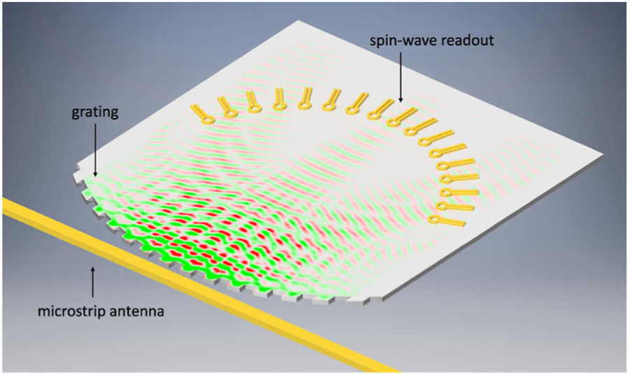
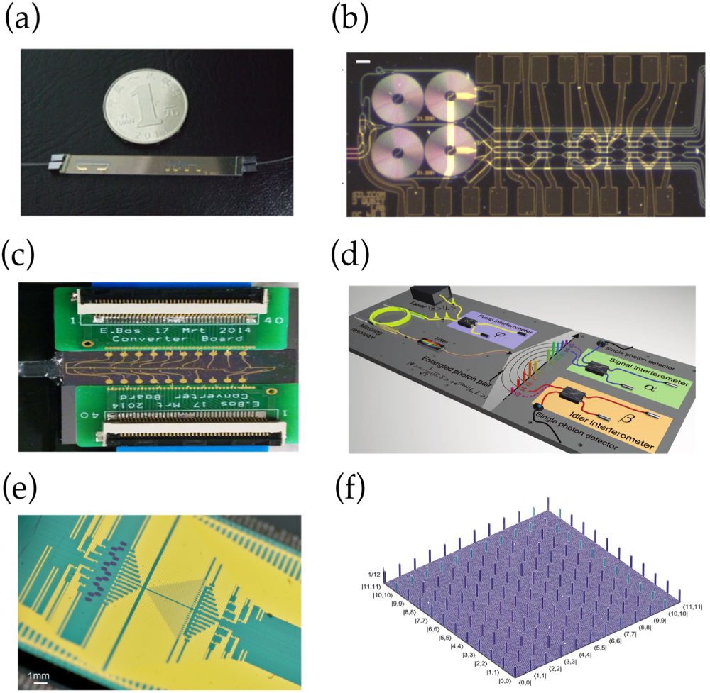
Figure 34. In linear-optics quantum computing, measurement-based heralded primitives must be multiplexed for scalability. (a) The interferometric scheme needed to produce a heralded three-photon GHZ state has not yet been demonstrated. Many such non-deterministic sources of entangled states must eventually be combined via (b) spatial, (c) spectral or (d) temporal multiplexing.
Download figure:
Standard image High-resolution image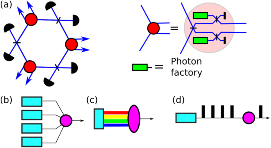
Concluding remarks
Quantum optics has a long pedigree in academic laboratories, precisely because quantum effects are easily accessible at room temperature, without the need for cryogenics, vacuum systems, advanced nanofabrication or extreme electromagnetic shielding. This gives a clue to the potential scalability of linear optical quantum computing. The technical difficulty of achieving fast, low-loss switching or quantum memory has so far put large scale all-optical QIP out of reach. But techniques to enable efficient multiplexing are emerging: once an on-demand source of heralded GHZ entangled states (or an on-demand cubic phase gate) is demonstrated, the possibility to build fault-tolerant universal linear-optical quantum computers becomes realistic.
Acknowledgments
The author acknowledges support from a Royal Society University Research Fellowship and from the EPSRC Quantum Technology Hub NQIT.