
Abstract
Silicon nanowires were successfully synthesized by a thermal evaporation method. We have observed a strong and broad emission band centered at 670 nm, which is attributed to the quantum confinement effect related to Si nanostructures embedded in the complex SiOx matrix. By fitting an experimental Raman spectrum, we confirm that the as-received wires possess crystalline silicon cores whose sizes were around 5 nm. Furthermore, the abnormal dependence of integral photoluminescence intensity on measured temperature was investigated.
Export citation and abstract BibTeX RIS

Content from this work may be used under the terms of the Creative Commons Attribution-NonCommercial-ShareAlike 3.0 licence. Any further distribution of this work must maintain attribution to the author(s) and the title of the work, journal citation and DOI.
1. Introduction
In recent years, silicon nanostructures have been extensively studied both theoretically and experimentally to realize their possible applications [1]. Silicon nanowires (Si NWs) exhibit novel chemical and physical properties due to their dimensions at the nano-scale, and offer great potential in the fields of electronics, photonics, chemical sensors and biological systems [1–9]. Current interest focuses on the band-gap expansion of Si nanocrystals compared with that of bulk materials based on the quantum confinement effect [2–4]. Si NWs with various morphologies have been fabricated using several methods, such as plasma-assisted chemical vapor deposition [3], sputtering [10] and laser ablation [11].
In this work, we report on the photoluminescence (PL) properties of the Si NWs synthesized by thermal evaporation via the vapour–liquid–solid (VLS) mechanism using Au as the catalyst. An intense red band centered at 670 nm was observed at room temperature. The PL spectra at different temperatures and the Raman scattering spectrum all support the hypothesis that the red emission band possibly originates from the Si nanocrystals (Si NCs) confined to the complex silica matrix.
2. Experimental
The vapor source in this experiment was pure silicon (99.99%) nanopowder. The p-type silicon substrates were firstly cleaned by the standard treatment. Subsequently, these substrates were deposited with 10 nm thick Au film as the catalyst by a dc sputtering technique. Then the alumina boat, which contained the silicon powder, was placed in the center of a quartz tube in the horizontal furnace. The Au-coated substrates were located evenly along the downstream side of the flowing argon. Before heating, the quartz tube was purged with high purity argon flow at a rate of 200 sccm for 30 min. Then the furnace was heated to 1200 °C and held at this temperature for 45 min while the Ar flow was kept constant at 50 sccm. The samples were then oxidized by argon and oxygen (50 sccm) gas mixture for 15 min at 300 °C in order to create a complex SiO x structure. The furnace was then cooled down to room temperature naturally.
The morphologies of as-prepared samples were examined by field emission scanning electron microscope (FESEM S4800). Raman spectra were taken by a LabRAM 1B Yvon Raman spectrometer at room temperature in backscattering configuration with a 488 nm argon laser line. PL spectra were recorded by a system consisting of a Peltier cooled CCD and a He-Cd laser (325 and 442 nm lines) as an excitation source. The samples were mounted on the cold finger of the variable temperature cryostat. The PL measurements were implemented at different temperatures from 11 to 300 K. All spectra were then corrected to the system sensitivity.
3. Results and discussion
Figure 1 shows a SEM image of as-received Si NWs, where a large quantity of NWs can be observed. The diameters of the NWs vary from 30 to 80 nm and the typical length is 400 nm. Most of the NWs are smooth and uniform along the wire axis. Some particles located on the tip of the NWs can be seen clearly. They may be Au particles formed in the catalytic processes. From this result, we believe that the growth of as-synthesized NWs was based on the VLS mechanism [10].
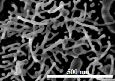
Figure 1 SEM image of Si NWs on Si substrate with Au catalyst.
Figure 2 shows a broad red emission band measured at room temperature centered on 1.9 eV (670 nm). This red spot was clearly visible to the human eye. The origin of this band is attributed to the quantum confinement effect reflecting to Si NCs embedded in the complex SiO x matrix.
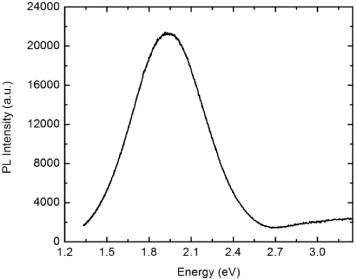
Figure 2 Room temperature photoluminescence of Si NCs embedded in SiO x matrix. The wavelength of the excitation source is 325 nm.
According to the calculations of Ding et al [12] for Si NCs embedded in SiO x , when silicon nanostructures exhibit band-gap expansion of 0.78 eV compared with that of bulk silicon (1.12 eV), the average size of Si NC should be 4.9 nm. This result is in good agreement with the calculation of the size of Si NCs based on the quantum confinement effect computed by Istam et al [13]. To confirm this observation, we have studied Raman scattering spectra of Si NWs removed from the sample (figure 3). Despite the fact that the Raman signal was very weak because of the low density of the wires, a peak at 517 cm −1 was clearly observed. This reflects the optical phonon of crystalline Si embedded in an SiO x matrix.
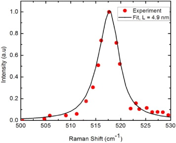
Figure 3 Raman spectrum of Si NWs taken with a 488 nm Ar laser line compared with the fitting spectrum, L=4.9 nm.
A quantitative model was developed by Richter et al [14] and was later improved by Campbell and Fauchet [15] to estimate the average size (or correlation length) L of the nanocrystals from the Raman spectrum (RS). Using this model, the first-order Raman intensity I(ω) is

where Γ is the natural line width (Γ=4 cm
−1 for c-Si at room temperature including instrumental contributions); q and L are expressed in terms of 2π/a and a, respectively, in which a=0.54 nm is the lattice constant of silicon; and ω(q) is the dispersion relation for optical phonons in c-Si. To fit the line shape, we used the analytical form ω(q)=A−Bq2, with A=518.6 cm
−1 and B=10 cm
−1, which reproduces the dispersion relation of LO phonons along the [001]-direction in Si crystals. Since LO and TO phonons are degenerate at (and very near) the Brillouin zone center and the phonons contributing to the integral are from near the zone center if L >a, this analytical dispersion should be a good approximation for L >a [14]. In figure 3, we reproduced the experimental RS data, fitted this data using equation (
We considered PL spectra at different temperatures ranging from 11 to 300 K (figure 4) using a 325 nm excitation line from a He-Cd laser. The temperature dependence of the integral PL intensities was plotted in figure 5. The emission band is broad (full-width at half-maximum around 0.48 eV), probably due to the wide distribution of nanocrystal sizes [16]. A shift of the peak position to higher energies was observed when the temperature increased to 300 K, while the overall spectral shape hardly changes. The point that the PL spectrum shape does not change, but only the position shifts higher with increasing temperature, indicates that the temperature dependence of the emission intensity is the same for all nanocrystal sizes that contribute to the spectrum.
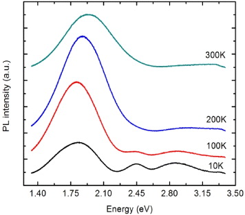
Figure 4 PL spectra of Si NWs at different temperatures.
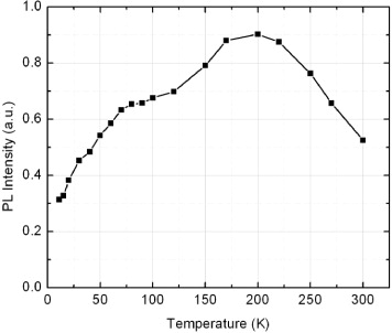
Figure 5 Temperature dependence of the photoluminescence intensity (PL) of Si NWs.
At 10 K, we see two additional emission bands with larger energies peaked at 2.45 and 2.9 eV. Their PL intensities decreased when the temperature increased. These emission bands were ascribed to oxygen vacancies or defect centers [17]. Figure 5 shows the dependence of the integral PL intensity on temperature. When the temperature increases, the peak intensity initially increases up to 200 K and subsequently decreases with higher temperatures. The origin of this dependence was explained by Brongersma et al [16] and Calcott et al [18], and calculated in detail by Duong et al [19].
4. Conclusion
In summary, we have successfully prepared the silicon nanowires by an Au-assisted thermal evaporation process via the VLS mechanism. These Si NWs exhibit intense red emission at room temperature. The shape and the peak position reveal the quantum confinement effect of the emission mechanism. The Raman spectrum was analyzed and disclosed the effective size of the silicon nanocrystal of about 5 nm. The abnormal dependence of integral PL intensity on temperature was also presented.
Acknowledgment
This work was financially supported by the National Foundation for Science and Technology Development (NAFOSTED), Vietnam, under project No. 103.02.83.09.