

Abstract
Isolating single unit-cell thin layers from the bulk matrix of layered compounds offers tremendous opportunities to design novel functional electronic materials. However, a comprehensive thickness dependence study is paramount to harness the electronic properties of such atomic foils and their stacking into synthetic heterostructures. Here we show that a dimensional crossover and quantum confinement with reducing thickness result in a striking non-monotonic evolution of the charge density wave transition temperature in VSe2. Our conclusion is drawn from a direct derivation of the local order parameter and transition temperature from the real space charge modulation amplitude imaged by scanning tunnelling microscopy. This study lifts the disagreement of previous independent transport measurements. We find that thickness can be a non-trivial tuning parameter and demonstrate the importance of considering a finite thickness range to accurately characterize its influence.
Export citation and abstract BibTeX RIS
1. Introduction
In the wake of the systematic exfoliation of graphite into one atom thin carbon sheets, an increasing number of layered compounds can now be isolated from their bulk matrix in the form of one to few unit-cell thin layers [1]. These sheets often feature unique [2–4] or enhanced [5, 6] properties in comparison to their parent bulk compounds. They depend on material thickness and can be further tuned through doping, electrostatic gating [7] and assembly of distinct layers into complex heterostructures [1, 8]. Transition metal dichalcogenides (TMDs) are of particular interest in this context. They can be readily exfoliated into thin flakes down to the single unit-cell limit [9] and offer a unique playground for studying the thickness dependence of their electronic properties. For example, in MoS2, photoactive transitions become available in the single layer limit due to the appearance of a direct gap in the band structure [10]. Metallic TMDs host a variety of electronic phases like superconductivity and charge density waves (CDW) [11–16]. Exfoliation offers a new degree of freedom to engineer these electronic ground states via the thickness of the host crystal. However, the detailed thickness dependence of their transition temperature, especially in the ultrathin limit, remains unclear [5, 6, 17–21]. Unfortunately, thin flakes of metallic TMDs often degrade in air [22, 23] and have thus been much less studied than their semiconducting and insulating counterparts. To overcome this limitation, we developed a mechanism enabling in situ exfoliation [24].
This study is focused on the thickness dependence of the CDW phase in VSe2, a metallic TMD that grows in the 1T polymorph. It consists of van der Waals bonded slabs of triangular vanadium layers sandwiched between two triangular selenium layers (figure 1(a), left inset). Each vanadium is surrounded by six selenium atoms in an octahedral configuration with in plane and out of plane lattice constants  Å and
Å and  Å, respectively [25]. Bulk 1T-VSe2 undergoes a CDW phase transition at
  K into a commensurate 4a × 4a superlattice within the layers (ab-plane) and an incommensurate
  modulation along the c-axis [25–27]. The CDW transition temperature in thin flakes (Tc) has been found to deviate up to 30% from these bulk values, with contradicting findings where Tc is either increased [18] or reduced [19], seemingly dependent on sample preparation [28].

Figure 1. Transport and STM characterization of bulk 1T-VSe2 single crystals. (a) Resistivity as a function of temperature with a kink near 105 K associated with the CDW phase transition (left inset: 1T-VSe2 crystal structure; right inset:  ). (b) Differential tunneling conductance
  and (inset)
  spectra measured at 77.6 K on the surface shown in panel (c). (c) 10 × 10 nm2 atomic resolution STM image (Vbias = −100 meV,
  = 10 pA) of a cleaved surface at 77.6 K and (d) corresponding Fourier transform. Red and green circles indicate the first-order atomic lattice and CDW modulation peaks, respectively. The circle size depicts the integration area around each peak used to calculate the CDW order parameter
  .
.
Download figure:
Standard image High-resolution image2. Results and discussion
Before investigating the thickness dependence of the CDW, we have characterized it in bulk single crystals by transport measurements and scanning tunnelling microscopy (STM). Resistivity as a function of temperature (figure 1(a)) shows a characteristic kink at the CDW phase transition  K, in agreement with previous studies [29]. Constant current STM images and corresponding Fourier transforms at 77.6 K (figures 1(c) and (d)) clearly reveal a triangular atomic lattice (
 Å) and the in plane
  commensurate CDW modulation [30]. Tunneling spectroscopy (figure 1(b)) is consistent with data reported elsewhere [31], including a characteristic conductance peak associated with the vanadium derived
  -band below the Fermi level (
 ) and an asymmetric
  -shaped background centered on
  . These prominent spectral features do not change up to room temperature [31], except for thermal broadening. They also remain essentially unchanged on all the exfoliated flakes discussed here.
To gain insight into the thickness dependence of the CDW, we take advantage of steps and terraces naturally present on the exfoliated flakes. The flake thickness is directly determined by STM from a topographic line profile between the reconstructed Au(1 1 1) and the top of the investigated exfoliated terrace. Both surfaces are atomically flat, thus enabling the local thickness to be determined in principle with single layer accuracy, especially in the thinnest regions along the edges of the flakes. The uncertainty on the flake thickness is thus less than the symbol size in figures 3 and 4. Here, we concentrate on STM micrographs measured above 77 K, near  where thickness dependent CDW features are most prominent. Topographic and CDW features imaged by STM on different exfoliated thin flakes and terraces with distinct thicknesses (figure 2) are very similar to those in bulk crystals. Remarkably, we observe the same
  charge order down to the thinnest sample studied (2.2 nm). However, a closer inspection of the 77.6 K micrographs reveals a noticeably weaker CDW amplitude in the 20 nm thin region than in all other thicknesses. At 95.0 K, closer to
  , the CDW is almost completely suppressed on the 20 nm and 50 nm thin flakes—similar to what we observe in bulk crystals—while it remains surprisingly strong on the thinnest 10 nm flake.

Figure 2. STM images of exfoliated 1T-VSe2 flakes. 5 × 5 nm2 atomic resolution micrographs (Vbias  −100 meV,
  = 10 pA) measured on different thickness terraces and flakes at 77.6 K and 95.0 K. The atomic lattice is well resolved in all images. The CDW is strongest in the thinnest regions (10 nm) at both temperatures and nearly absent in the 20 nm and 50 nm thin regions at 95.0 K.
Download figure:
Standard image High-resolution image
Figure 3. Temperature and thickness dependencies of the CDW order parameter  in 1
in 1 -VSe2 extracted from topographic STM images. (a)
  as a function of temperature in a bulk single crystal near the phase transition. The solid line is a fit to the BCS approximate form
  , where
  105 K and the only fitting parameter is determined to be
  . (b)
. (b)  as a function of temperature for three different thicknesses. The solid lines are calculated with the above BCS interpolation using the bulk scaling factor A and the local Tc calculated from
  for each thickness. (c)
  as a function of thickness at 77.6 K. In all panels the error bars correspond to the dispersion of
  as determined by analyzing many different STM images for a given temperature and thickness. (d) 3D representation of the dimensional crossover from 3D to 2D behavior.
Download figure:
Standard image High-resolution image
Figure 4. Thickness dependence of the CDW transition temperature  in 1
in 1 -VSe2. Solid squares represent Tc calculated from the charge modulation amplitude imaged by STM using equations (1) and (2). They reveal a clear non-monotonic dependence of Tc on crystal thickness. The vertical error bars correspond to the dispersion from many different STM images. The green dashed line symbolizes the transition temperature of a bulk sample. Our data are in quantitative agreement with and reconcile data from previous transport experiments covering separate thickness ranges (represented by the solid red circle [18] and the solid blue line [19]).
Download figure:
Standard image High-resolution image
A more quantitative analysis of the CDW contrast revealed by STM is required to go beyond the above approximate visual assessment. The amplitude of the gap near  associated with the CDW phase transition would be a natural order parameter. However, there is no consensus on the CDW gap measured by scanning tunneling spectroscopy in VSe2, with reported amplitudes ranging from 80 mV and 40 mV to no visible gap feature [30–32]. The vanadium derived d-band obscures the CDW gap and tunneling spectroscopy does not show any significant reduction in the LDOS at
  at the phase transition (figure 1(b)). This observation is consistent with the tiny portion of the Fermi surface (FS) that is gaped in the CDW phase of 1T-VSe2 [33], making it impractical to identify the phase transition by the opening of the gap.
A convenient alternative measure to describe the phase transition when the quasi-particle gap is not clearly observable is the CDW modulation amplitude [34], which depends linearly on the gap in a mean field description [35]. For a quantitative analysis of the CDW phase transition, we thus introduce an order parameter  defined as
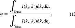
where  is the amplitude in Fourier space and
  and
and  are circular shaped integration areas around the CDW and lattice peaks, respectively (figure 1(d)).
  and
and  were chosen such that the k-space area is the same for all examined micrographs (
 ). We normalize to the atomic lattice components to account for possible differences in tunneling conditions, which result in small variations in the appearance of the CDW patterns imaged by STM. Note this variability is the same for bulk crystals and thin exfoliated flakes and does not affect the calculated order parameter
  .
.
The temperature dependence of  near the phase transition of a single crystal (figure 3(a)) can be modeled in a mean field description by a phenomenological BCS gap equation [36]:

where  is a scaling factor to be determined. The solid line in figure 3(a) is a fit of equation (2) to the experimental data points, where we have set
  . The fit has a single adjustable parameter which we find to be
 . The consistent picture emerging from this analysis confirms that equation (1) is an adequate measure of the order parameter enabling a quantitative analysis of the CDW phase transition. Examining a large set of STM images from different terraces and flakes at
  K, we find a non-monotonic thickness dependence of the CDW order parameter (figure 3(c)).
  is gradually decreasing from its bulk value when reducing the thickness in thicker flakes. This thickness dependence is reversed in the thinner flakes below 20 nm, with
  increasing to even significantly exceed the bulk value in the thinnest regions measured here (2.2 nm). Defects have been shown to stabilize a finite CDW amplitude above Tc in their vicinity [37]. However, we can exclude this scenario for the enhanced phase transition in the thinnest flakes because Tc is determined from data measured at 77.8 K and averaged over many different STM images with few defects.
The order parameter  is not suitable for a direct comparison of our STM data with published transport experiments [18, 19]. The latter report
  as a function of thickness, which is challenging to measure by STM because of thermal drift making it difficult to maintain the tip position over a specific location while changing the temperature above 77 K. As it turns out, we can use equation (2) to calculate the local
  based on
  extracted from STM images at a given temperature
  . Assuming the scaling factor A is the same for all thicknesses, equation (2) provides a direct correspondence between
  and the order parameter
  . To verify this assumption, we plot equation (2) for the 10 nm, 20 nm, and 50 nm thin terraces, using the transition temperature
  = 122 K, 87 K, and 100 K, respectively, calculated for each thickness from
  . The agreement with the experimental data points is excellent as shown in figure 3(b).
This demonstrates the validity of this method, providing an unprecedented ability to determine the local CDW transition temperature solely based on the charge modulation amplitude measured by STM. The expected CDW gap amplitudes within this weak coupling model are in the range of 3.8 meV–5.7 meV depending on crystal thickness, too small to be properly resolved above 77 K by tunneling spectroscopy.
The CDW transition temperature calculated for different thicknesses using the above method are plotted in figure 4. They are in remarkable quantitative agreement with independent transport studies [18, 19]. The most striking findings of our analysis are a non-monotonic thickness dependence of  and a significant increase of
  above the bulk value in the thinnest terraces. The opposite thickness dependencies of
  we find in very thin compared to thicker terraces reconcile the contradicting results reported by Xu et al [18] and Yang et al [19]. That disagreement has been blamed on the distinct liquid and mechanical exfoliation techniques used in these studies, when it is in fact the result of investigating different thickness ranges. The STM data presented in figure 4 suffers no such ambiguity; they were obtained with the same tip probe on flakes prepared in an identical mechanical exfoliation process.
The two distinct and opposite thickness dependencies of the CDW transition temperature illustrated in figures 3(c) and 4 suggest a crossover from a three-dimensional (3D) regime in bulk and thick flakes to a two-dimensional (2D) regime in the thinner flakes.  has been found to increase with decreasing thickness also for other very thin TMD compounds [5, 6]. However, these studies lack important real space information to fully assess the nature of the CDW. STM directly and unambiguously shows no alteration in the CDW symmetry and periodicity with thickness and temperature. The only modification we observe is the charge modulation amplitude associated with a modified Tc. We propose that the enhanced Tc in the thinnest samples is a consequence of spatial confinement, in analogy to BCS superconductors governed by a gap equation similar to equation (2). In that case, for a confinement potential
  above a critical value, theory predicts the superconducting transition temperature (
 ) to increase with decreasing thickness before vanishing to zero in the zero thickness limit [38]. The characteristic thickness
  for which
  is maximum in this model depends on
  , on the coupling strength, and on the carrier density. It is important to note that
  does not necessarily correspond to the single layer limit. It can be larger and it is thus crucial to examine a range of thicknesses to draw definite conclusions about the thickness dependence of Tc. In particular, considering only bulk and single layer crystals may lead to inaccurate conclusions about the effect of dimensional confinement, even in the same material if different preparation and substrates result in different
  .
.
The decreasing Tc with decreasing thickness in thick flakes can be understood considering the FS topology of VSe2. It has a significant dispersion of a few eV along  [27, 33], different from the mostly 2D FS of other layered TMDs. Photoemission [27, 39] reveals large parallel FS portions centered at the M(L) points of the Brillouin zone. They offer good in-plane nesting conditions that persist for all
  . This nesting is strongest at a particular
  , resulting in an effective out of plane nesting vector and a 3D CDW [27] in bulk VSe2. Upon thinning the bulk crystal, the out-of-plane nesting condition eventually becomes weaker due to the discretization of the FS by the reduced number of available
  points. This drives the system into a weaker 2D charge order that is further suppressed by enhanced fluctuations expected in 2D. This second regime becomes dominant above a critical thickness beyond which it will obscure the hallmarks of quantum confinement that defines the behavior in the thinnest flakes.
3. Conclusion
In summary, we find a striking non-monotonic thickness dependence of the CDW transition temperature in mechanically exfoliated 1T-VSe2 from bulk to 2.2 nm thin flakes. On the other hand, the modulation period and alignment with the atomic lattice are entirely independent on thickness. We propose this behavior is a consequence of a 3D to 2D dimensional crossover in the FS topology around 20 nm thickness combined with quantum confinement in thinner flakes. The dimensional crossover weakens the bulk CDW in the thicker flakes and the confinement enhances it in the thinner ones (figure 3(d)). Unambiguous evidence for this behavior is provided by the local  determined from the CDW order parameter measured by STM over an unprecedented broad range of thicknesses for a single experiment. We demonstrate that the charge modulation amplitude provides a suitable measure of the CDW phase transition order parameter. This allows a robust determination of the local critical temperature based solely on STM topographic images of the CDW at a given temperature below
  . Interestingly, the exact same approximate form of the (weak coupling) BCS equation quantitatively describes the CDW order parameter and critical temperature, independent of sample thickness and temperature. The present study thus strongly suggests that the thickness dependence reported here is not a consequence of a varying coupling strength or the signature of a different CDW phase, but indeed due to the FS topology, dimensional crossover and quantum confinement.
4. Methods
1T-VSe2 single crystals were grown by chemical vapor transport using I2 as a transport agent and then mechanically exfoliated in situ (3 · 10−8 mbar) onto Au(1 1 1) single crystal substrates. Prior to the exfoliation, the Au(1 1 1) surface was cleaned and reconstructed by repeated cycles of Ar+ ion sputtering and annealing at 450 °C in ultra-high vacuum (UHV). The exfoliated flakes are hardly visible by optical means in our UHV scanning tunneling microscope (STM) setup. We thus relied on a suitable coverage density produced by our bespoke in situ exfoliation mechanism [24] to position the STM tip over an exfoliated flake in a systematic scan and search procedure. The STM experiments were done in UHV (base pressure 2 · 10−10 mbar) using tips electrochemically etched from an annealed tungsten wire. The bias voltage was applied to the sample. Tunneling  and differential conductance
  spectra were acquired simultaneously using a standard lock-in technique with a 7.1 mV rms bias modulation at 337.7 Hz.
Acknowledgment
We acknowledge A Morpurgo, Ch Berthod and T Giamarchi for stimulating discussions, L Musy for his contributions to the initial attempts of in situ exfoliation, and G Manfrini and A Guipet for their technical assistance. This project was supported by the Swiss National Science Foundation through Sinergia project (grant 147607).
Author contributions
CR conceived the experiments. ÁP and AS designed and carried out the experiments. CB and EG synthesized the bulk crystals and measured their resistivity. ÁP analyzed the STM data. ÁP, AS and CR discussed the data and wrote the text. All authors contributed to the manuscript revisions.
The authors declare no competing financial interests. Recent low temperature STS measurements of the CDW gap [40] give consistent results with the expected values from our analysis.