
Abstract
We present an overview of the main techniques for production and processing of graphene and related materials (GRMs), as well as the key characterization procedures. We adopt a 'hands-on' approach, providing practical details and procedures as derived from literature as well as from the authors' experience, in order to enable the reader to reproduce the results.
Section I is devoted to 'bottom up' approaches, whereby individual constituents are pieced together into more complex structures. We consider graphene nanoribbons (GNRs) produced either by solution processing or by on-surface synthesis in ultra high vacuum (UHV), as well carbon nanomembranes (CNM). Production of a variety of GNRs with tailored band gaps and edge shapes is now possible. CNMs can be tuned in terms of porosity, crystallinity and electronic behaviour.
Section II covers 'top down' techniques. These rely on breaking down of a layered precursor, in the graphene case usually natural crystals like graphite or artificially synthesized materials, such as highly oriented pyrolythic graphite, monolayers or few layers (FL) flakes. The main focus of this section is on various exfoliation techniques in a liquid media, either intercalation or liquid phase exfoliation (LPE). The choice of precursor, exfoliation method, medium as well as the control of parameters such as time or temperature are crucial. A definite choice of parameters and conditions yields a particular material with specific properties that makes it more suitable for a targeted application. We cover protocols for the graphitic precursors to graphene oxide (GO). This is an important material for a range of applications in biomedicine, energy storage, nanocomposites, etc. Hummers' and modified Hummers' methods are used to make GO that subsequently can be reduced to obtain reduced graphene oxide (RGO) with a variety of strategies. GO flakes are also employed to prepare three-dimensional (3d) low density structures, such as sponges, foams, hydro- or aerogels. The assembly of flakes into 3d structures can provide improved mechanical properties. Aerogels with a highly open structure, with interconnected hierarchical pores, can enhance the accessibility to the whole surface area, as relevant for a number of applications, such as energy storage. The main recipes to yield graphite intercalation compounds (GICs) are also discussed. GICs are suitable precursors for covalent functionalization of graphene, but can also be used for the synthesis of uncharged graphene in solution. Degradation of the molecules intercalated in GICs can be triggered by high temperature treatment or microwave irradiation, creating a gas pressure surge in graphite and exfoliation. Electrochemical exfoliation by applying a voltage in an electrolyte to a graphite electrode can be tuned by varying precursors, electrolytes and potential. Graphite electrodes can be either negatively or positively intercalated to obtain GICs that are subsequently exfoliated. We also discuss the materials that can be amenable to exfoliation, by employing a theoretical data-mining approach.
The exfoliation of LMs usually results in a heterogeneous dispersion of flakes with different lateral size and thickness. This is a critical bottleneck for applications, and hinders the full exploitation of GRMs produced by solution processing. The establishment of procedures to control the morphological properties of exfoliated GRMs, which also need to be industrially scalable, is one of the key needs. Section III deals with the processing of flakes. (Ultra)centrifugation techniques have thus far been the most investigated to sort GRMs following ultrasonication, shear mixing, ball milling, microfluidization, and wet-jet milling. It allows sorting by size and thickness. Inks formulated from GRM dispersions can be printed using a number of processes, from inkjet to screen printing. Each technique has specific rheological requirements, as well as geometrical constraints. The solvent choice is critical, not only for the GRM stability, but also in terms of optimizing printing on different substrates, such as glass, Si, plastic, paper, etc, all with different surface energies. Chemical modifications of such substrates is also a key step.
Sections IV–VII are devoted to the growth of GRMs on various substrates and their processing after growth to place them on the surface of choice for specific applications. The substrate for graphene growth is a key determinant of the nature and quality of the resultant film. The lattice mismatch between graphene and substrate influences the resulting crystallinity. Growth on insulators, such as SiO2, typically results in films with small crystallites, whereas growth on the close-packed surfaces of metals yields highly crystalline films. Section IV outlines the growth of graphene on SiC substrates. This satisfies the requirements for electronic applications, with well-defined graphene-substrate interface, low trapped impurities and no need for transfer. It also allows graphene structures and devices to be measured directly on the growth substrate. The flatness of the substrate results in graphene with minimal strain and ripples on large areas, allowing spectroscopies and surface science to be performed. We also discuss the surface engineering by intercalation of the resulting graphene, its integration with Si-wafers and the production of nanostructures with the desired shape, with no need for patterning.
Section V deals with chemical vapour deposition (CVD) onto various transition metals and on insulators. Growth on Ni results in graphitized polycrystalline films. While the thickness of these films can be optimized by controlling the deposition parameters, such as the type of hydrocarbon precursor and temperature, it is difficult to attain single layer graphene (SLG) across large areas, owing to the simultaneous nucleation/growth and solution/precipitation mechanisms. The differing characteristics of polycrystalline Ni films facilitate the growth of graphitic layers at different rates, resulting in regions with differing numbers of graphitic layers. High-quality films can be grown on Cu. Cu is available in a variety of shapes and forms, such as foils, bulks, foams, thin films on other materials and powders, making it attractive for industrial production of large area graphene films. The push to use CVD graphene in applications has also triggered a research line for the direct growth on insulators. The quality of the resulting films is lower than possible to date on metals, but enough, in terms of transmittance and resistivity, for many applications as described in section V.
Transfer technologies are the focus of section VI. CVD synthesis of graphene on metals and bottom up molecular approaches require SLG to be transferred to the final target substrates. To have technological impact, the advances in production of high-quality large-area CVD graphene must be commensurate with those on transfer and placement on the final substrates. This is a prerequisite for most applications, such as touch panels, anticorrosion coatings, transparent electrodes and gas sensors etc. New strategies have improved the transferred graphene quality, making CVD graphene a feasible option for CMOS foundries. Methods based on complete etching of the metal substrate in suitable etchants, typically iron chloride, ammonium persulfate, or hydrogen chloride although reliable, are time- and resource-consuming, with damage to graphene and production of metal and etchant residues. Electrochemical delamination in a low-concentration aqueous solution is an alternative. In this case metallic substrates can be reused. Dry transfer is less detrimental for the SLG quality, enabling a deterministic transfer.
There is a large range of layered materials (LMs) beyond graphite. Only few of them have been already exfoliated and fully characterized. Section VII deals with the growth of some of these materials. Amongst them, h-BN, transition metal tri- and di-chalcogenides are of paramount importance. The growth of h-BN is at present considered essential for the development of graphene in (opto) electronic applications, as h-BN is ideal as capping layer or substrate. The interesting optical and electronic properties of TMDs also require the development of scalable methods for their production. Large scale growth using chemical/physical vapour deposition or thermal assisted conversion has been thus far limited to a small set, such as h-BN or some TMDs. Heterostructures could also be directly grown.
Section VIII discusses advances in GRM functionalization. A broad range of organic molecules can be anchored to the sp2 basal plane by reductive functionalization. Negatively charged graphene can be prepared in liquid phase (e.g. via intercalation chemistry or electrochemically) and can react with electrophiles. This can be achieved both in dispersion or on substrate. The functional groups of GO can be further derivatized. Graphene can also be noncovalently functionalized, in particular with polycyclic aromatic hydrocarbons that assemble on the sp2 carbon network by π–π stacking. In the liquid phase, this can enhance the colloidal stability of SLG/FLG. Approaches to achieve noncovalent on-substrate functionalization are also discussed, which can chemically dope graphene. Research efforts to derivatize CNMs are also summarized, as well as novel routes to selectively address defect sites. In dispersion, edges are the most dominant defects and can be covalently modified. This enhances colloidal stability without modifying the graphene basal plane. Basal plane point defects can also be modified, passivated and healed in ultra-high vacuum. The decoration of graphene with metal nanoparticles (NPs) has also received considerable attention, as it allows to exploit synergistic effects between NPs and graphene. Decoration can be either achieved chemically or in the gas phase. All LMs, can be functionalized and we summarize emerging approaches to covalently and noncovalently functionalize MoS2 both in the liquid and on substrate.
Section IX describes some of the most popular characterization techniques, ranging from optical detection to the measurement of the electronic structure. Microscopies play an important role, although macroscopic techniques are also used for the measurement of the properties of these materials and their devices. Raman spectroscopy is paramount for GRMs, while PL is more adequate for non-graphene LMs (see section IX.2). Liquid based methods result in flakes with different thicknesses and dimensions. The qualification of size and thickness can be achieved using imaging techniques, like scanning probe microscopy (SPM) or transmission electron microscopy (TEM) or spectroscopic techniques. Optical microscopy enables the detection of flakes on suitable surfaces as well as the measurement of optical properties. Characterization of exfoliated materials is essential to improve the GRM metrology for applications and quality control. For grown GRMs, SPM can be used to probe morphological properties, as well as to study growth mechanisms and quality of transfer. More generally, SPM combined with smart measurement protocols in various modes allows one to get obtain information on mechanical properties, surface potential, work functions, electrical properties, or effectiveness of functionalization. Some of the techniques described are suitable for 'in situ' characterization, and can be hosted within the growth chambers. If the diagnosis is made 'ex situ', consideration should be given to the preparation of the samples to avoid contamination. Occasionally cleaning methods have to be used prior to measurement.
Export citation and abstract BibTeX RIS

Original content from this work may be used under the terms of the Creative Commons Attribution 3.0 licence. Any further distribution of this work must maintain attribution to the author(s) and the title of the work, journal citation and DOI.
List of acronyms
| 0d | Zero dimensional |
| 1d | One dimensional |
| 1L | One layer |
| 1LG | 1 layer graphene |
| 2D | 2D Raman peak of graphene |
| 2d | Two dimensional |
| 2LG | 2 layer graphene |
| 3d | Three dimensional |
| 3LG | 3 layer graphene |
| 4LG | 4 layer graphene |
| AES | Auger electron spectroscopy |
| AFM | Atomic force microscopy |
| AGNR | GNRs with armchair edges |
| ALD | Atomic layer deposition |
| APCVD | Atmospheric pressure CVD |
| APS | Ammonium persulfate |
| ARGO | Reduced graphene oxide-based aerogels |
| ARPES | Angle resolved photoemission spectroscopy |
| BHJ | Bulk hetro junction |
| Bipy | 2,2'-Bipyridine |
| BL | Buffer layer |
| BLG | Bilayer graphene |
| BODIPY | 2,6-diiodo-1,3,5,7-tetramethyl-8-phenyl-4,4-difluoroboradiazaindacene |
| BP | Black phosphorus |
| BP3 | 3-(Biphenyl-4-yl)propane-1-thiol |
| BPT | 1,1'-biphenyl-4-thiol |
| BZ | Brillouin zone |
| Bz | Benzidine |
| CA | Cellulose acetate |
| CCS | Confinement controlled sublimation |
| c-CVD | Catalytical-chemical vapor deposition |
| CE | Counter electrode |
| CES | Constant energy surface |
| CHP | N-cyclohexyl-2-pyrrolidone |
| CL | Cathode luminiscence |
| CMC | Critical micelle concentration |
| CMOS | Complementary metal-oxide semiconductor |
| CMP | Conjugated microporous polymers |
| CNF | Carbon nanofibre |
| CNM | Carbon nanomembrane |
| CNT | Carbon nanotube |
| COD | 1,5-cyclooctadiene |
| CPD | Critical point drying |
| CTAB | Cetyl trimethyl ammonium bromide |
| CVD | Chemical vapour deposition |
| D | D Raman peak |
| DA | Diels-Alder |
| DAP | Donor–acceptor pairs |
| db | Dangling bonds |
| DBT | 4-docosyloxy-benzenediazonium tetrafluoroborate |
| DCM | Dichloromethane |
| DEA | Dissociative electron attachment |
| DES | Diethyl sulphide |
| DFT | Density functional theory |
| DGM | Density gradient medium |
| DGU | Density gradient ultracentrifugation |
| Dh | Decahedral |
| DI | Deionized water |
| DIC | Differential interference contrast |
| DMAc | N,N'-dimethylacetamide |
| DME | 1,2-dimethoxyethane |
| DMF | Dimethylformamide |
| DMSO | Dimethylsulfoxide |
| DOS | Density of states |
| DOTA | 1,4,7,10-tetraazacyclododecane-1,4,7,10-tetraacetic acid |
| DSSC | Dye-sensitized solar cell |
| EA | Elemental analysis |
| EBSD | Electron back scattering diffraction |
| EC | Ethyl cellulose |
| EDA | Ethylene-diamine |
| EE | Electrochemical exfoliation |
| EEG | Electrochemically exfoliated graphene |
| EG | Epitaxial graphene |
| EVA | Ethylene vinyl acetate |
| FCC | Face-centered cubic |
| FESEM | Field emission scanning electron microscope |
| FET | Field effect transistor |
| FIB | Focused ion beam |
| FL | Few layer |
| FLaT | Functional layer transfer |
| FLG | Few layer graphene |
| FoM | Figure of merit |
| FS | Fermi surface |
| FTIR | Fourier transform infrared spectroscopy |
| FWHM | Full width at half maximum |
| G | G Raman peak |
| G3DCN | Graphene-based covalent networks |
| GANF | Grupo Antolin nanofibres |
| GFactor | Gauge factor |
| GF | Graphene foam |
| GIC | Graphite intercalation compound |
| GnP | Graphene nanoplatelets |
| GNR | Graphene nanoribbons, nanometer wide graphene strips exhibiting a bandgap |
| GO | Graphene oxide |
| GOS | Graphene on silicon |
| GRM | Graphene and related material |
| GRMs | Graphene and related materials |
| HAADF | High angle annular dark field |
| HATU | O-(7-Azabenzotriazole-1-yl)-N,N,N,N'-tetramethyluronium hexafluorophosphate |
| HBC | Hexabenzocoronene |
| HBC-Br | 2-Bromo-11-(1'-[4'-(S-Acetylthiomethyl)phenyl]acetyl)-5,8,14,17-tetra(3',7'-dimethyloctyl)-hexa-peri-hexabenzocoronene |
| HBC-CN | 2-Cyano-11-(1'-[4'-(S-Acetylthiomethyl)phenyl]acetyl)-5,8,14,17-tetra(3',7'-dimethyloctyl)-hexa-peri-hexabenzocoronene |
| HIM | Helium ion microscope |
| hMDM | Human monocyte macrophages |
| HMDS | Hexamethyldisilazane |
| HOPG | Highly oriented pyrolytic graphite |
| HPB | S,S'-(3',4',5',6'-tetraphenyl-[1,1':2',1''-terphenyl]-4,4''-diyl) diethanethioate |
| HPL | Hot-press lamination |
| HREM | High resolution electron microscopy |
| HRP | Horseradish peroxidase |
| HRTEM | High resolution transmission electron microscopy |
| ICS | Ion cluster source |
| IFM | Inverted floating method |
| Ih | Icosahedral |
| IPA | Isopropyl alcohol |
| JCNM | Janus carbon nanomembrane |
| KPM | Kelvin probe microscopy |
| LCC | Liquid cascade centrifugation |
| LEED | Low energy electron diffraction |
| LEEM | Low energy electron microscopy |
| LIB | Lithium ion battery |
| LM | Layered material |
| LMH | Layered material heterostructure |
| LMs | Layered materials |
| LPCVD | Low pressure CVD |
| LPE | Liquid phase exfoliation |
| LRI | Liquid resin infusion |
| µ | Carrier mobilities |
| µ-ARPE | Micro spot ARPES |
| MALDI-TOF | Matrix-assisted laser desorption/ionization-time of flight |
| MBE | Molecular beam epitaxy |
| MC | Mechanically-cleaved |
| MEG | Multilayer epitaxial graphene |
| MEP | Minimum energy path |
| MICS | Multiple ion cluster source |
| mIPM | Murine intraperitoneal macrophages |
| ML | Monolayer |
| MLG | Multilayer graphene |
| MNP | Metal nanoparticle |
| MOCVD | Metalorganic chemical vapour deposition |
| MP | Moire pattern |
| MS | Mass spectrometry |
| MSCs | Micro super capacitors |
| MW | Microwave |
| MW | Molecular weight |
| N | Number of layers |
| NaCMC | Sodium carboxymethylcellulose |
| NBE | Near band edge |
| n-BuLi | n-butyllithium |
| NC | Nitrocellulose |
| Nc-AFM | Non-contact atomic force microscopy |
| NDI | Naphthalene diimide |
| NMP | N-methyl-2-pyrrolidone |
| NMR | Nuclear magnetic resonance |
| NP | Nanoparticle |
| NPTH | Naphtalene-2-thiol |
| ODCB | 1,2-dichlorobenzene |
| OPV | Organic photovoltaics |
| ORR | Oxygen reduction reaction |
| Otf | Trifluoromethanesulfonate |
| OTFT | Organic thin film transistor |
| P3HT | Poly(3-hexylthiophene) |
| PAH | Polycyclic aromatic hydrocarbon |
| PANi | Polyaniline |
| PCBM | Phenyl-C61-butyric acid methyl ester |
| PDI | Perylene diimide |
| PDMS | Polydimethylsiloxane |
| PE | Polyethylene |
| PECVD | Plasma enhanced chemical vapour deposition |
| PEDOT | Poly(3,4 ethylenedioxythiophene) |
| PET | Polyethylene terephthalate |
| PhCN | Benzonitrile |
| PI | Polyimide |
| PL | Photoluminescence |
| PMMA | Poly(methyl methacrylate) |
| PPF | Pyrolyzed photoresist film |
| PPP | Polu(p -phenylene) |
| PS | Polystyrene |
| PTCVD | Photo thermal CVD |
| PTFE | Polytetrafluoroethylene |
| PVA | Polyvinyl acetate |
| PVC | Polyvinyl chloride |
| PVDF | Polyvinylidene difluoride |
| PVP | Polyvinylpyrrolidone |
| PVT | Physical vapor transport |
| QFBLG | Quasi free-standing bilayer graphene |
| QFSLG | Quasi free-standing single layer graphene |
| r-(ECR-CVD) | Remote electron cyclotron resonance plasma assisted chemical vapor deposition |
| RBLM | Radial-breathing-like mode |
| RCA1, RCA2 | Standard sets of wafer cleaning steps which need to be performed before high-temperature processing steps |
| RE | Reference electrode |
| RF | Radiofrequency |
| RF-ID | Radio-frequency identification |
| RGO | Reduced graphene oxide |
| RHEED | Reflection high energy electron diffraction |
| RIE | Reactive ion etching |
| Rpm | Revolutions per minute |
| RT | Room temperature |
| RTM | Resin transfer moulding |
| RTP | Rapid thermal process |
| RZC | Rate zonal centrifugation |
| SAED | Selected area electron diffraction |
| SAM | Self-assembled monolayer |
| SARPES | Spin resolved ARPES |
| SAV | Single atom vacancies |
| SBS | Sedimentation based separation |
| SC | Sodium cholate |
| SDBS | Sodium dodecyl benzene sulfonate |
| SDC | Sodium deoxycholate |
| SDS | Sodium dodecyl sulfate |
| SEC | Size exclusion chromatography |
| SEM | Scanning electron microscopy |
| SET | Single electron transfer |
| SL | Single-layer |
| SLG | Single layer graphene |
| Slm | Standard liter per minute |
| SOI | Silicon on insulator |
| STEM | Scanning transmission electron microscopy |
| SThM | Scanning thermal microscopy |
| STM | Scanning tunnelling microscopy |
| STS | Scanning tunnelling spectroscopy |
| SuMBE | Supersonic molecular beam epitaxy |
| SWCNT | Single wall carbon nanotube |
| T | Temperature |
| TAC | Thermally assisted conversion |
| Tb | Temperature of the bubbler |
| TCB | 1,2,4-trichlorobenzene |
| TCF | Transparent conducting film |
| TCNQ | Tetracyanoquinodimethane |
| TEM | Transmission electron microscopy |
| TEMPO | 2,2,6,6-tetramethyl-1-piperidinyloxy |
| TGA | Thermogravimetric analysis |
| THF | Tetrahydrofuran |
| THz-TDS | THz-time domain spectroscopy |
| TLG | Trilayer graphene |
| TMC | Transition metal chalcogenide |
| TMD | Transition metal dichalcogenide |
| TOA | Tetraoctylammonium |
| TPT | [1'',4',1',1]-Terphenyl-4-thiol |
| Tr-ARPES | Time-resolved ARPES |
| TRT | Thermal release tape |
| UHV | Ultra high vacuum |
| ULF | Ultra low frequency |
| UV | Ultraviolet |
| UVA | Ultraviolet adhesive |
| Uv–Vis | Ultraviolet–visible |
| vdW | van der Waals |
| VPE | Vapour phase epitaxy |
| WE | Working electrode |
| XPS | X-ray photoelectron spectroscopy |
| Z | Reciprocal of the Ohnesorge number |
| ZGNR | GNRs with zigzag edges |
I. Bottom-up
I.1. Graphene nanoribbons
GNRs are an interesting family of materials combining aspect ratios allowing to bridge the range of (sub-) nanometer dimensions with ultimate structure-properties relationship (GNR width, below 5 nm) and mesoscopic dimensions (GNR length up to 500 nm). This makes GNRs accessible to established top-down contacting strategies and thus allows their device integration. For GNRs with armchair edges (AGNRs), theory predicts the opening of sizable bandgaps as soon as their widths falls below ~2 nm [1–5]. This is due to quantum confinement and edge effects and can qualitatively be understood by slicing the graphene Dirac cone along k-lines in the reciprocal space that are compatible with the hard-wall boundary conditions set by the finite AGNR width. The further these cuts of allowed electronic states are away from the K point of the Brillouin zone of graphene, the larger is their bandgap [6]. AGRNs were predicted to show metallic to semiconducting behavior, depending on their width [2, 7–9]. Generally, AGRNs exhibiting widths smaller than 10 nm behave as semiconductors with non-zero bandgaps that increase as the they become narrower [5, 7–11]. E.g., AGNRs as narrow as 2–3 nm are expected to havea bandgap ~0.7 eV, which is comparable to that of Ge [5]. In contrast, early theoretical studies indicated that zigzag GNRs, ZGNRs, have metallic properties with zero bandgap irrespective of the width, showing strongly localized edge states at the zigzag sites [7], with ferromagnetic coupling along and antiferromagnetic coupling across the edges [12]. Spin-polarized density functional theory DFT calculations have found that AGNRs are always semiconductors and that the ground state of ZGNRs has an antiferromagnetic configuration, where electronic states with opposite spins are highly localized at the two ZGNR edges and are responsible for the opening of a gap [1712, 1713]. Thus, small differences in width and edge configuration lead to large variations in GNR properties [5, 10, 11], making it imperative to control the GNR structure on the atomic level to achieve the desired (opto)electronic and magnetic properties with high accuracy and reproducibility. While this is beyond the level of what can be currently controlled by top-down structuring methods, such as lithographic patterning [13–16] or cutting of CNTs[17–20], advances in bottom-up fabrication have shown that GNRs with specific edge structure and width are accessible [21]. Not only purely A or ZGNRs can be synthesized. Other types in between named chevron- or necklace-type can be designed and prepared as well [1724].
I.1.1. Solution synthesis of GNRs
The concept of solution based bottom-up synthesis relies on the preparation of large polycyclic aromatic hydrocarbons (PAHs), often referred to as nanographenes [22, 23] The reaction is based on the intramolecular oxidative cyclodehydrogenation of corresponding oligophenylene precursors and was extended from defined molecules to polymers, i.e. from PAHs to GNRs [23]. Since then, the synthesis of GNRs through intramolecular cyclodehydrogenation of polyphenylene polymers was achieved, through AA-, AB- and A2B2-type polymerizations as summarized in Refs. [24–27].
The most critical issue in the solution-synthesis is to achieve high (>600 000 g mol−1 on average by Diels Alder (DA) polymerization) molecular weight of the precursor polymer. While the width of GNRs is determined by the monomer dimensions, the molecular weight is directly proportional to the number of repeating units, therefore proportional to the length of the resulting GNR after the cyclodehydrogenation -graphitization- step. E.g. DA polymerization provides a molecular weight >600 000, on average corresponding to a length of 600 nm [23].
Figure I.1 provides an overview of the polymerization routes explained in what follows along with the relevant references.
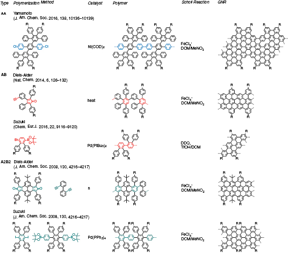
Figure I.1. Overview individual types (AA, AB and A2B2) of polymerization the reactive parts are colored according to the protocol of reactions. References to examples are given on top of the monomer or monomer combination of main polymerization methods employed in solution synthesis of GNRs.
Download figure:
Standard image High-resolution imageI.1.2. Preparation of polymer precursors by A2B2-polymerization
A2B2-Polymerization requires two monomers with complementary functional groups A and B (see figure I.1). These can be A = Cl, Br, I, Otf (Trifluoromethanesulfonate) in combination with B being a boronic acid or boronic acid ester. In this case, the underlying carbon-carbon bond formation is based on the Suzuki-reaction. In contrast, if A is a diene and B a dienophile, it belongs to the reaction class of a Diels-Alder reaction. The most prominent combination for a Diels-Alder reaction to form PAHs is the combination of a cyclopentadienone and a substituted acetylene [28, 29]. The benefit of this inverse electron demand- Diels-Alder reaction is the tandem cycloaddition and carbon-monoxide-extrusion reaction. Therefore, both reaction classes require different protocols. In all cases, the polymerization follows a step-growth mechanism and is defined by Carother's equation [30]. In this case, the functionalized monomers first react into monomers, dimers, trimer, oligomers and finally high molecular weight polymers. The stoichiometry of both monomers is of fundamental importance to achieve a high degree of polymerization and thus molecular weight. From our experience, a small deviation imbalance in stoichiometry or impurity of at least one monomer of even 2% will not allow high molecular weight polymer formation. To ensure exact stoichiometry, the purity of monomers as well as dryness is a critical issue. A balance used to weight the monomers must require an accuracy of 0.1 mg. In a theoretical example, an impurity of 2% at a degree of polymerization of 98%, will cut molecular weight to half [30].
A Suzuki reaction is a palladium catalyzed reaction. The active catalyst is a Pd(0) species which is oxygen sensitive. This protocol requires the preparation of the reaction under inert condition. To exclude oxygen from the reaction, both monomers and a base (potassium carbonate) are usually evacuated in a Schlenk-type glassware. Afterwards, the solvents (a combination of toluene, ethanol and water, typically 3:1:1), is bubbled with Ar for at least 20 min when a total volume of solvent is in the range of 100–200 ml. It is recommended to apply high (~1200 rpm) stirring during bubbling to ensure a complete saturation of the solvent mixture with Ar. After the reaction apparatus is in contact with the preheated oil bath, the catalyst (Pd(PPh3)4) is added under Ar. During the reaction, no oxygen should enter the reaction chamber. In addition, it is recommended to cover the reaction chamber with Al foil to protect it from light. To track the reaction, samples can be taken in different intervals of 15 min to several hours, always under Ar protection. These (0.1 ml) can be quenched by adding a drop of water and extracted with an organic solvent such as dichloromethane or chloroform and are required for tracking the molecular weight increase by mass spectrometry [31]. Matrix-assisted laser desorption/ionization-time of flight (MALDI-TOF) [31] using tetracyanoquinodimethane (TCNQ) as matrix is suitable for GNRs.
With prolonged reaction time in the order of hours to days, the molecular weight of the resulting polymer will increase. However, the solubility of the formed polymer will decrease. Before the polymer precipitates out of the solution, the residual terminal functional groups (halogen or boronic acid) must be 'end-capped', to avoid undesired atoms at the terminal positions of the GNR. The 'end-capping' must be performed before precipitation of the polymer to ensure conversion of unreacted functional groups. This is achieved by adding a suitable end-capper, e.g. bromo-benzene followed by adding an excess of phenylboronic acid in the respective solvent. The reaction is continued for several hours (at least one) to ensure the full conversion of the terminal functional groups. Afterwards, the reaction is quenched by the addition of water. After extraction and precipitation into typically methanol, the crude polymer can be characterized by mass spectrometry (MS) and analytical site exclusion chromatography (SEC) using polystrene or Poly(p-phenylene) as internal standard, although the molecular weight values derived from SEC analyses are only rough estimations and the absolute molecular weights may be obtained by laser light scattering experiments [32].
Nevertheless, the SEC data are useful for qualitative comparison of the molecular weights of different polymer samples and a crucial indicator for the resulting GNR's length. At this stage, it is recommended to narrow the broad molecular weight distribution by gel permeation chromatography or centrifugation into fractions of a lower polydispersity index (<1.5). UV–vis absorption spectroscopy can also provide a qualitative analysis of the polymer length since the wavelength of maximum absorption will red-shift with extension of conjugation length.
In contrast to the Suzuki and Yamamoto reaction, the Diels Alder reaction does not require a metal catalyst and can be performed only by the thermal treatment of both monomers [32].This is typically conducted in in either in diphenylether as solvent (reflux, 20–28) or in the pure melt of monomer at T ~ 260 °C–270 °C during 5 h. However, the constant solubility of the propagating chain must be ensured similar to the Suzuki polymerization.
I.1.3. Preparation of precursor polymers by AA-type polymerization
AA-type Yamamoto polymerization (see figure I.1) is unrestricted by the stoichiometry problem and is thus easier to handle than A2B2-type polymerization methods [33, 34]. Furthermore, it is a highly efficient even in sterically demanding systems [35, 36] which can improve the molecular weights (MW = 52 000 g mol−1, Mn = 44 000 g mol−1) of the resulting polyphenylene precursors over the ones obtained by the Suzuki reaction.
The catalytic Ni(0) is not as stable as the Pd(0) derivative. Therefore, for the preparation of the reaction mixture (Ni(COD)2, COD, bipy in THF), precaution in avoiding both oxygen and light must be taken. As a general rule the active catalyst system is deep purple. We observe that it will quickly turn dark in contact with traces of oxygen.
I.1.4. Preparation of precursor polymers by AB-type polymerization
Another effective way to overcome the issues of A2B2-type polymerisations and the labile Ni(0) catalysts is to take advantage of AB-type reactions. AB-polymerizations for the solution synthesis of GNRs are established for Diels-Alder and Suzuki protocols (see figure I.1). Theyovercome the issue of stoichiometry and result in precursor polymers with high molecular weight.
I.1.5. Cyclodehydrogenation of precursor polymer into GNRs
The cyclodehydrogenation of precursor polymers usually follows a similar protocol. The Scholl-reaction, an oxidative cyclodehydrogenation using Iron(III)chloride as both oxidant and Lewis acid is the most used. The handling of the reaction is similar for a broad variety of GNRs (see figure I.1).
In a typical procedure, the precursor polymer is dissolved in unstabilized dichloromethane (DCM), which is saturated with Ar by bubbling for 15 min. It is recommended to apply a continuous DCM saturated Ar stream through the reaction chamber. As a starting point for novel systems, usually six FeCl3 per hydrogen to be removed are recommended as oxidant. The FeCl3 oxidant is added as suspension (~100 mg per ml) in nitromethane.
Samples can be taken in sequential time frames of 15 min to days and analyzed after quenching of methanol. Due to the decreased solubility of the planarized GNR compared to precursor polymers, it is recommended to use MALDI-TOF MS, as well as absorption and Fourier transform infrared spectroscopy (FTIR) for both qualitative and quantitative verification of the degree of cyclodehydrogenation. One of the most dominant side reactions is the formation of chlorinated species. The amount of chlorination can be controlled by the amount of FeCl3 equivalents (6–12), as well as the reaction time, from minutes to days. We conduct the reaction generally at RT.
I.1.6. On-surface synthesis of GRNs
On-surface bottom-up use of specifically designed molecular precursor monomers that carry the full structural information of the final GNR together with leaving groups that can be activated on the surface, so that the target structure is built by establishing covalent bonds between activated sites of adjacent precursor monomers. By this approach, selective growth of a single type of GNR is possible [21], and depends solely on the choice of the precursor monomer and an activation protocol that triggers the surface-assisted reaction steps under optimized conditions. Advances in GNR fabrication and characterization are described in Ref. [37].
I.1.7. Synthesis
The bottom-up synthesis of GNRs on surfaces critically depends on the atomic perfection of the used precursor monomers as well as control over the surface-assisted synthesis steps [21]. In the case of 1d target structures (such as for the case of GNRs) this is even more pronounced, since any defect changes the electronic properties or may act as a growth stopper. It is therefore crucial to start with ultrapure precursor monomer samples so that undesired coupling configurations arising from contaminations are minimized. We find that purity judged from nuclear magnetic resonance (NMR) spectroscopy is not sufficient in order to guarantee the lowest defect density and maximum GNR length, so that precursor monomer samples need to be further purified with up to eight recrystallization steps. Similarly important is the preparation of 'clean' growth substrates: Au(1 1 1) single crystals were used or Au thin films on mica [1725]. The subsequent surface-assisted synthesis steps are schematically depicted in figure I.2.
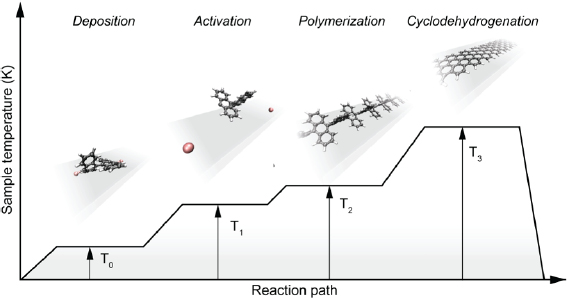
Figure I.2. GNR bottom-up synthesis concept. GNR synthesis is achieved by deposition of halogen-substituted precursor monomers at a substrate temperature T0, followed by their activation (halogen cleavage) at T1, polymerization at T2, and cyclodehydrogenation at T3.
Download figure:
Standard image High-resolution imageAll steps are accomplished at a pressure below 2 · 10−9 mbar while heating the sample to a specific T. In the first step, precursor monomers are deposited on a clean substrate held at T0. Quartz crucibles that are resistively heated up to the T needed are used for maintaining a precursor monomer flux of 0.1 nm per minute at the sample position, as determined with a quartz microbalance. The sample temperature is then raised to T1 for the halogen cleavage (activation) and to T2 for the polymerization of the activated precursors. Finally, GNRs are formed by triggering cyclodehydrogenation of the polymers by heating the growth substrate to T3 [37]. While each of these steps is crucial for GNR synthesis, not all of the intermediate products are easily accessible for structural characterization. E.g. monomer activation at T1 ideally leads to doubly activated precursor monomers (biradicals) that coexist with the cleaved halogens at the surface. Practically, however, this phase is often not accessible because the activated species frequently undergo polymerization directly at these T [21].
This implies that the activation barrier related to diffusion and covalent bond formation between the biradical species is smaller or equal to the energy barrier for halogen bond cleavage [38]. Deposition, activation, and polymerization steps can be combined into a single step by depositing precursor monomers directly at the polymerization temperature T2 = 450 K. The time for this combined step is the deposition time (1–10 min, depending on target GNR coverage) plus 15 min holding time [37]. This step is followed by the cyclodehydrogenation step, which is triggered by increasing the temperature to T3 = 630 K and holding it for 15 min. It is crucial not to exceed this T in order to avoid further activation of the formed GNRs. For higher T3 ≈ 660 K covalent crosslinking of GNRs was found [39], as well as the formation of GNRs of multiple widths related to partial edge dehydrogenation of GNRs, which triggers GNR fusion (cross-dehydrogenative coupling) to form seamless higher-order GNRs [39]. After cyclodehydrogenation, the sample is cooled to RT and either transferred to a connected scanning tunneling microscope for in situ characterization (see section IX.1) or directly taken out of the UHV chamber for characterization and/or further processing under ambient conditions.
The above mentioned parameters are valid for the growth of GNRs on Au(1 1 1), for which the highest quality is achieved for all reported GNR types [1726]. GNR synthesis under less stringent conditions was also reported [40]. Using a CVD setup, the synthesis of Chevron GNRs [41] and 9-AGNRs [42] were achieved.
An overview on published GNR structures is given in figure I.3. The most frequently used halogen atom is Br. The two main reasons for using Br is its better synthetic accessibility for most of the precursor monomers (as compared to I) and lower reactivity with the growth substrates (as compared to Cl [43]).
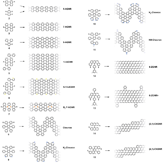
Figure I.3. Overview of bottom-up synthesized GNRs. X marks the leaving group, which is typically a halogen atom (X = Br, I, Cl). References are: 5-AGNR [44–47], 7-AGNR: [21], 9-AGNR: [48], 13-AGNR: [49], S-13-AGNR: [50], B2-7-AGNR: [51, 52], Chevron: [21], N2-Chevron: [53, 54], N4-Chevron: [55], NH-Chevron: [56], 6-ZGNR: [57], 6-ZGNR + : [57], (3,1)-ChGNR: [58], (4,1)-ChGNR.
Download figure:
Standard image High-resolution imageDepending on the choice of the precursor monomer, the selective synthesis of AGNRs with different width and bandgap was achieved [21, 44, 48, 49]. On-surface synthesis of ZGNRs was demonstrated for 6-ZGNRs using a methyl-based monomer design [57]. Chiral GNRs with a controlled sequence of armchair and zigzag segments along the GNR edge were made based on halogen-substitution of bianthryl [58]. GNRs with a controlled width-modulation along the axis, the so-called Chevron GNRs, were synthesized based on dibromo-substituted 1,2,3,4-tetraphenyltriphenylene [21]. This monomer design in particular, is well accessible for substitutional doping [54, 55, 1727]. Since chemical doping is achieved at the level of monomer synthesis, a fully controlled level of doping and periodic arrangement of the doping sites is reached in the final GNR. Chevron GNRs were fabricated with a number of nitrogen-substitution patterns [54–56]. For 7-AGNRs, substitutional boron-doping was achieved allowing to controllably modify the electronic properties [51, 52]. The combination of different precursors during the polymerization step gives access to different GNR heterostructures with additional opportunities, making specific electronic properties at the interfaces of dissimilar GNR segments available [48, 59–62]. Width-modulated GNRs were prepared, allowing to achieve distinct topological quantum phases [63, 64].
I.1.8. GNR characterization
The main method applied for developing new bottom-up synthesized GNR structures is in situ scanning tunneling microscopy (STM, see section IX.1). It allows accessing the growth at the surface-related synthesis steps by interrupting the growth protocol (figure I.2) after a specific step and, subsequently, transferring the substrate to a connected STM chamber. Beside coverage determination, STM was used for the determination of polymer length after the polymerization step as well as for the determination of possible undesired coupling motifs that can occur by either not entirely purified precursor monomer batches or a not fully selective monomer design, which potentially allows for covalent coupling configurations that are not compatible with the envisaged final GNR structure. With the exception of 5-AGNRs, polymerization of the activated precursor monomers yields structures where not all molecular subunits are planar with respect to the substrate surface [21, 48]. The related apparent height imaged by STM is for all monomers above 0.25 nm, higher than the apparent height of the final GNR structure (~0.19 nm). Using this sensitivity, STM allows for a direct access to the onset T of the cyclodehydrogenation step by identifying polymer segments, where lowered apparent height indicates the related planarization of the polymer to the final GNR. For the investigation of individual GNRs, T below ~25 K are needed to suppress their mobility on the surface (figure I.4).

Figure I.4. Characterization of 7-AGNRs on their growth substrate and after substrate transfer. (a) Large-scale STM topography image (bias: −0.5 V; current: 5 pA; T: 4.5 K; scale bar: 30 nm) showing high coverage 7-AGNRs on Au(1 1 1). Inset: small-scale STM image (bias: 0.1 V; current: 30 pA; scale bar: 3 nm). The apparent height of individual 7-AGNRs is 0.19 nm. (b) Constant-height nc-AFM frequency shift image (bias: 2 mV; oscillation amplitude: 0.3 Å; T: 4.5 K; scale bar: 1 nm) taken with a CO-functionalized tip. (c) Raman spectra of 7-AGNR on Au(1 1 1) recorded under ambient conditions after synthesis (green curve) with indicated peak positions of the main modes, and after transfer to Si/SiO2 (black curve; laser 532 nm, power of 2 mW, three scans of 20 s). (d) RBLM peak position for 5-AGNRs, 7-AGNRs and 9-AGNRs (red markers), together with predicted width-dependent RBLM wavenumbers for AGNRs [65].
Download figure:
Standard image High-resolution imageAn even higher resolution is achieved by using non-contact atomic force microscopy (nc-AFM) where the tip apex can be decorated with specific molecules or atoms to yield unprecedented insight into the chemical structure of the synthesized carbon nanostructures [66]. Tungsten tips attached to a tuning fork sensor [67] have been used in a low-T STM (ScientaOmicron) functionalized with CO molecules by dosing CO onto the surface and a controlled pick-up procedure [68]. By recording the frequency shift image at constant height (figure I.4(b)), the chemical structure of GNRs can be visualized with a resolution that is going down to individual chemical bonds. The sensitivity is high enough to resolve, e.g. additionally attached hydrogens at ZGNR edges (H2- instead of H-termination) [57]. With this unique structural sensitivity, nc-AFM is complementary to STM (see section IX.1), which is only indirectly sensitive to the atomic composition by recording an apparent structure defined by the local density of states near the Fermi level. The constant-height imaging mode, however, can only be applied to the flat final GNR structures [48]. Non-planar structures, such as the used precursor monomers and the polymer intermediates, are hardly accessible by nc-AFM due to the related 'constant height' imaging mode [66].
The main ex situ characterization tool applied to GNRs is Raman spectroscopy (see section IX.2/Raman) [1714]. Owing to their atomically defined structure, GNRs present well defined Raman peaks (figure I.4(c)). The main peaks are the G and D modes with overtones and the width-dependent radial-breathing-like mode (RBLM) (~396 cm−1 for 7-AGNRs) [40]. The D peak is intrinsic for GNRs due to the presence of edges [1715]. For laser energies ranging from 457 to 633 nm, between 1–2 mW power were used (higher power can result in thermal effects at ambient conditions [1725]). For laser energies in the infrared range (785 nm) a max of 10 mW is used [1725]. It is important to select the photon energy of the laser source close to the GNR bandgap to be in resonance [48]. For 7-AGNRs with an optical band gap of 1.9 eV [69], Raman spectra were recorded using a green laser (532 nm, 2.33 eV). For 9-AGNRs with an optical band gap of 1.1 eV [70], Raman spectra were recorded with an infrared laser line (785 nm, 1.55 eV). Exchanging the two laser lines for both examples leads to a loss of resonance conditions and the width-characteristic RBLM mode cannot be resolved anymore [1725].
I.1.9. GNR transfer
The on-surface synthesis of GNRs relies on the catalytic action of the metallic growth substrate, and therefore requires their transfer onto dielectric substrates for further characterization of their electronic or optical properties. Similarly, in order to explore GNRs as active materials in electronic or optoelectronic devices, their transfer to dielectric substrates is required. The potential of GNR-based devices was demonstrated by the realization of GNR-based field effect transistors (FETs) with an on current of 1 µA and on/off ratio of 105 [71, 72]. Furthermore, devices using CVD-GNRs as active material were reported with high on/off ratio and high photoresponsivity of 5 × 10⁵ A W−1 [41, 42]. Transfer was achieved using a sacrificial PMMA layer deposited onto the as-grown GNRs [72], stripped off after GNR transfer to the target substrate. A transfer method was developed allowing for the transfer of GNRs without PMMA, which avoids possible contamination problems related to PMMA residues [40, 55]. This relies on is delamination of Mica from a Mica/Au/GNR stack in an hydrochloric acid, from which the remaining Au/GNR stack is picked up with the target substrate. In a last step, the Au layer is then dissolved leaving a clean GNR film (without Au or iodine residues) on the target substrate. To do so, the Mica/GNR/Au stack was placed on concentrated (38%) hydrochloric acid (HCl) with the Au/GNR film facing up. After 15–20 min the mica detaches from Au. Once the mica is detached, the acid is removed from the container. In order to prevent sticking of the Au film at the container walls, it is important to not remove the acid completely in one step. After initially removing ¾ of the acid, water is added and the liquid removed in five iterative steps. In the last dilution step, the container is kept full of water for the pickup of the Au film with the target substrate. It is important that the target substrate is free of any impurities.
With the help of tweezers, the target substrate is approached (facing down) and pressed against the floating Au/GNR film until they stick together. The merged Au/GNR/substrate stack is then pulled out of the water. At this stage, the Au film is usually not completely flat on the substrate. In order to increase the contact between Au film and substrate, 1–2 drops of pure ethanol are added and dried under ambient conditions. Once dried, the Au/GNR/substrate stack is further heated on a hot plate (100 °C, 10 min). This two-step process results in a flattening of the Au film on top of the target substrate. The Au film was then removed by adding 1–2 drops of Au etchant (KI/I2, no dilution) on top of the Au film and waiting until the Au film was completely etched away (around 5 min). Finally, to clean the GNRs/substrate, this was soaked in water (5–10 min), rinsed with 20–30 ml of acetone/ethanol and water and finally dried under N2 flux [1725].
Using this method, 5-AGNRs, 7-AGNRs, 9-AGNRs and Chevron GNRs were transferred to SiO2, CaF2, Al2O3, glass slides and TEM grids (lacey carbon supported graphene, TedPella.com). The main characterization tool used to prove that the structure of the GNRs remains intact upon transfer was Raman spectroscopy. An example of Raman spectra taken before and after transfer of 7-AGNRs is in figure I.4(c)). All the characteristic 7-AGNR modes are present in the spectrum taken after transfer. Most importantly, the RBLM at 397 cm−1 remains equally intense and does not show significant broadening.
I.2. Graphene and carbon nanomembranes
CNMs with tunable properties can be produced by conversion of aromatic self-assembled monolayers (SAMs), CNMs can be then subsequently converted into GRM and graphene [73–80]. The process is schematically shown in figure I.5(a). First, a SAM is formed on a solid substrate, then the monolayer is converted into a CNM [81] via electron irradiation [82], and finally the CNM is transformed into GRM via annealing in vacuum (pyrolysis) or in an inert atmosphere. By tuning the structure of molecular precursors (figure I.5(b)), parameters of the self-assembly, substrate materials, electron irradiation and annealing conditions, GRM with adjustable crystallinity, thickness, porosity and electronic properties can be produced.

Figure I.5. Formation of CNMs and GRM from aromatic self-assembled monolayers. (a) Schematic illustration of the fabrication route for CNMs and graphene: Self-assembled monolayers are (i) prepared on a substrate then (ii) crosslinked by electron irradiation to form CNMs of monomolecular thickness. The CNMs are (iii) released from the underlying substrate, and further annealing at 900 °C transforms them into graphene. (b) Chemical structures of the different precursor molecules used for synthesis of CNMs and graphene. Figure adapted from Ref. [73], copyright American Chemical Society.
Download figure:
Standard image High-resolution imageI.2.1. Molecular self-assembly
Molecular self-assembly of aromatic molecules can be performed from solvents [73, 83] or by vapor phase deposition [84, 85]. For the self-assembly on coinage metal substrates such as Cu, Ag or Au, typically thiol functional groups are employed providing a covalent binding of the molecules to the substrate [86]. The solvent-based self-assembly of 1,1'-biphenyl-4-thiol (BPT, (1a), in figure I.5(b)), an aromatic precursor used for the production of SLG [74, 79] on Au substrates, can be conducted by immersing the substrate into a solution of BPT in dimethylformamide (DMF) [85]. Alternatively, a BPT SAM can be prepared by vapor deposition, i.e. exposure of sputter-clean Au substrates to BPT vapor [85]. Both methods allow the formation of BPT SAMs with comparable structural quality, although the solvent-based preparation typically results in a slightly higher (~5%) packing density of the formed SAMs. In case of the self-assembly from solvents the solvent/molecule interactions play an important role [86], and the packing density of the formed SAMs can be tuned by adjusting the solvent polarity and concentration of the precursor molecules [73]. In comparison to solvent-based self-assembly, self-assembly by vapor deposition requires high vacuum equipment, but SAM formation is achieved in a significantly shorter time (~1 h compared to 3 days [74, 84, 85]. For practical reasons, these different aspects have to be considered when designing the experiment. Furthermore, vacuum vapor deposition is preferred over solution deposition in the case of the formation of thiol-based SAMs on oxidative metal substrates (e.g. Cu or Ni), as the metal oxidation which hinders the self-assembly is avoided [84, 86].
I.2.2. Electron irradiation induced crosslinking of aromatic SAMs and formation of CNMs
Electron irradiation of aromatic SAMs results in lateral crosslinking of the constituting molecules and formation of CNMs [73, 82, 87]. The mechanisms of this process are discussed in Refs. [82] and [88]. Here, we summarize essential features of this process [89–91]. In aliphatic SAMs, electron irradiation results in significant (up to 80%–90%) molecular decomposition and desorption [92, 93]. In contrast, in aromatic SAMs the same treatment a thin carbon layer is formed. To induce the crosslinking in aromatic SAMs with low-energy electrons (50–100 eV), typically doses of ~50 mC cm−2, corresponding to ~750 electrons per molecule, are used. Because of electron irradiation, C–H cleavage takes place [90], which is the predominant process leading to crosslinking between adjacent aromatic rings. As suggested by UV photoelectron spectroscopy, quantum chemical and molecular dynamics calculations of BPT SAMs on gold, the formation of single- and double-links (C–C bonds) between phenyl rings of the molecules is expected during crosslinking [82]. This is supported by UV–vis spectroscopy of the formed CNMs [76]. Molecular dynamic calculations suggest [91] that a partial dissociation of the aromatic rings can take place and play a role in the formation of a carbon network. Such a mechanism would be in agreement with partial desorption of carbon in purely aromatic SAMs as observed by XPS. The XPS data also show that the irradiation and the subsequent molecular reorganization also affects the S-Au bonds. These structural changes at the molecule/substrate interface are in agreement with the LEED and STM results showing a loss of the long range (>5 nm) order in the SAMs upon electron irradiation [74].
Complete crosslinking of aromatic SAMs can be also achieved via He+ ion irradiation [94] with exposure dose ~1 mC cm−2, ~60 times smaller than the corresponding electron irradiation dose [82]. Most likely, this effect is due to the energy distribution of secondary electrons that have a maximum at energies below 50 eV, which results in a more efficient dissociative electron attachment (DEA) process. Crosslinking can also be achieved employing UV/EUV [83] and higher energy electrons (few keV) [95].
After electron irradiation of the aromatic SAMs, the CNMs can be separated from the original substrates and transferred using PMMA assisted transfer onto new solid or perforated substrates (e.g. grids, see section VI) [78], where they form large free-standing areas (up to 0.3 mm2). Figure I.6 shows helium ion microscope (HIM) images of free-standing CNMs from different types of aromatic molecular precursors [73]. These images show unbroken membranes, which demonstrate mechanically stable CNMs. CNMs with large free-standing areas up to ~0.3 mm2 can be obtained in this way. Since the thickness of CNMs is determined by the size of the precursor molecules and their packing in the SAMs, it can be tailored by varying these parameters enabling nanomembrane engineering. Figures I.6(a)–(c) show examples of CNMs where the thinnest nanomembrane has a thickness ~0.6 nm, while the thickest CNM is ~2.2 nm. Different CNMs have been fabricated and were investigated by HIM [73]. A relation between size and shape of precursor molecules, degree of order in its SAMs and the appearance of the CNM has been established [73]. If the molecule form a densely packed SAM (1(a)–(c), 2(a)–(c) and (e) in figure I.6(b)), the corresponding CNM is homogeneous and free of holes above 1.5 nm diameter. Figure I.6(d) shows a HIM image of such a CNM made from terphenylthiol (1c). Conversely, CNMs made from large molecules, i.e. hexabenzocoronenes (HBC, 3(b) and (c) in figure I.6(b)) or S,S'-(3',4',5',6'-tetraphenyl-[1,1':2',1''-terphenyl]-4,4''-diyl) diethanethioate (HPB, 3a in figure I.6(b)), form less ordered SAMs and exhibit pores, as presented in figures I.6(e) and (f). Here the dark spots are pores with diameters of 2–10 nm. Note that these pores have a narrow size distribution (see histogram insets). In case of the HBC precursor, the mean size of the nanopores is ~6 nm with surface density ~9.1 × 10¹⁴ pores m−2 The more compact HPB precursor shows a size ~2.4 nm with a surface density `1.3 × 10¹⁵ pores m−2. The formation of nanopores in these CNMs can be attributed to the large lateral dimensions of HBC and HPB molecules in comparison to smaller molecular precursors (see figure I.6(b)) and, in the case of HBCs, to the tendency of the disk like molecules to intermolecular stacking, which reduces the ordering in the respective SAMs. The average pore diameter correlates with the SAM thickness and decreases from 6.4 to 3.0 nm when the thickness increases from 1 to 2 nm [73].
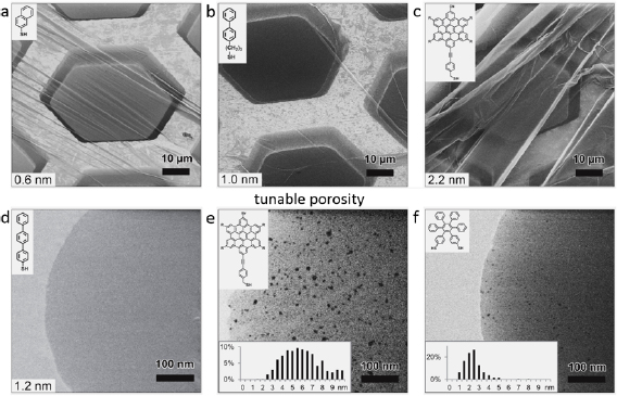
Figure I.6. Helium ion microscope (HIM) images of free-standing CNMs. After crosslinking the nanomembranes aretransferred onto TEM grids and images were taken at different magnifications (see scale bar). CNMs are prepared from: (a) Naphtalene-2-thiol (NPTH, (2a)); (b) 3-(biphenyl-4-yl)propane-1-thiol (BP3, (2b)). (c) 2-Cyano-11-(1'-[4'-(S-Acetylthiomethyl)phenyl]acetyl)-5,8,14,17-tetra(3',7'-dimethyloctyl)-hexa-peri-hexabenzocoronene (HBC-CN, (3c)); (d) [1'',4',1',1]-Terphenyl-4-thiol (TPT, (1c)); (e) 2-Bromo-11-(1'-[4'-(S-Acetylthiomethyl)phenyl]acetyl)-5,8,14,17-tetra(3',7'-dimethyloctyl)-hexa-peri-hexabenzocoronene (HBC-Br, (3b)); (f) S,S'-(3',4',5',6'-Tetraphenyl-[1,1':2',1''-terphenyl]-4,4''-diyl) diethanethioate (HPB, (3a)). The upper left insets show the precursor molecules. The CNMs in (a)–(c) are suspended over Cu grids, CNMs in (d)–(f) over Cu grids with thin holey carbon film. The numbers in the lower left corners in (a)–(d) indicate the CNM thicknesses, as determined from XPS before the transfer. HIM images e and f show CNMs with nanopores, the lower insets show the respective distributions (in%) of pore diameters (in nm). Figure adapted from [73], copyright American Chemical Society.
Download figure:
Standard image High-resolution imageI.2.3. Conversion of CNMs into graphene and GRMs via pyrolysis
I.2.3.1. Formation of nanocrystalline graphene/GRMs
CNMs are stable up to to 800 K [83], which enables their conversion into graphene/GRMs via pyrolysis in vacuum or inert atmosphere [73, 78]. The crystallinity of the produced GRM can be tuned by the annealing conditions, i.e. T and substrate material. The formation of nanocrystalline sheets by annealing of free-standing CNMs [78] on TEM grids (figure I.7(a)) was reported on Au, on [79] or SiO2[76, 77]. Although S is initially present in the CNMs both, XPS (of supported sheets) and scanning Auger microscopy (of suspended sheets), indicate that after annealing above 800 K all sheets consist only of carbon [78, 82]. At this T, the structural transformation of CNMs sets in, evident from appearance of the characteristic D-, G- and 2D peaks in the Raman spectra [96] [77–79]. This can also be visualized by HRTEM [73, 79]. As shown in figure I.7(b), after annealing of a BPT CNM (chemical formula (1a) in figure I.5(b)), most of the sheet area (~70%) is SLG recognized by the hexagonal arrangement of carbon atoms. Randomly oriented nanocrystalline graphene domains are connected with each other via heptagon-pentagon grain boundaries [97] (see inset to figure I.7(b)); a small fraction (~20%) of the sheet consists of bilayer graphene (BLG) as indicated by the Moiré pattern [98] and some of the area (~10%) shows an amorphous carbon phase [99].
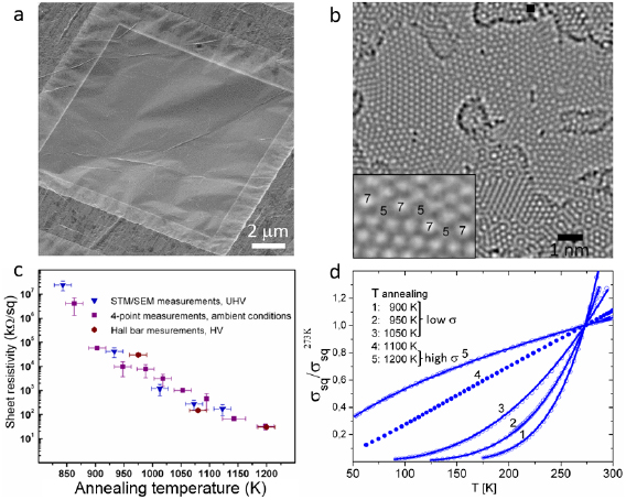
Figure I.7. Conversion of 1,1'-biphenyl-4-thiols (BPT) CNMs into nanocrystalline GRM upon annealing. (a) HIM image of BPT CNM annealed to 1000 K on a AuTEM grid. (b) Atomic structure of a similar sample obtained by aberration-corrected high-resolution TEM (AC-HRTEM, 80 kV). The inset shows a magnified grain boundary where arrangements of carbon atoms into pentagons and heptagons are highlighted. (c) RT sheet resistivity of the samples as a function of annealing T. (d) T dependencies of the normalized sheet conductivity demonstrate the change in electrical transport mechanism, i.e. insulator to metal transition. Figure (b) adapted from [73], figures (c) and (d) adapted from [79], copyright American Chemical Society.
Download figure:
Standard image High-resolution imageThe conversion of CNMs influences the electrical and optical properties [76, 78, 79]. Figure I.7(c) shows the sheet resistivity of BPT CNMs as a function of annealing T. The measurements were conducted at RT by different methods after respective annealing steps on both supported and suspended GRM [78, 79]. The non-annealed CNMs do not show lateral conductivity. Electrical conductivity is first detected after annealing at ~800 K. After annealing a ~1200 K the conductivity increases by six orders of magnitude approaching ~10 kOhm sq−1. To characterize the influence of this transformation on electrical transport, the T dependencies of the electrical conductivity, σ(T), and the electric field effect were studied in Hall-bar devices [79]. Samples with lower annealing T (900, 950 and 1050 K), (1–3) in figure I.7(d), have insulating behavior with a positive curvature in T. Their T dependence can be described by ![$ \newcommand{\e}{{\rm e}} \sigma \left( T \right)\propto \exp \left[ -{{\left( \frac{{{T}_{0}}}{T} \right)}^{\frac{1}{3}}} \right]$](https://content.cld.iop.org/journals/2053-1583/7/2/022001/revision1/tdmab1e0aieqn001.gif) , representing the Mott law [79], characteristic of thermally activated variable range hopping in a 2d system with weak Coulomb interactions [79]. For the sample with the highest degree of transformation, (5) in figure I.7(d), σ(T) shows a negative curvature with σ(T)
, representing the Mott law [79], characteristic of thermally activated variable range hopping in a 2d system with weak Coulomb interactions [79]. For the sample with the highest degree of transformation, (5) in figure I.7(d), σ(T) shows a negative curvature with σ(T)  T1/2, i.e. a semi-metallic state. Since the conductivity of nanocrystalline carbon in the insulating regime strongly depends on the density of states, a large ambipolar electric field effect is observed. The electron mobility in the resulting nanocrystalline carbon film~50 cm2 V−1 s−1 at RT [79]. The evolution of the transport characteristics upon conversion of CNMs into nanocrystalline carbon is reminiscent of that observed upon the thermal reduction of graphene oxide (GO) into reduced graphene oxide (RGO) [100, 101]. In both cases the final material presents an interconnected network of graphen nanocrystallites. However, in case of the RGO, a residual amount of oxygen containing groups is present [102], whereas nanocrystalline GRM sheets obtained by the conversion BPT CNMs consist only of carbon [73, 78, 79].
The thickness of the formed nanocrystalline sheets depends on the structure of precursor molecules, their ability to form SAMs and to be crosslinked into CNMs. Thus, by varying precursors (see figure I.5(b)), the thickness of the formed nanocrystalline sheets can be tuned by a factor ~3 [73]. The resistivity correlates with the thickness of the sheets, with lower resistivity for thicker sheets [73, 76]. An interesting opportunity is opened by using N- or boron-containing precursors, as in this case, GRM sheets doped by these elements can be expected, which are of interest for applications in catalysis [103] or energy storage [104].
I.2.3.2. Formation of polycrystalline graphene
Employing the conversion of CNMs into GRM by performing pyrolysis on catalytically active substrates like copper, graphene layers with high crystallinity and, therefore, high mobility above 2000 cm2 V−1 s−1 can be attained [74]. As a model system, the conversion of BPT SAMs is presented (see chemical formula (1a) in figure I.5(b)) into graphene on copper foils. The Raman spectroscopy data (see figure I.8(a)) show an evolution of the characteristic D, G and 2D Raman peaks as a function of T (see section IX.2/Raman for an introduction to the technique). The conversion of a CNM into graphene with T is clearly observed. For the highest annealing T (830 °C), the same features as known for single-layer graphene prepared by mechanical exfoliation (G peak at 1587 cm−1 and a narrow Lorentzian 2D peak at 2680 cm−1 (FWHM = 24 cm−1) [105] are observed after the conversion. The grown sheets were transferred onto grids and onto oxidized highly doped Si-wafers and were characterized by HRTEM and by electric transport [74]. The HRTEM and selected area diffraction (SEAD) data confirm formation of SLG [106], figures I.8(b) and (c). The dark-field TEM imaging shows that the formed sheets consist of graphene single crystals with lateral dimensions up to 1–2 µm [74].
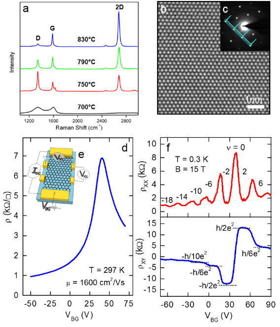
Figure I.8. Conversion of BPT CNMs into graphene on Cu foils. (a) Raman spectra (λexc = 532 nm) of the conversion of BPT CNMs as a function of T. The sheets after annealing were transferred from Cu onto Si wafers with 300 nm SiO2. (b) HRTEM micrograph of the sheet resolves the honeycomb lattice of graphene. The single layer nature can be determined from the HRTEM image contrast. It is further verified by the SAEDin (c). (d) RT resistivity in vacuum as a function of back-gate voltage using Hall bar devices schematically depicted in (e). (f) Quantum Hall effect at 0.3 K and 15 T. The upper plot shows Shubnikov–de Haas oscillations with the corresponding filling factors and the lower plot shows the Hall resistance as a function of back gate voltage, i.e. varied charge carrier density. Figure adapted from [74], © Wiley-VCH Verlag GmbH & Co. KGaA.
Download figure:
Standard image High-resolution imageElectric transport properties of the synthesized graphene films were studied by four-point measurements in the Hall bar geometry (see inset in figures I.8(d) and (e)) [74]. Figure I.8(d) presents the observed ambipolar nature as measured in a FET device. The RT charge carrier mobility, µ, extracted from the data at a hole-concentration of 1 × 1012 cm−2, is ~1600 cm2 V−1 s−1. µ values at lower charge carrier concentrations are ~2300 cm2 V−1 s−1. Further characterization of the transport properties (see section IX.3) at low T (T = 0.3 K) in a magnetic field of 15 T demonstrates that by varying the charge density with the back-gate voltage, Shubnikov–de Haas oscillations and resistivity plateaus of the quantum Hall effect specific for SLG are observed [107]. These results confirm the electronic quality of the grown sheets, l making them attractive for electronic applications.
I.2.3.3. Direct growth of graphenemicropatterns
Since only the electron-beam irradiated areas of SAMs undergo conversion into graphen, both large-area up to 10 cm2 and more graphene sheets and carbon films of various architectures (e.g. nano-ribbon, dot, anti-dot patterns) can be fabricated from SAMs by employing either defocused electron flood exposures [74, 78] or exposures by focused electron beams [75]. Because only electron-irradiated (crosslinked) regions of aromatic SAMs are converted into grapheneupon annealing, whereas non-irradiated (pristine) SAMs desorb from the surface [83], the suggested approach provides an opportunity to directly grow graphene patterns by area-selective electron irradiation [80], figure I.9(a). Therewith, at least four technological steps (spin-coating of photoresist, developing of photoresist, reactive ion etching, stripping of photoresist) employed in the conventional microfabrication of graphene electronic devices are omitted. Figure I.9(b) shows a graphene pattern grown on Cu at 800 °C after a BPT SAM is locally crosslinked by a primary electron beam of 3 keV and doses ranging from 75 mC cm−2 to 125 mC cm−2. The transfer of this structure onto a 300 nm SiO2/Si substrate is presented in figure I.9(c). By comparing the distances between the single structure elements in figure I.9(b) (on Cu) and 9(c) (on SiO2/Si), the structural integrity is conserved during transfer. Only a few elements show folding defects or missing parts. In this case, the local adhesion to the substrate is too weak to withstand the forces occurring during the removal of the transfer medium in solvent [80]. More advanced transfer techniques, like electrochemical delamination [108] or a clean-lifting transfer [109] may be applied to avoid or minimize the creation of defects (see section VI). The minimum size of the features in the grown pattern correspond to ~1 µm. The lateral resolution is defined in principle by the resolution of electron-beam lithography, ~7 nm for SAMs [110]. Another interesting opportunity is given by the fact that molecular self-assembly can be conducted on non-planar surfaces, thus it is also feasible to apply the developed methodology to create graphene structures on any 3d shape.

Figure I.9. Direct growth of patterned graphene. (a) Schematic of direct growth of patterned graphene. (b) SEM image of graphene microstructures directly written on top of Cu by irradiating a BPT SAM with a focused electron beam (3 keV, 75 mC cm−2 (left)—125 mC cm−2 (right)) and subsequent annealing (800 °C). (c) Same structure after transfer to a SiO2/Si wafer. Figure adapted from [80], © Wiley-VCH Verlag GmbH & Co. KGaA.
Download figure:
Standard image High-resolution imageI.3. Heterostructures from CNMs
Stacking of 2d sheets including SLG, hBN, or TMDsinto layered materials heterostructures (LMHs) have led to novel materials with a potential for applications and in fundamental research [111, 112]. The integration of other low dimensional materials into these LMHs can extend these borders even further. Here a modular and broadly applicable route is presented to create hybrid LMHs made of individual ~1 nm thick Janus CNMs (JCNM) [113] functionalized with other low-dimensional materials (see figure I.10).
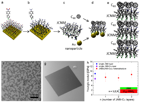
Figure I.10. Hybrid LMH of 0d and 2d carbons. (a)–(e) Schematic representation of the LMH assembly. (a) Formation of a NBPT SAM on Au. (b) Electron irradiation induced crosslinking and reduction of the terminal nitro groups into amino groups. (c) Formation of a free-standing JNM with the terminal N- and S-faces. (d) Functionalization of the N- and S-faces with C60 and AuNPs. (e) Assembly of a (C60–JNM)n (here n = 3) hybrid heterostructure by mechanical stacking. Color code for atoms: black—C, grey—H, blue—N, green—S, and red—O. (f) HIM images in the scanning transmission ion mode shows the immobilization of 16 nm Au NPs on a JNM which are uniformly distributed with an coverage ~50%. (g) HIM image of an JNM-(C60–JNM)3 heterostructure spanning a Si window. (h) Young's moduli of JNM, C60–JNM and JNM-(C60–JNM)n (n = 1, 2, and 3). Figure adapted from [113], with permission of The Royal Society of Chemistry.
Download figure:
Standard image High-resolution imageJCNMs are produced via electron irradiation induced crosslinking of 4'-nitro-1,1'-biphenyl-4-thiol SAMs and have different chemical groups on their opposite faces, e.g. amino groups on the top side (N-side) and sulfur species on the lower side (S-side) [114]. They can be independently chemically functionalized with desired building blocks and assembled into hybrid LMHs via stacking, figures I.10(a)–(e). C60was covalently bound to the amino groups on the N-side of a JCNM [113]. To demonstrate that in the assembly of hybrid heterostructures also the S-side of JCNMs can be used, it was functionalized with Au NPs, figure I.10(f). The possibility of bifacial chemical functionalization of JCNMs paves the way to hybrid LMHswith a variety of other 0d and 1d materials.
In Ref. [113], cm2-sized heterostructure stacks of hybrids JNCM with coupled C60 were fabricated. They were characterized with respect to their structural, chemical and mechanical properties. The characterization by XPS (see section IX.2) shows that the chemical composition and effective thickness of the individual C60/JCNM layers remains unaffected [113]. Individual C60/JCNMs and their heterostructures were further studied by mechanical bulge tests [133] to characterize their mechanical properties. To this end, the sheets were transferred onto a Si substrate with an array of square shaped orifices. Figure I.10(g) shows a HIM image of a homogeneous free-standing hybrid structure of three layers C60/JCNM spanning over an orifice with dimensions of 40 × 44 µm2. The LMH can support its own weight and preserves its mechanical integrity. The Young's moduli of C60/JCNM multilayers were measured by mechanical bulge tests and are presented in figure I.10(h). Within the accuracy of the measurement, the Young's moduli have similar values, demonstrating that the mechanical properties are not degraded upon the assembly of the hybrid.
II. Top-down
II.1. Precursors
A wide variety of GRMs with different characteristics can be obtained through liquid phase techniques [111, 115]. For a given approach, the selection of an appropriate precursor allows to tune the final features and properties of the GRM products in order to optimize their performance for each application. Graphite is the reference starting material to produce graphene, but it presents different characteristics like particle size, crystal size or purity, which have to be considered. E.g., graphite with small crystal size will limit the maximum lateral size of the final graphene flakes. Other precursors, such as nanocarbons (i.e. carbon materials with nanoscale size, such as CNTs) [17, 116, 117] or pre-graphitic carbons (short ranged ordered amorphous carbons) [118, 119] have been also investigated as potential candidates for graphene production, as discussed below.
II.1.1. Graphite
Graphite consists of stacked graphene layers bonded by van der Waals (vdW) forces [120]. Carbon atoms are hexagonally arranged and SLGs are parallel to each other. Graphite has two main allotropic forms, hexagonal [121] (figure II.1(a)) and rhombohedral [122] (figure II.1(b)). In both cases the carbon hybridization is sp2, the C–C distance in the basal plane is 0.1417 nm, and the distance between the layers is 0.3320 nm. The hexagonal form is the most stable, with layers stacked in an ABAB sequence (unit cell constants: a = 0.2456 nm, c = 0.6708 nm) [121]. In Rhombohedral graphite the sequence of the layers is ABCABC (unit cell constants: a = 0.2566 nm, c = 0.100 62 nm) [122].

Figure II.1. (a) Hexagonal and (b) rhombohedral structures of graphite.
Download figure:
Standard image High-resolution imageGraphite can be natural or synthetic. The latter can be obtained by subjecting nongraphitic carbons as pitches and cokes to high temperatures (1700 °C–2700 °C) in inert atmosphere or vacuum [123–125].This is the case of graphitizable carbons, i.e. non-graphitic carbons which, upon thermal treatment, convert into graphitic carbon, [126]. The degree of graphitization, the amount of disordered phase converted in their graphitic counterpart, can be further increased by performing thermal treatment under high pressure (100–1000 MPa) [127]. Graphitic materials can also be obtained by CVD of hydrocarbons, such as methane [128] or ethane [129] at T ~ 1200 °C or by catalytic (c-CVD) and these synthetic methods are reviewed in section V.
Graphene can be obtained by exfoliation of graphite [130]. The presence of defects in the layers leads to graphene with lower conductivity [120, 131–134]. Graphite with large crystal size allows one to obtain bigger flakes [132]. The crystal boundaries of the starting graphite have an impact on the amount and type of oxygen functional groups introduced in the oxidation reaction resulting in GO [132], influencing also the sonication time required to overcome the vdW interactions [133], as well as the chemical structure of the RGO obtained after thermal [135] or chemical reduction [135]. The microstructure of graphite can be distinguished by polarized light microscopy [120], where the different crystalline domains are defined by the interference colours (figure II.2(a). Figure II.2(b) shows anSEM image of graphite in which these features cannot be observed. The distribution of crystal size also influences the polydispersion in lateral size of the obtained GO/RGO material, limiting the maximum lateral size. The final average size of graphene is usually much smaller than the initial crystal size in graphite, and is mainly dictated by the mechanical process of exfoliation at the meso- and nano-scale [136, 137].
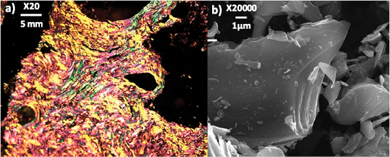
Figure II.2. (a) Optical micrograph acquired with an oil-immersion objective (20×) and an one-wave retarder to generate interference colours and (b) SEM picture of the same graphite.
Download figure:
Standard image High-resolution imageGO/RGO has been prepared from different natural graphites [138]: flaky, (natural graphite of finely powdered crystalline graphite with grain size smaller than 250 µm), lumpy (crystalline graphite with a walnut to a pea size), and amorphous (exhibiting only short range order) [139, 140]. Lower crystallinity of the parent material (lumpy > natural > amorphous) leads to higher defects, smaller GO sheets' size and higher surface areas (figure II.3). Natural graphites can contain silicates and other particles that can contaminate the final GRM, as detected by thermogravimetric (TGA) measurements [141].

Figure II.3. Schematic model of partially reduced GO and their parent graphites.
Download figure:
Standard image High-resolution imageSmaller particle size will result in higher content of oxygen functional groups in GO, because of easier diffusion of reagents during oxidation. This influences the final electrical and thermal properties [142, 143]. Graphite with particle sizes >200 µm are adequate for the production of GRM to be used in thermoset composites by infusion [144]. Particle size >600 µm are ideal for conductive thermoset composites [145].
The discrete particle size of graphite, as observed in SEM, is different than the particle size determined by other techniques such as laser diffraction, optical microscopy or granulometry. Laser diffraction or granulometry increase the measured particle size of graphite due to the agglomeration of discrete crystals. SEM can distinguish between different or discrete crystals and allows the measurement of particle size with more accuracy. In the case of optical microscopy, it is more difficult to separate particle sizes.
Expanded graphite is a graphite-derived material formed by a two-step oxidation-reduction process that retains the long-range-ordered layered structure of graphite, yielding a large interlayer distance. It can be used for the preparation of GRM by liquid methods [147]. Typical expanded graphites used for the preparation of graphene flakes have a medium diameter D50, i.e. the value of the particle diameter at 50% in the cumulative distribution of particle size diameters, from 15 to 50 µm.
II.1.2. Non-graphitic carbons
Non-graphitic carbons were also proposed [148, 149] as precursors for the synthesis of GRM by top-down techniques. e.g. petroleum and coal-tar pitches pass through a liquid or liquid-crystalline phase when subjected to heat treatment in inert atmosphere [150]. These materials are graphitizing and develop a graphitic microstructure upon heating to 3000 °C [151]. When these precursors are carbonized at lower temperatures (1000 °C), they become cokes. A coke is a solid carbonaceous material derived from distillation of low-ash, low-sulphur bituminous coal, or derived from oil refinery coke units or other cracking processes [152]. It has a partially organized lamellar structure resulting from the parallel stacking of layers of sp2-hybridized carbon atoms. Therefore, Refs. [148, 149] suggested that these could be used for the preparation of graphene flakes. Since high T (up to 2500 °C–3000 °C) are required to obtain synthetic graphites, the direct use of cokes as precursors reduces the environmental impact of the whole process. Moreover, the broad range of microstructures and chemical compositions of cokes (as determined by the carbon source and the carbonization conditions) makes them a suitable starting material for the synthesis of graphene or GO with targeted structures and compositions.
Due to the different microstructure and chemical composition of cokes and graphites, the conditions for the synthesis of GRM should also be adjusted. Thus, compared to graphites, cokes require larger amounts of reactants during their oxidation by the Hummers' method. Otherwise, its exfoliation into GO would have a much lower yield [148]. When cokes and graphites were exfoliated in NMP, flakes from coke had a larger number of defects and smaller lateral size (~400 nm) than those from graphite (~1 µm) [148]. Similarly, as the crystallinity of cokes increases, its subsequent exfoliation yields flakes with larger lateral size and in higher yield [149].
II.1.3. Nanocarbons
CNTs or nanofibres (CNFs), have also been explored as alternative precursors to produce graphene sheets and GNRs in liquid media [17, 116, 117]. Twisted ribbon-shaped carbon nanofibers are helical carbon nanofibers comprising 5–6 stacked graphene layers [117, 153–155]. Two approaches have been proposed for the production of graphene flakes and sheets from these [153, 154]. The first is based on a mechano-chemical method, through melamine intercalation during ball milling in different solvents such as isopropanol, THF or DMF. Ref. [153] produced graphene suspensions in low boiling point solvents such as 2-propanol (~83 °C) and THF (66 °C) by a scalable method [153]. Ref. [154] obtained GO/RGO flakes® using the Hummers' method [156] and different reduction techniques [154, 157, 158].
GNRs have been produced from CNTs as the starting material by solution-based oxidative processes [17, 117]. CNTs suspended in concentrated H2SO4 were oxidized by adding KMnO4 (500 wt%with respect to CNTs) at T < 70 °C [17].The resulting GNRs have straight edges and are dispersible in water and other polar solvents due to the presence of oxygen moieties. Unzipping single-wall carbon nanotubes (SWNTs) [17] gives GNRs, but these are difficult to disentangle. Multi-wall carbon nanotubes (MWNTs) led to less entangled GNRs [17], that can be separated to single layers after sonication. Carbonyls, carboxyls and hydroxyl groups present in the GNRs can be reduced by treatment with aqueous hydrazine (N2H4·H2O) after dispersing them in aqueous sodium dodecyl sulphate in order to prevent their re-aggregation. CNT unzipping by intercalation of lithium and ammonia and subsequent exfoliation was also reported [116]. However, this procedure yields a mixture of multilayer GNRs, partially open MWNTs, and flakes, contrary to oxidation with KMnO4, which allows a nearly 100% yield of GNRs with no presence of partially open MWNTs [117].
II.2. Liquid phase exfoliation
Various strategies have been developed to produce colloidally stable GRM dispersions. They can be classified into intercalation-based methods [159–161], and methods relying on mechanical exfoliation and further stabilisation by suitable solvents/surfactants (LPE) [161–164]. Oxidative intercalation of graphite and subsequent delamination to yield GO are amongst the oldest techniques [156].
LPE is one of the simplest and most versatile strategies to obtain colloidally stable dispersions from a broad range of LMs. Energy in the form of sonication or shear is used to overcome the van der Waals attraction in bulk LM. If this is done in a suitable liquid (solvents with matching solubility parameters, or additives that act as electrostatic and/or steric stabilizers [165]), reaggregation is prevented. The resulting flakes can have low defect densities, and can be further solution-processed by a range of techniques [166]. LPE of MoS2 and WSe2 was reported in 1989 [167].
While LPE is a versatile method for producing large quantities of flakes from bulk powders, it has some disadvantages. The flakes are highly polydisperse with a range of sizes and thicknesses (lateral sizes ranging from tens of nanometres to tens of microns, number of layers (N) from 1 to 100 s of layers). The dispersions can also have low monolayer content (YM < 1%). A precise, statistical analysis of size distribution due to exfoliation by ultrasound has been reported, for GO sheets [136]. For application areas where LPE flakes are well suited, such as printed optoelectronic and electrochemical devices, optimized performance is unlikely to arise through direct use of the pristine dispersions. This is especially true for those applications requiring direct bandgap luminescence of transition metal dichalcogenides (TMDs). Thus, size selection must be an integral part of the production process [168].
Many strategies exist for both exfoliation and size selection, depending on the starting material and the desired outcome. A number of review articles on exfoliation in liquid media have been published [115, 161–164, 166, 168–170, 172, 173]. Here, questions such as which medium (e.g. solvent or surfactant) or exfoliation method (e.g. sonication or shear) is more suitable and how to size-select flakes using benchtop centrifuges are addressed.
II.2.1. Choice of medium
II.2.1.1. Solvents and detergents
In a typical LPE experiment, the bulk crystal is immersed into a liquid and subjected to sonication [131, 162, 173–175], shear mixing [176, 177], microfluidization [178], ball milling [179] or similar [180, 181]. Prior to designing an experiment, thought needs to be given to the choice of medium. This can be crucial and will often depend on the starting material in combination with the exfoliation method and the purpose of production. Irrespective of the exfoliation method and/or medium, a purification step of the starting materials (e.g. graphite flakes) is useful, since these may contain impurities that can destabilize the dispersion.
Aqueous surfactant solutions are widely used as stabilizers in LPE [172, 182–184]. Usually, xfoliation, stabilization and size selection is quite robust and reproducible giving access to long-term (weeks-months) stable, dispersions. In order to retain 'pristine-like' optical properties, similar to those of micromechanically cleaved (MC) materials, aqueous surfactant solutions are of advantage. E.g., photoluminescence (PL) of MoS2 and WS2 can be observed in single layer (1L)-enriched solutions in sodium cholate (SC) with emission dominated by excitons and at similar spectral positions as MC TMDs [185, 186]. Surfactants such as SC are water soluble and do not require the same level of health precautions as organic solvents [187]. SC is compatible with many processing techniques such as vacuum filtration and spraying. However, printing from aqueous surfactant still remains challenging, as it is difficult to control the rheological properties [166]. In addition, there are two other downsides. First, some materials (such as GaS [188] or black phosphorus [189, 190]), can degrade in the presence of water/oxygen [189, 191] so that aqueous surfactant solutions cannot be used. Second, it is difficult to completely remove the surfactant from the resulting flake surfaces after processing, as it can be trapped between restacked flakes, potentially deteriorating the resulting network properties. A few systematic studies (see [161–164, 166, 168–173, 192]) exist on the impact of the chemical structure of the surfactant or its concentration on the degree of exfoliation, i.e. N or yield of 1L and few layer (FL) flakes as well as their lateral size, with detailed data available for SC or sodium dodecyl benzene sulfonate (SDBS). However, a comprehensive picture is still lacking due to the vast parameter space (materials, surfactants, concentrations, exfoliation techniques, centrifugation procedure). Systematic studies on the effect of less common surfactants, such as polycyclic aromatic hydrocarbons (PAH), have also been reported, correlating the adsorption energy of the single molecule on graphene to the overall exfoliation performance [193, 194]. Flakes produced in aqueous surfactants are smaller, but also thinner than in solvents such as N-methyl-2-pyrrolidone (NMP) and N-Cyclohexyl-2-pyrrolidone (CHP) [174]. This is most likely related to the higher viscosity of these solvents compared to aqueous surfactant. This can on the one hand hinder intercalation of the solvent between the layers of the crystals during the exfoliation process and in addition lead to a slower sedimentation in the centrifugal field [195] and hence a larger population of larger/thicker nanosheets. Details on differences in sizes/thicknesses and yields of 1L and FLstrongly depend on material, exfoliation conditions and centrifugation conditions making it difficult to quantify these effects.
Solvent stabilisation can be described in the framework of solubility parameters [196]. Solvents or solvent blends can stabilize liquid-exfoliated flakes and prevent them from reaggregating, when solubility parameters, such as surface tension or Hansen parameters, of solvent and solute match [131, 174, 197–200]. Chemically unstable materials, such as black phosphorus (BP), can be protected against degradation through a stabilising solvation shell [190]. In addition, it is easier to tune rheological properties for processing techniques such as inkjet printing [201] and solvent removal is typically easier than for surfactants. However, certain solvents, such as NMP or ODCB, can degrade and polymerize [202, 203], changing the properties of the exfoliated material, while hampering subsequent spectroscopic and microscopic characterization [204]. In such cases, the solvent can also remain on the flakes surfaces. In general, good solvents show a strong, yet noncovalent interaction with the flakes, altering optical properties as, e.g. manifested by PL shifts in TMDs [186]. Another consideration is that many suitable solvents, such as NMP, suffer from high boiling points (>200 °C) and are often toxic [205]. Some solvent blends have been identified as promising (e.g. alcohols and water) [206, 207] to potentially overcome the limitation of the high boiling point solvents.
GRM dispersions in water can also be stabilized by using a wide range of polymers [182, 208–212], such as ethyl cellulose (EC) [209], cellulose acetate (CA) [208], lignin [211], polyvinylpyrrolidone (PVP) [210], and even more complex systems [182, 212]. The use of polymers as stabilizing agents in the LPE process works better than the use of small organic molecules in terms of the concentration of graphene dispersions. Yet, because of the strong polymer/graphene non-covalent interactions, flakes produced by exploiting this approach cannot be completely separated from the polymer/graphene composites [213].
II.2.1.2. Molecule-assisted LPE
Stable dispersions of graphene in water have also been obtained using small polyaromatic dyes as surfactants [194, 214, 215]. Thanks to their aromatic core, these molecules can adsorb strongly on the graphene surface (EADS ~ 15 Kcal mol−1), forming also ordered layers [193]. They have also a strong (molar absorption coefficient ε > 15 000 l g−1 m−1) and unique absorption and emission spectra in the visible range, which allows to monitor their interaction with graphene in solution and in solid [216, 217]. Many of these molecules are low cost (<100 $ Kg−1) dyes, widely used in large-scale compounding of polymers, e.g. as industrial additives and colorants dyes [218]. While most of the work has been done with graphene- where a strong interaction of the aromatic core of the dye with the extended π-electron network of the flakes occurs, these molecules can also be used to exfoliate a wide range of LMs, such as BN [219], WS2 [219] and MoS2 [219], selenides and tellurides [219].
The use of properly selected small PAH organic molecules or polymers can enhance the exfoliation of graphite, in particular when the molecules/polymers possess a high (EADS ~ 15 Kcal mol−1) energy of adsorption on the basal plane of graphene. However, these molecules or polymers do not act as graphene dispersants or graphite exfoliators, i.e. they do not trigger the exfoliation. These molecules/polymers mainly act as dispersion stabilizing agent via the non-covalent functionalization, i.e. through the adsorption of their hydrophobic moieties on the graphene surface during the process of exfoliation [165]. Therefore, they can prevent re-aggregation and increase the stability of both aqueous and organic dispersions [165].
Using water as a LPE media is a natural choice because of its non-toxicity and offers potential for the formation of biocompatible graphene-based materials for biomedical applications [220]. Yet, LPE of graphene in water is particularly challenging due to the hydrophobic nature of the sheets. This challenge can be overcome by using surfactants such as SC, which allow exfoliated flakes to remain suspended. Among various molecular stabilizers, PAHs [221, 222], substituted with numerous side groups, are the most studied compounds. Adsorption of PAHs onto the graphene surface occurs through π–π interactions between the planar π-conjugated surfaces. In these noncovalent interactions, both PAHs and flakes surfaces share the π-orbital electrons, ultimately resulting in the reduction of the surface free energy of the dispersion [194]. Various derivatives have been used to stabilize CNTs dispersions [223], and as in the case of NMP, they have been adopted for LPE of graphite [194, 224–226]. Nevertheless, not all stabilizers suitable for CNTs, having a curved surface, would be ideal for dispersing graphene with a flat surface. Because of the improvement of the exfoliation yield (the amount of solubilized material during LPE) and, in particular, increase in the number of SL in LPE in the presence of small PAHs such as pyrenes, NDIs, [227] and PDIs [228], and other PAHs are also expected to be suitable to stabilize graphene produced by LPE.
Regardless of the exfoliation yields (% of SL, concentration) and the stability of graphene in aqueous dispersions, the use of water as an exfoliation medium is not recommended for electronic devices such as FETs. The presence of water at the interface with the dielectric substrate can enhance charge-trapping [229]. Therefore, the use of stabilizers in organic solvents has also been explored [230–235]. For more details on the underlying specific noncovalent interaction, see section VIII.3.
II.2.2. Exfoliation methods
II.2.2.1. General considerations
The purity with respect to contaminations of the commercially available materials is often unpredictable, creating problems for the reproducibility in the exfoliated product. Accordingly, the general recommendation is to perform a two-step exfoliation process [185, 186, 236]. In the first one, the material in the medium of choice is subjected to a short (~20% of the time of the total planned duration) exfoliation. After this initial step, the dispersion should be subjected to centrifugation at intermediate centrifugal acceleration (~5000 g) after which the supernatant is decanted and discarded and the sediment collected in fresh solvent/surfactant. This can then be followed by a second, longer exfoliation. This approach allows most of the impurities (and very small flakes) to be removed. This is particularly needed when working with ionic surfactants, as the impurities are often ionic and therefore, can destabilize the surfactant dispersion via charge screening effects.
A higher initial concentration of the precursor bulk material will also give a higher concentration of exfoliated flakes, up to when the dispersed concentration saturates. This initial concentration is typically >30 g l−1 of precursor concentration [174, 176, 177, 188, 190, 237–240]. Similarly, longer processing times yield higher dispersed concentrations [174, 176, 177, 188, 190, 238–242]. While this can also change the length and thickness distributions in the as-obtained dispersion [241], this effect can be balanced by appropriate size-selection techniques [168].
The choice of the exfoliation method is material dependent. E.g. while graphite is readily exfoliated for various methods [176, 177, 237] (sonication, shear, microfluidization, ball milling), this may not be the case for other materials. In particular for TMDs, the quality of exfoliation (as measured by the concentration/yield of 1L and 2–5 L flakes is better when using tip sonication compared shear mixing [176, 238]. For GaS, bath sonication is most effective [188]. When attempting to exfoliate a new material, it is important to not only consider the stabilizer, but also to test various available exfoliation methods. In particular the role of the crystallite size of the starting material in combination with the exfoliation method has not been investigated systematically.
II.2.2.2. Sonication
Sonication can be performed in tip or bath sonicators. In tip sonication, energy is imparted to the dispersion media directly [243], whereas in the sonic bath, the energy must travel through the tank and dispersion vial before reaching the flakes [243]. Although the scalability of sonication to produce few layer flakes has not been demonstrated (compared with shear exfoliation and ball milling), tip sonication remains useful as lab-scale technique, as the material quantity (hundreds of mg) is generally sufficient to test size-dependent properties in a range of application areas.
For LMs, tip sonication is preferred over bath sonication due to the higher production rates, (i.e. more exfoliated material is produced in shorter times, with concentrations in the range of ~1 g l−1 in <24 h for initial bulk material concentrations of 30–50 g l−1) [174, 186, 244]. In this case, various sonic tip configurations are available with different probe sizes and shapes and processors. In typical protocols [185, 186, 245, 246], solid flathead tips are used at sonication amplitudes ~60%–75%. At lower amplitudes, exfoliation can be poorer: the mean N WS2 increased by ~1 (across eight size-selected dispersions) for sonication at an amplitude of 50% compared to 60% [246]. From experience, higher amplitudes can damage the processor after prolonged (100 s of hours) use. 500 and 750 W do not give noticeable differences [246]. Since the sonic energy falls off exponentially from the probe [243], it is important to match the container to the probe size as recommended by manufacturers. Even though the dispersed concentration of FL flakes increases with sonication time [174, 176, 177, 188, 190, 238–242], 5–7 h of sonication provides a compromise between dispersed concentration and time.
It is crucial to prevent heating of the sample, especially in tip sonication, but also in bath sonication, shear exfoliation, etc. This is not only because heating can deteriorate the properties of the material, but also because dispersed concentrations are lower. While cooling in tip sonication can be achieved by positioning the reaction vessel, i.e. a metal cup in an ice bath, it is far more ideal to install a chiller, as the ice must be replenished every 2 h or so [245]. In addition, keeping the dispersion cool is facilitated by pulsing the sonication through the device controller. For a given combination of sonicator, operating conditions, cooling, sonication time and material, the outcome of tip sonication appears reproducible both in terms of dispersed concentration and size distribution [185].
In general, bath sonication may offer a lower-cost alternative to tip sonication, and additionally, in some cases, such as for GaS [188], this is preferred because tip sonication can damage the exfoliated flakes. The energy input is lower in bath sonication [243], as it is less. Therefore, less material fragmentation is expected. However, longer processing times are required (depending on material) to achieve an equivalent concentration of dispersed material compared to tip sonication. For TMDs, sonication times are longer by a factor ~20 in bath compared to tip sonication. In general, bath sonication is less reproducible than tip sonication, and the outcome varies depending on specific bath used, filling level of the bath, and positioning of the vial within the bath. While more reproducible results can be obtained by rotating the sample in the bath during sonication, this will result in a lower dispersed concentration for an equivalent sonication time compared to placing vials in 'hot spots' (thermolytic centers, where the sonication induced cavitation bubbles of the water in the tank preferentially collapse). Again, it is important to prevent heating of the sample (at least for non graphene LMs) by either installing a cooling system or exchanging the water every 30 min.
II.2.2.3. Shear exfoliation
Alternatively to sonication, one can use shear exfoliation in rotor stator mixers [176] or in blenders with rotating blades [177, 238]. Even a kitchen blender can be used, offering a very low cost alternative to sonication [177]. However, the household kitchen blenders are not designed to operate in organic solvents and can be destroyed when doing so. In addition, continuous operation heats up both sample and mixer, so that the run has to be paused frequently (after 15 min) and mixer and sample cooled in an ice bath. The dispersed concentration of FL flakes is not strongly dependent on the processed volume, so that shear exfoliation is a scalable process with production rates of 0.15 g h−1 for graphene and 1.3 mg min−1 for MoS2 [176, 177, 238]. The quality of the material in terms of dispersed concentration and mean N is comparable to sonication in the case of graphene [177].
II.2.2.4. Microfluidization
Microfluidization is a homogenization method that applies high pressure (up to 207 MPa) [247] to a fluid forcing it to pass through a microchannel, figure II.5. The key advantage over other LPE methods is that high shear rates ( > 106s−1 [248, 249]) can be applied to the whole fluid volume [249], not just locally. Microfluidization was used for the production of polymer nanosuspensions [247], in pharmaceutical applications to produce liposome nanoparticles with diameters smaller than 80 nm to be used in eye drops for drug delivery to the posterior segment tissues of the eye [250], or to produce aspirin nanoemulsions [251], as well as in food applications for oil-in-water nanoemulsions [252]. Microfluidization was also used for the de-agglomeration and dispersion of CNTs [253].
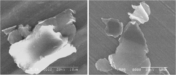
Figure II.4. SEM images graphite 0–200 µm (>0.2 mm; 10% max) and a graphite 0–600 µm. Adapted from [146].
Download figure:
Standard image High-resolution image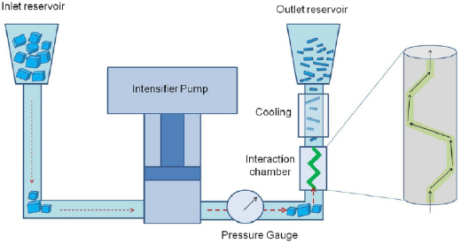
Figure II.5. Schematic of microfluidization process. Graphite flakes in SDC/water are added in the inlet reservoir. An intensifier pump applies high pressure (207 MPa) and forces the suspension to pass through the microchannel of the interaction chamber where intense  ~ 9.2 × 10⁷ s−1 is generated. The processed material is cooled down and collected from the outlet reservoir. The process can be cycled several times [178]. Adapted from [178].
Download figure:
Standard image High-resolution imageThe main step of this process involves placing the graphite/solvent mixture into an inlet reservoir. An intensification pump, driven by electro-hydraulics, provides two motions, suction and compression, drawing a portion of sample into the processor through a one-way valve, and then pushing this sample fraction past the pressure gauge and through sub-millimetre sized channels within a diamond interaction chamber, where graphite exfoliation takes place [178].
Interaction chambers are typically based on two geometries, Y- and Z type. The Z-type chamber is preferred for graphite exfoliation, since the geometry consists of sharp turns and a narrow rectangular cross-section for optimal shear. The chamber G10Z is ~87 µm in diameter. The motion of the intensification pump creates mixing within these micro channels, generating pressures > 30 000 psi (~2100 bar). The fluid dynamics of the process can be turbulent or laminar as defined by the Reynolds number, dependent on the kinematic viscosity and density of the solvent used [178].
Below are two typical recipes for the production of graphitic flakes without centrifugation (Method 1), or FLGs following centrifugation (Method 2). Due to the dimensions of the interaction chamber, microfluidic processing of large (>100 µm) graphite flakes may block the microfluidic channel. Instead, smaller powder sizes are advisable (typically, the particle diameter corresponding to 90% cumulative (from 0 to 100%) of the undersize particle size distribution (D90), less than 30 µm).
II.2.2.4.1. Method 1: production of multi-layered flakes
This method [178] refers to the production of high yield (100 wt.%), high concentration (up to 100 g l−1) graphene-based inks that are not centrifuged. Graphite powders (natural or synthetic, particle size <30 µm) are mixed at a concentration up to 100 g l−1 with SDC at a concentration 9 g l−1 in water in typical batch sizes of 250–500 ml. The material is collected in a beaker and placed back in to the inlet reservoir to cycle automatically for the desired length of time depending on the number of process cycles, n (where n is typically <70). The final product is collected. Sodium carboxymethylcellulose (NaCMC) (10 g l−1) is added whilst stirring to adjust the viscosity to the required value. NaCMC is slowly added until fully dissolved in order to avoid the formation of clumps. Clumps that are formed should be ground with a spatula and the ink left to stir overnight.
Figure II.6 shows SEM images of the coatings comprising the starting graphite (figure II.6(a)), after 5 (figure II.6(b)) and 100 cycles (figure II.6(c)). Flake size reduction and platelet-like morphology is observed after microfluidic processing.

Figure II.6. SEM images taken from coatings comprising (a) starting graphite, (b) after 5 cycles and (c) after 100 cycles. Reproduced from [178].
Download figure:
Standard image High-resolution imageSince these inks are not further processed by centrifugation, YW (yield by weight) is 100 wt.%. 4 wt% of the exfoliated material consists of FLGs (<4 nm thick) that can be isolated using Method 2 below, and 96 wt% are flakes in the 4 to 70 nm thickness range. The stabilized dispersion can be used for blade coating and screen printing. Figure II.7 plots the sheet resistance (Rs) and thickness of blade coated films as a function of process cycles at a flake loading of 80 g l−1 (73 wt.%), highlighting that exfoliated materials produce thinner films with lower Rs. The bulk conductivity of films increases with loading with a plateau above 80 wt.%, and the critical thickness at which bulk conductivity is reached is less when loading is higher. After annealing (300 °C–40 min), Rs reaches 2 Ω □−1 at 25 µm (conductivity, σ = 2 × 10⁴ S m−1), suitable for electrodes in devices such as OPVs [254, 255], organic thin-film transistors (OTFTs) [256] or radio-frequency identification (RF-IDs) [257]. The inks can then be deposited on glass and poly(ethylene terephthalate) PET flexible substrates using blade coating and screen printing to demonstrate the viability for these applications (OPVs, OTFTs, RF-IDs). Screen printing is discussed in section III.
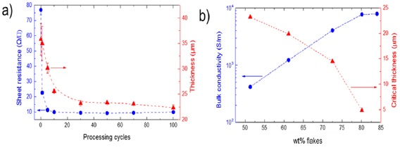
Figure II.7. (a) Rs and film thickness as a function of processing cycles for a formulation with 73 wt% flakes, (b) bulk and critical thickness as a function of loading (70 cycles). All samples are dried for 10 min at 100 °C. Reproduced from [178].
Download figure:
Standard image High-resolution imageII.2.2.4.2. Method 2: production of FLGs
Below we show that FLG can be obtained by adding an additional centrifugation step. Graphite powders (natural or synthetic) with D90 < 30 µm are mixed at a concentration 12 g l−1 with SDC at a concentration ~0.5 g l−1 in water and microfluidized for n typically <100). Following processing, samples are centrifuged typically at 10 000 rpm (17 000 g) for one hour. Films obtained by vacuum filtration of the FLG ink have Rs ~ 4.5 kΩ □−1 at 90 nm thickness, significantly better than the equivalent sonication produced graphene films that have Rs ~ 8.9 kΩ □−1 at 160 nm. The effects of processing cycles, pressure, surfactant concentration, centrifugation speed and graphite loading on graphene concentration are shown in figures II.8(a)–(f) AFM indicates that the exfoliated material consists of FLG, with ~18% SLG (figure II.9).
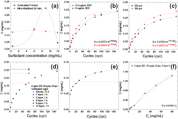
Figure II.8. (a) Effect of SDC concentration at fixed processing cycles (~60 cycles, 20 min, red) compared to sonication processing (9 h, black). (b) Effect of surfactant concentration 0.5 g l−1 (red) and 9 g l−1 (black) and process cycles. (c) Effect of process pressure 20 k psi (black) 30 k psi (red). (d) Effect of centrifugation parameters; (e) effect of using NaCMC as a stabilizer. Dashed red line represents sonication processing using the same NaCMC loading. (f) Effect of increased graphite loading.
Download figure:
Standard image High-resolution image
Figure II.9. (a) AFM height scans of flakes microfluidized for 20, 60 and 100 cycles. (b) Histogram showing the lateral size distribution of flakes with increasing process cycles. (c) Histogram showing the AFM height distribution for increasing process cycles.
Download figure:
Standard image High-resolution imageII.2.2.5. Ball milling
Ball milling can produce FLG at low-cost and under environmentally friendly conditions. It does not require solvents, avoiding the use of toxic organics, while increasing efficiency in terms of time and energy.
Two effects take place in ball milling [163]: the shear force, that promotes the synthesis of large-sized flakes, of the order of the starting graphite planes, and the vertical impacts applied by the balls during the rolling actions, which tend to deteriorate the flakes and must then be minimized in order to reduce the number of defects. Ref. [258] reported changes of graphite, during milling processes, through a nanocrystalline phase prior to amorphization. To avoid this and favour the shear force process, the use of solid exfoliating agents is recommended.
Exfoliating agents, including triazine derivatives, can be used to form multipoint interactions with the exfoliated flakes. Amounts around few grams of graphite and exfoliating agents, such as melamine (2,4,6-triamine-1,3,5-triazine), can be used to prepare FLGs, which can subsequently be dispersed in organic solvents, such as DMF or in aqueous media [179]. The lateral size of the resulting flakes can be modulated depending on the ball-milling conditions (atmosphere, revolutions, and time of treatment). Different triazine derivatives were tested, in relation to their ability to exfoliate graphite, not only experimentally but also by computational studies, which evidenced that melamine is a good option to favour exfoliation [259]. Melamine not only has an aromatic nucleus that can interact with the graphene π-system [259], but can also form an extended network on its surface, owing to the presence of hydrogen bonds (figure II.10). Melamine can then be washed away using hot water, leaving high quality graphene suspensions, with very small Raman D peak.
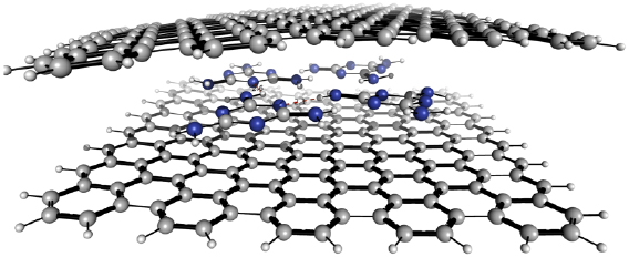
Figure II.10. Supramolecular assembly of melamine between SLG.
Download figure:
Standard image High-resolution imageIn a typical experiment, 7.5 mg of graphite and 22.5 mg of melamine are ball-milled at 100 rpm for 30 min, under air atmosphere, in a stainless steel grinding jar containing ten stainless steel balls of 1 cm of diameter. The resulting solid mixture is dispersed in 20 ml of solvent, obtaining black suspensions. Filtration can remove melamine from the suspensions, giving rise to FLG dispersions in different solvents. If DMF is used as a solvent, colloidally stable dispersions are obtained with no precipitate observed. If water is used as a solvent, a concentration gradient appears, and some precipitation takes place after stabilization of the dispersion, at room temperature, for 5 days.
When preparing dispersions in water, melamine can also be eliminated by dialysis, which is highly recommended, mainly because this technique allows keeping the flakes always in dispersion [213]. It is advisable to hand-shake the dialysis sack and to apply a pulse of mild (bath sonication for no more than 1 min) if any precipitate appears in the black dispersion during dialysis. Once melamine is removed, the black dispersion is kept in the stabilization container at room temperature for 5 days, in order to obtain a concentration gradient. The liquid fraction with stable sheets in suspension needs to be carefully extracted, avoiding the meniscus and the precipitate, in which non-exfoliated graphite remains. The obtained aqueous dispersions, with concentration ~0.1 g l−1, are stable at RT for a few weeks. According to elemental analysis, these dispersions contain an amount of melamine lower than 1 ppm, which is considered non toxic [260].
Characterization of the FLG shows a low number of defects, with Raman ~0.2–0.6, confirming that no oxidation occurs during the preparation [179]. In [261], ab initio calculations on graphene-melamine-water systems have been performed focusing on how small amounts of melamine molecules tune the adsorption of few water layers on SLG. These reveal that melamine acts as a non-covalent anchor, keeping some water molecules near SLG, providing a quantitative estimation of the non-covalent interactions (dispersion and hydrogen-bonding), which provide the required driving force to stabilize the SLG-water systems.
A further advantage is that the aqueous suspensions can be lyophilized after having been frozen [262]. A very soft and low-density black powder, consisting of FLGs, is produced this way. This solid can be safely stored and shipped, being easily dispersed in water, culture media or other solvents, using mild sonication combined with shaking with no change in its structure (figure II.11). The mass yield of the entire process, starting from graphite, is ~30%.

Figure II.11. FLG powder (left) and its dispersion in cell culture medium (right).
Download figure:
Standard image High-resolution imageIn [179], powders were characterized with elemental analysis (EA), TGA, XPS, TEM and Raman spectroscopy. EA resulted in average values ~94.3 wt%C, 0.4 wt%H, 0.4 wt%N and 4.9 wt%O [1728]. TGA showed a weight loss [1728], in agreement with EA, confirming the non-oxidative nature of the milling treatment. This feature was also corroborated by XPS [179], as deconvoluted plots confirmed the presence of small amounts of oxygenated groups, from the C 1s and O 1s core level spectra and traces of melamine. XPS spectra (figure II.12) indicate that 15 min ultrasonication does not add a significant number of defects. TEM was used to determine the lateral flake sizes [1729], concluding that FLG have a wide size distribution ~200–2000 nm.
Figure II.12. XPS spectrum of powders produced by ball-milling of graphite.
Download figure:
Standard image High-resolution imageThere is an increasing interest in the use of GRMs in biological applications. Dispersions in water and culture media allow the preparation of hydrogels for drug delivery [259], the study of synaptic functions in culture brain cells [263, 264] as well as environmental toxicity studies [262].
The addition of small amounts of solvent during milling was reported to improve exfoliation [153]. Solvent drop grinding was shown to be an effective technique to accelerate mechanochemical reactions [265]. The addition of catalytic amounts of a liquid phase facilitates molecular mobility, inducing reactivity in normally inactive systems. Therefore, wet milling conditions have been probed, and ball milling exfoliation of carbon nanofibers was reported [153]. Melamine was used as the exfoliating agent: 0.5 ml of solvent was added to 30 mg of nanofibres/melamine mixture. The Hansen solubility parameters of each material were studied in order to discriminate SLG from the rest of materials (FLG, poorly exfoliated carbon fibres and melamine) after the milling treatment. This allows one to select a suitable solvent to disperse mainly SLGs [153]. The quality of exfoliation was studied by Raman spectroscopy. Although there is a compromise between exfoliation quality and graphene concentration, these wet conditions follow the same trend established by the Hansen solubility parameters, permitting SLG dispersion [153].
To achieve larger particle sizes (in the range of microns), mechanical exfoliation by ball milling or high-shear mixing can be combined with chemical intercalation. Intercalating Li and ammonium-based ions (such as tetraethylammonium-Et4N+- ions) between layers weakens the van der Waal forces [266]. Ball milling supplies shear forces high enough to exfoliate the intercalated compounds. Using ionic liquid (IL) or ammonium based deep eutectic solvents as the milling liquid accelerates the kinetics of the intercalation because it increases the activity of ammonium ions [266]. Deep eutectic solvents are green solvents having the advantages of non-flammability [267], high thermal stability (>150 °C) [267], wide liquid phase range (usually over a range of 200 °C–500 °C) [268], negligible vapour pressure (<10 Pa at RT) [269] and easy recycling [270]. These properties eliminate the safety problems associated with typical organic solvents. An eutectic mixture of urea and choline chloride (2:1) can be produced by stirring the two components until clear liquid is formed. The liquid can be then charged into the grinding chamber with 2 g graphite, 4 g battery grade Li chips, and yttria stabilized zirconia milling media. The ball milling runs under a flow of N2 gas inside a glovebox. It is better to pause the grinding process for 30 min every 2 h to allow the system to cool. To recover the exfoliation product, the samples are then washed with DMSO, and centrifuged at 1500 rpm to remove thick flakes. The milling speed should be controlled to below 500 rpm to avoid extensive heating and to minimize defects in the produced flakes.
II.3. GO and RGO
II.3.1. GO
GO has a number of properties that are advantageous for applications. Due to its oxygenated surface, it can undergo complete exfoliation in water [271–275], yielding colloidal suspensions of individual sheets [273, 276, 277], that can be further functionalized, deoxygenated or dispersed in polymeric matrixes to give new multifunctional materials and composites [276]. This, combined with chemical tailoring [216, 217, 278] and biofunctionalization [279–283] makes GO a promising candidate for biomedical applications where water compatibility is crucial, e.g. in tissue engineering, drug delivery, cancer treatment and biosensing [281–289]. Unlike liquid-exfoliated LMs, GO is typically one layer thick [276]. This high surface to volume ratio and the mechanical strength lends itself to using GO as electrode material in energy storage and conversion [290, 291] or as filtration membrane for gas and ion separation [292, 293]. In addition, GO has some unique features. For example, unlike other LMs, it is amphiphilic, due to the non-uniform distribution of the various oxygen functional groups and can self-assemble into a range of nanostructures with different morphology at interfaces [294]. When increasing the concentration in dispersion, GO undergoes a phase transition from colloidal isotropic to nematic liquid crystalline phase, where the GO sheets are oriented in parallel [295]. The liquid crystalline phase leads to an enhanced alignment of GO sheets in those assembled structures, offering improved mechanical and electrical/thermal properties, compared to the random-oriented configuration of GOs which is important for electrochemical applications and opens up possible applications of GO in optical switches and photonic crystals [295].
GO can be prepared by oxidation of graphite using highly oxidant reactants such as H2SO4, KMnO4, H2O2 [156, 157]. The preparation method strongly influences the surface chemistry and related chemo-physical properties, ultimately affecting its functionalities. In 1859, Brodie first reported the synthesis of GO by adding potassium chlorate (KClO3) to a slurry of graphite in fuming nitric acid (HNO3) in a single portion [296]. In 1898, Staudenmaier improved Brodie's method by replacing ~two thirds of fuming HNO3 with concentrated H2SO4 and by adding KClO3 in multiple portions during the reaction, rather than in a single portion. Such modification had the same oxidation efficiency of reiterative Brodie oxidations (achieving high oxygen contents, up to C:O = 2:1) but in a single synthetic step. However, the Brodie and Staudenmaier method was not widely used because of the potential risk of explosions [297]. In 1958 Hummers and Offeman proposed a safer approach, currently widely adopted and known as Hummer's method [156], consisting of the replacement of KClO3 by KMnO4 and NaNO3 in concentrated H2SO4. Ref. [298] reported that excluding NaNO3, increasing KMnO4 and a mixture of H2SO4/H3PO4 can improve the oxidation process. In these conditions the reaction is not exothermic and no toxic gas is produced.
The method proposed in Refs. [272, 298] allows one to prepare highly soluble (>4 g l−1) water-soluble GO for studying the biological and toxicology effects on living cells [235, 286, 287]. In this way, GO sheets could be prepared with constant surface chemistry, but varying lateral size, spanning from 100 µm down to less than 100 nm [235]. The lateral size of the GO flakes after a typical oxidation can be tuned by sonicating the starting solutions for different times, from 0 to 100 h, in milliQ water (for a systematic study of GO size versus sonication time see Ref. [136]). GO can also be prepared by the Hummer's method directly on SiC wafers from graphene on SiC, with the property that the GO layers remain on the substrate for further surface studies and electronic devices production [299–301].
It is still not clear which are the most relevant factors regulating the interactions between GO and biological molecules, tissue structures and organisms. Numerous studies [235, 286, 287, 302] have shown that GO chemical purity, chemo-physical parameters and morphological properties can play a crucial role on cells viability and functionalities [302].
Taking advantage of the size tunability and high solubility of GO, the effect of the lateral size of GO in different biological systems was investigated for human and murine phagocytic cells [235], human intestinal cells [286], human lung and colon carcinoma cells [303], different enzymes of human [287] or bacterial [304] origin, gelatine membranes and fibres of animal origin [305].
In Ref. [235], three GO solutions, sonicated for 0, 2 and 26 h (with average lateral size ~1.3, 0.27 and 0.13 µm) were mixed with human monocyte macrophages (hMDM) and murine intraperitoneal macrophages (mIPM), revealing that the flake size has significant impact on different cellular parameters (i.e. cells viability, reactive oxygen species (ROS) generation and cellular activation, figure II.13). Ref. [235] reported a strong interaction (>90% internalization) with the cellular membrane, leading to the sliding of flakes under the membrane layer. GO samples could be internalized by both human and murine macrophages in a size-dependent manner. The more the lateral dimensions of GO were reduced, the higher were the cellular internalization and the effects on cellular functionality [235]. Flakes with the smallest lateral dimensions (<300 nm) were better internalized by primary macrophages. A 'mask effect' was observed due to the 2d shape of GO, with a preferential parallel orientation of the GO sheets onto to the cellular surface.

Figure II.13. (a)–(c) SEM image of GO solutions sonicated for different times, then spin coated on 300 nm SiO2/Si(1 0 0): 0 h-GO (a), 2 h-GO (b), and 26 h-GO (c). (d) Flake size distribution of the 0 h-GO, 2 h-GO and 26 h-GO samples from SEM statistics. (e) Optical map of mIPM cells incubated with GO. Red dots indicate where Raman spectra was taken to detect internalization of GO into the cell. Adapted from [238], with permission of The Royal Society of Chemistry.
Download figure:
Standard image High-resolution imageAn efficient an green electrochemical oxidation of graphite to GO was reported [306]. Compared to traditional GO synthesis, the process bears the advantage that it is scalable, fast (<30 min opposed to hundreds of hours) and the risk of explosions is minimized. While electrochemical exfoliation has been developed to synthesize GRM with minimal oxidation (see section II.5), it has previously not been used to prepare GO. The electrochemical GO production can be achieved in two sequential steps starting using flexible graphite paper as anode and Pt as a cathode. In the first step (typically 20 min), a stage-I GIC is formed in concentrated H2SO4. In the second step, diluted (50 wt%) H2SO4 is used as electrolyte and the GIC as anode. Within seconds, the intercalation compound is oxidized and exfoliated. The dispersion produced is then filtered and washed to remove sulfuric acid and then redispersed by bath sonication if desired. Due to the lower acid concentration in the exfoliation step compared to the traditional Hummer's method, the dispersion is less viscous facilitating the filtration and washing step. Importantly, the process can be designed in such a way that a continuous oxidation and exfoliation is achieved and the degree of oxidation is readily tuneable by the concentration of sulfuric acid. The most critical step is the choice if starting material, as neither graphite powders, not flakes or rods are suitable.
II.3.2. Reduction of GO
There is a growing and active investigation into the preparation and use of RGO due to its good electrical conductivity properties (from 10−5 S cm−1 to 1000 S cm−1, [307]), and increase in mechanical reinforcement of polymeric matrixes [308]. E.g., 0.2% RGO can improve from 25% to 50% the mechanical properties of epoxy matrix composites[309]. Whereas thermal, chemical and thermochemical reduction of graphene and GO are customizable and versatile methods for preparing different types of RGO, they show several problems that hamper the synthesis of defect–free SLG. Among them, there are difficulties in complete removal of functional groups and the restitution of morphological characteristics of the material prior to the oxidation and sonication processes. RGO is highly polydisperse [307] in the lateral size, from less than 1 µm to more than 100 µm, due to the distribution of crystal size in the starting natural or synthetic graphites, and also due to the scissor effect that breaks the graphenic planes during the oxidation and/or the sonication processes [310]. However, the RGO thickness is controlled by the exfoliation of GO [311] and, depending on the preparation method and conditions, 1L can be obtained [312]. One of the first isolation of graphene was realized by reduction of GO by hydrazine in 1962 [273, 274].
There are several key characteristics of RGO that should be considered and evaluated to obtain optimum performance for a particular application: average lateral size, thickness, C/O ratio, the quantification of other heteroatoms, and surface area. Lateral sizes >5–10 µm are not suitable for fiber reinforced composites by vacuum assisted liquid resin infusion, LRI, or resin transfer moulding (RTM), due to the difficult filtration of the RGO flakes by the fabrics during the processing [313]. Lateral sizes >30 µm produce low percolation threshold composites, as compared with medium (<20 µm) and small (<5 µm) ones, due to size of overlapped areas and the higher number of contacts between particles [314].
Thickness is also a key factor for the performance of RGO in applications. In photocatalytic applications of RGO-TiO2 the highest photocatalytic activity was observed with the SLG composites, and it decreased with N; this effect is attributed to higher charge carrier mobility and improved prevention of electron–hole pairs recombination [315]. Better results were obtained by co-exfoliation of graphite and TiO2 [1716]. In some composites, this effect is also observed [143], however, in most of the applications in composites, SLG is not needed.
The C/O ratio and the quantification of other heteroatoms are important factors to determine the range of applications suitable for RGO. RGO with high (10%) to medium or low (1%) content of O is not suitable for thermal conductive properties, and a decrease to the oxygen content to lower than 0.5%w and distances between defects >15 nm are needed [141]. Also, the sp2/sp3 ratio is relevant for energy applications [309], catalysis [316] and gas absorption [317]. In many applications, such as mechanical reinforcement of polymers, increase dispersion in composites or fire retardancy [318] and for further covalent functionalization, GO with 15%–25% O concentration is needed and ~8%–4% O are recomended.
Surface area is another of the key characteristics. The Brunauer–Emmett–Teller (BET) theory serves as the basis for an important analysis technique for the measurement of the specific surface area of materials. We will refer to those experimental methods as BET specific surface area, SBET, measurements. SBET is related to N and is a key factor enabling a material for energy applications. N can be estimated by dividing the maximum surface area of SLG, 2630 m2 g−1 by the specific surface determined experimentally by BET 2630/SBET, [319]. According to Ref. [320], RGO with SBET ~600–700 m2 g−1 are mostly SLG.
The density of RGOis another key parameter. GRMs with high SBET values produced by thermochemical reduction exhibit low densities, even lower than 4 g l−1 [311]. For some applications a compaction of the RGO for further processing is needed [321].
Many strategies exist for the chemical, thermal and thermochemical reduction of GO, which strongly depend on the process and conditions selected for the reduction process, and the final performance required. Toxic hydrazine, sodium borohydride, hydroquinone have been used [322], as well as 'green reducers' such as organic acids [323], alcohols [324] and local high T reduction [300]. Biochemical molecules [325], amino acids [325], natural extracts [325] or metals [326], and several approaches other have been proposed [327].
Hydroiodic acid, often in combination with other acids, has been suggested as potent and versatile reducing agent [328]. GO reduction can be carried out at low T either in solution or for GO films and papers, in the gas phase [328]. GO self-assembled on the air/water interface can also be efficiently reduced by hydroiodic acid [329]. When using hydroiodic acid on GO films, it was found that the strength and ductility of the film was improved [157]. Compared to other methods of thermal reduction, such as reduction with hydrazine or vitamin C, it was found that hydroiodic acid reduces the GO without causing additional damage to the lattice [328].
Based on reproducibility, post-processability and ease up-scaling, alcohols are ideally suited for chemical reduction [324]. GO is first dispersed in the selected alcohol. Concentrations of GO ~5–20 g l−1 should be used because, before the reflux of GO in alcohol, ultrasonication (of a batch or in a continuous system) is needed for the exfoliation from graphite oxide to and an increase of viscosity should be avoided. The higher the GO lateral size, the lower GO concentration should to be used, due to the lower stability of the GO in the suspension. The main disadvantage of this process is the high volume of alcohols needed. E.g., to process 100 g of GO, a 20 l vessel is needed. However, alcohols can be recycled by column distillation with recycling yields >95%. Critical parameters are the selection of the alcohol and the time under reflux. By using x-ray diffraction, the reduction can be monitored based in the decrease of the intensity of the (0 0 1) peak of GO and the presence of (0 0 2) peak of RGO [330].
The electrical conductivity of RGO is also dependent on the chemical reduction process [307]. A Longer reflux time in isopropyl alcohol (IPA) produces higher conductivity. However, after 15 h no significant improvements are observed, see figure II.14.

Figure II.14. Conductivity of RGO reduced in IPA reflux versus reduction time.
Download figure:
Standard image High-resolution imageAfter this reduction step, filtration of RGO at RT is required. This is easy to perform, due to the powdery aspect of the material. This can be air-dried or oven dried at less than 100 °C for 12 h. It is important to control the drying process to prevent contaminations, avoid thermal expansion and decrease density for further processing. High pressure and hydrothermal methods are more complex [331, 332], but efficient reduction of GO can be achieved, obtaining lower O concentration compared with traditional chemical reductors, such as hydrazine [332].
The products obtained from chemical reduction of exfoliated GO [307] have usually poor, <100 S cm−1, electrical properties due to the high O concentration (>10%) and the presence of structural defects [157, 158, 333].
RGO can be prepared by thermochemical methods as an alternative route for reduction of GO [311], where restoring the sp2 SLG structure is additionally achieved by thermal annealing [276]. Besides O removal by reduction, enhancing the graphitization by repairing the C–C sp2 π-bond network at defect regions during the reduction process [311] can further improve the electrical properties of exfoliated RGO, for electrical, thermal, and self-sensing applications.
For the preparation of RGO with <1% O, several strategies can be used, such as >1800 °C annealing T, long processing times (>60 min at 1500 °C), reducing atmospheres, such as H2, alcohols, hydrocarbons, etc. Thermochemical reduction can be done at medium 800 °C or high T (>1200 °C), depending on the final requirements. The choice of the working atmosphere has an impact on the final RGO characteristic, particularly on its O content. Thermal reduction can be done in vacuum [334] or inert atmosphere [311] in a reducing H2 environment [335] and using carbon donor molecules. Alcohols are very effective in the reduction of GO and the partial restoration of the graphitic structure due to their carbon donor characteristics. Other carbon donor molecules or a combination of hydrocarbons [336] are alternatives for the production RGO with O content <2% O at moderate T < 800 °C.
In thermochemical reduction, the working atmosphere comprises a gas carrier, which in most cases is an inert gas such as N2 or Ar, and the carbon donor/source molecule or combination of molecules. Ar is preferred as gas carrier over N2, due to the potential doping of with N RGO during the reduction process. For the restoration atmosphere, it is crucial to control the carbon donor and also the kinetics of the pyrolytic decomposition of the active gas. Carbon molecules result in the decomposition and formation of other non-graphene species and non-desired aromatic molecules [337]. Thus a low concentration, usually <5% is recommended. Significant improvement of the reduction process when compared to the material obtained in H2 was reported [338].The use of carbon donor atmospheres is the most cost-efficient to obtain highly reduced GO, with O concentration from 0.25% to 1%.
The reduction T determines the kinetics of the thermal decomposition (from 300 to 2000 °C), but a low cost- efficient reduction must be pursued in an industrial enviroment and the time and T of the process should be the lowest possible. Efficient processes at low T have been reported in [339], obtaining graphene for Li batteries at a low T ~ 300 °C in 5 min.
II.3.3. Aerogels based on RGO
Graphene flakes can be used as building blocks for the preparation of 3d low density structures, such as sponges, foams, hydro- or aerogels [340–346]. These materials exhibit a highly open structure, with interconnected hierarchical pores that enhance the accessibility to the whole surface of the material and improve ion diffusion. The assembly of the graphene sheets into macrostructures can also improve the mechanical properties, while retaining other properties associated to individual graphene layers [340, 341]. GO can be used for the preparation of composites with tailored macroporous structure through the assembly of GO sheets with different templates. After template removal, complex GO-based materials with hierarchical porosities can be prepared [347]. The combination of processing at RT and a subsequent treatment at moderate T allows the preparation of highly conductive bare carbonaceous electrodes [348] and composites, which may serve as self–standing electrodes for Li ion batteries [347].
Ice–templating [349] is a useful technique for the preparation of macroporous reduced graphene oxide-based aerogels (ARGO). Ice–templating involves the freezing of a GO suspension, then subsequently freeze-dried to sublime the ice crystals formed within the structure. This process is useful for the preparation of a variety of a homogeneous nanostructured composites, with application in energy storage, catalysis, sensing or separation [350], it offers a better control on the porosity of the resultant materials. The modification of parameters such as T or immersion rate, impacts the textural properties of the resultant material. Ice-templating also allows gives structures with hierarchical porosity, which can favor the transport and diffusion of molecules to the whole surface of the material, highly desired in adsorption processes for separation and purification purposes and catalytic applications, not only of soluble pollutants in waste waters, but also for immiscible substances in biphasic systems [1730]. In energy storage applications, ARGO was proposed as electrodes for supercapacitors, Li-ion, Na-ion or metal-air batteries [341].
Ice-templated ARGO have been investigated as self-standing electrodes for energy storage devices [351]. These structures can be assembled into the electrochemical cells without the need of binders, which do not contribute to the capacity of the electrode, but can decrease its conductivity and block the access of the electrolyte ions to the surface of the active materials. As anodes for Li ion batteries (LIBs), sp2 graphene not only improves the electrodes electronic conductivity, thus enhancing the power of the device, but it can also buffer the volume changes undergone by some active species used as high energy anodes for LIBs, during alloying with Li [352].
The processing of these materials as self-standing composites provides additional value to the electrodes since they can be directly mounted into flexible portable electronics [353].
II.3.4. Si-RGO and SnO2-RGO aerogels
ARGO composites can be prepared following the route schematized in figure II.15. First, an homogeneous suspension of GO, alone or in the presence of a certain precursor of the desired particles, is prepared. Second, the suspension is rapidly frozen by its immersion in liquid nitrogen. Then it is freeze-dried to remove the ice-crystals formed upon freezing, leaving the macroporous structured in the GO-based monoliths. Finally, samples are partially reduced by a thermal treatment conducted under inert atmosphere, yielding a macroporous carbonaceous network in which RGO sheets are decorated with crystalline particles.
The microstructure and porosity of the resultant aerogels can be tuned by changing rate and T of freezing. Fast freezing does not allow graphene layers to self-arrange with the ice crystals front, giving rise to materials containing macropores randomly distributed within the structure [354].
Figure II.15. Schematic representation of the route followed for the preparation of RGO composite aerogels.
Download figure:
Standard image High-resolution imageFigure II.16 shows photographs of different aerogels obtained by ice templating. In these cases, GO suspensions obtained by the sonication of graphite oxide by the Hummer's method were used [120]. For the synthesis of Sn-based ARGO composites an aqueous suspension was used, but in the case of Si-ARGO, the GO and the SiNPs were initially dispersed in ethanol. Homogeneous GO suspensions in the presence of the precursor are in this way obtained [352, 355]. Then, the suspension is frozen in liquid nitrogen, and subsequently freeze-dried to sublime the ice-crystals, leaving the macroporous structured monoliths. Finally, the samples undergo thermal treatment under inert atmosphere to reduce GO and to form the desired crystalline phase.
Figure II.16. Photographs of GO aerogels prepared form different suspensions: (a) GO (2 mg ml−1), (b) GO (6 mg ml−1), (c) Sn-GO and (b) RGO composite aerogel, obtained after thermal reduction of GO aerogels at 800 C.
Download figure:
Standard image High-resolution imageFor the preparation of the GO suspension in ethanol ~5 g l−1, an aqueous suspension of GO is washed several times with dry ethanol. The suspension is then sonicated and centrifuged to remove aggregates in the sediment. When mixing Si NPs and GO, the use of ethanol is justified, since Si-RGO composites generally need pre-oxidation of the Si NPs or ultrasonication, in order to improve their dispersibility in polar media, to be homogeneously mixed with GO [356, 357]. A highly homogeneous, see figure II.17, and stable dispersion of non-oxidized Si NPs was achieved in this way [355].

Figure II.17. Representative SEM images of (a) A-RGO, (b) A-Sn-RGO, (c) A-SnO2-RGO and (d) A-Si-RGO.
Download figure:
Standard image High-resolution imageSi-GO composites were prepared by mixing Si nanoparticles with the GO suspension in ethanol under inert atmosphere, then, solvent was reduced to 10% to be subsequently frozen and freeze-dried, to be then thermally reduced at 1000 ºC under dynamic Ar/H2 (95:5) atmosphere. The resulting material has large macropores in a highly open porous structure formed by graphitic flakes homogeneously decorated with Si NPs (~50 nm diameter), figure II.17(d).
This procedure also allows the in situ deposition of the particles on the surface of the graphene flakes. Sn and SnO2-ArGO, were prepared by dissolving SnSO4 in the GO suspension and the the pH was increased to 9 using NH3 solution. Then, the suspension was freeze dried to obtain macroporous Sn(OH)4–GO composites [352].
GO-based aerogels were thermally reduced under a dynamic argon flow to increase their electrical conductivity. Heating the samples under a dynamic argon flow, Sn-ARGO (figure II.17(b)) at 800 °C and SnO2-ARGO (figure II.17(c)) at 650 °C were obtained [352]. Figure II.17 shows a highly porous material formed by RGO flakes which contain large macroporous randomly distributed along the structure. In both samples, the Sn sub-micrometer particles showed a homogeneous distribution on the graphene sheets and a narrow particle size distribution, higher in the case of the metallic Sn particles (~750 nm diameter) than SnO2 particles (~250 nm diameter), ascribed to the carbothermal reduction, melting and re-crystallization of Sn particles [358] over 650 °C.
These aerogels have been processed as self-standing electrodes, without any binder nor metallic support, showing promising results as anodes in LIBs[347]. In the case of the SnO2-ARGO composites, reversible capacity of 1010 mAh  was measured at 0.05 A g−1 and 470 mAh
  at 2 A g−1, with reasonable Coulombic efficiencies (>98%) and stability after 150 charge–discharge cycles [355]. Si-ARGO electrodes showed reversible specific capacities ~700 mAh
  with associated Coulombic efficiencies >99% within 2–0.05 V. These electrodes also showed a good stability during 100 charge–discharge cycles [355]. This indicates that ARGO can accommodate volume changes of Si particles and, at the same time, improve the conductivity of the electrode without additives. Due to their high electronic conductivities and light weight, graphene aerogels are good candidates as support in the preparation of electrodes for next-generation Li batteries such as Metal-air batteries or Li-S batteries [359] or Li ion capacitors [360].
II.3.5. GO membranes
Membranes can be fabricated, e.g. by vacuum filtration, even though other deposition techniques can be used [1731]. GO membranes have gas and ion filtration properties [293] making GO an interesting material for water purification and desalination. Ref. [361] reported that GO based membranes are permeable to water, but hold back most other liquid and gases. Research in this area has been expanding with a range of review papers [293, 362–365]. A brief overview will be given here.
GO-based membranes are both selective and highly permeable to water, chemically and physically stable. However, fouling and biocompatibility still need to be addressed [362]. GO/FLG hybrid membranes were reported improved chemical resistance towards chlorine, and enhanced NaCl rejection (up to 85%) [366].
These GO material membranes can be described as an interlayer nanocapillary network, due to the connected interlayer spaces [365]. This network, together with the gaps between edges of non-interlocked neighboring GO sheets, and the cracks or holes of the GO sheet, provide passage for molecules or ions to permeate through the GO membrane in aqueous solutions so that effective separation of different molecules and ions can be achieved depending on the network morphology, degree of GO oxidation, lateral size, stacking in combination with size and chemical nature of molecules and ions. Molecules or ions with smaller hydrated radius, less charge and weaker interaction with GO sheets permeate through the GO membrane more easily than larger ones, driven by the high capillary-like pressure [365, 1731]. The separation performance at high water flux and rejection rates can be tuned by adjusting the GO sheet size, the thickness of the GO membrane, water pH, and the GO membrane structure as summarized in Ref. [365].
The key aspect of these type of membranes is the self-assembly of the flakes into well-ordered macroscopic laminates unlike in GRM-polymer composites, where the flakes are less ordered and less densely packed [363]. The flakes arrangement in the membrane is thus an important parameter influencing separation performance. This not only depends on the characteristics of the flakes themselves (size/thickness, degree of oxidation), but also on the deposition technique [367]. Highly ordered, interlocked GO flakes were obtained by building membranes by spin-coating a GO dispersion in a layer by layer fashion. These interlocked membranes showed better CO2/nitrogen selectivity than less ordered ones [363, 364]. For a more detailed discussion on transport mechanisms see Refs. [363, 364].
II.4. Chemical intercalation and reductive exfoliation
II.4.1. Graphene from GICs
The intercalation of graphite with sulfuric acid can be exploited for the production of GO. Graphite can also be intercalated by a number of other species to yield GIC [160]. The fabrication of donor-GIC after intercalation with, e.g. alkali metals, has gained increasing importance. Refs. [368–374] reported that such acceptor-GICs are very suitable precursors for covalent functionalization of graphene (see section VIII.1).
In typical covalent functionalization sequences, the negatively charged SLG first act as reductants for electrophiles (for example alkylhalide) [368], which are subsequently attacked by the intermediately generated organic radicals or H-atoms, yielding covalently modified graphene. This wet-chemical functionalization is facilitated by the fact that, due to Coulomb repulsion, the negatively charged graphenide [373] layers within the solid GICs can be dispersed in suitable organic solvents (see Ref [373] for more details).
One fundamental question is if whether all negative charges of the graphenide intermediates can be controlled or even completely removed in such redox reactions [376]. Only complete oxidation is expected to avoid reactions with moisture and O during workup [375], leading to side products with undesired and additional O and H functionalities. More importantly, the controlled removal of all negative charges from the solvent exfoliated graphenide intermediates with a suitable oxidation reagent allows for the bulk production of defect-free graphene. Ref. [375] reported that the treatment of K intercalated graphite with benzonitrile (PhCN) leads to discharging, i.e. taking away of the electrons from charged layers, of the individual graphenide sheets upon the formation of the colored radical anion PhCN.-, figure II.18, which can be used to monitor the accompanying exhaustive and Coulomb force-driven migration of K counterions from GICs into the surrounding benzonitrile phase. The suppression of reactions of dispersed graphenides with moisture and air takes place when no treatment with benzonitrile is provided, resulting in graphene. This represents a mild, scalable, and inexpensive method for wet-chemical graphene production. This reductive graphite exfoliation approach can be extended to water as solvent [377].
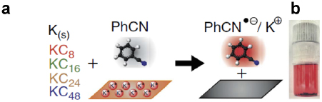
Figure II.18. (a) Reaction scheme for the quantitative electron transfer from various GICs to PhCN leading to dissolved K+ ions and the red coloured radical anion PhCN.-. (b) Photograph of a sealed vial containing KC8 in a concentration of 5.0 × 10⁻¹ M in PhCN.-, adapted from [375].
Download figure:
Standard image High-resolution imageII.4.2. Chemical exfoliation of transition metal dichalcogenides
LMs, such as TMDs, can be reductively exfoliated via intercalation compounds [159]. Typically, MoS2 is intercalated with n-Butyllithium (n-BuLi) in an inert solvent such as hexane [378]. In contrast to graphite, intercalated MoS2 does not react with water [378] so that this can be used for subsequent exfoliation.
Water is added to the reaction mixture to destroy excess BuLi. At the same time, gas formation occurs, which acts as driving force to expand MoS2 and individualize the layers. After further washing and centrifugation-based purification, a colloidally stable MoS2 dispersion in water can be obtained with negatively charged, predominantly 1L flakes (70%–90%). As a result of the negative charges, a phase transformation from the semiconducting 2H-MoS2 polytype to the metallic 1T polytype is observed. Such negatively charged MoS2 can be used as precursor for subsequent covalent functionalisation using electrophiles [379, 380]. Another approach, based on chlorosulfonic acid assisted exfoliation was developed, allowing to keep the original semiconducting properties of 2H-TMD (as MoS2 and WS2) [381, 1412, 1413, 1732, 1733].
This intercalation chemistry was explored in the 80s [159], but the interest was not in producing exfoliated flakes in a liquid dispersion. Ref. [379] studied the impact of intercalation conditions on the final product of chemically exfoliated MoS2. In a typical exfoliation of MoS2 with n-BuLi, the n-BuLi is used in ~10-fold excess. These reaction conditions can lead to the introduction of defects, as exemplified by a significant mass loss in TGA under inert conditions (figure II.19(a)). No specific mass fragments can be assigned to this weight loss, suggesting it is not the result of a well-defined surface derivatization [379]. The major mass fragment observed has a mass over charge (m/z) ~18 and was assigned to -OH groups, figure II.19(a). This disruption of the structure is not observed when MoS2 is used in excess over n-BuLi. The work-up is more tedious, with less material obtained as individualized flakes. After centrifugation, flakes with similar lateral dimensions and thickness distribution are produced (figure II.19(b)) suggesting that there is scope to optimize chemical exfoliation with respect to yield of 1L MoS2.
Figure II.19. Characterization of chemically exfoliated MoS2 with different intercalation conditions. (A) TGA weight loss of MoS2 and MoS2 chemically intercalated with excess of BuLi and MoS2. Bottom: mass profiles for m/z = 15–18 which constitute the main weight loss in chemically exfoliated MoS2 using excess BuLi. (B) AFM thickness histograms of MoS2 intercalated using excess MoS2 (top) and BuLi (bottom). Inset: representative images. Adapted from [379], copyright American Chemical Society.
Download figure:
Standard image High-resolution imageII.5. Electrochemical exfoliation
Graphite can be exfoliated to SLG and FLG by applying a bias in ionic aqueous (or organic) electrolytes [137, 382]. Electrochemical exfoliation (EE) requires one graphite electrode and a metallic counter electrode in conductive media, which is not equipment-intensive. The exfoliation completes in minutes to hours, producing gram-scale quantities of flakes with high Yw up to 80%. The graphene quality is tunable: sheet size, C/O ratio, solubility and electrical conductivity can be modified depending on the types of graphite precursors, electrolytes and operating potentials [383].
The selection of the graphite electrode is an important parameter. Various graphite precursors (including natural graphite and synthetic graphite), in the form of powder, foil, paper, rod, flake and plate, have been studied for electrochemical exfoliation [397, 1734]. From our perspective, graphite foil is considered as an ideal raw material due to the ease of operation, as well as good tolerance to the volume expansion during exfoliation.
II.5.1. Aqueous media
H2SO4 can be used to prepare GICs as the ionic diameter of sulfate ion (0.46 nm) is close to the interlayer spacing of graphite (0.33 nm), which is the prerequisite for efficient intercalation. Efficiency here relates to the degree of exfoliation, a higher ratio of MLG is considered more efficient than thicker flakes. In this way efficiency is related to the average thickness of the exfoliated platelets: the lower the thickness, the higher the efficiency. Dilute H2SO4 aqueous solutions were used [384, 385] to encourage graphite exfoliation because it is less corrosive. Ref. [385] immersed a graphite anode together with a counter electrode (Pt foil) into 0.1 M H2SO4The exfoliation started when a potential of 10 V was applied. This gave 80% 1-3LG with high exfoliation yield (60%) and high C/O ratio (12.3). Under electric current, the oxidation effect on graphene is strong, owing to the interplay between proton (H+) and sulfate ion at low pH. The oxidation effect is defined as the oxygen content in the exfoliated materials, which usually results from the attack of oxygen-containing radicals by water splitting [386]. Water electrolysis generates oxidative radicals (HO· and O·), which contains a collection of sulfate salts (e.g. sodium sulfate, ammonium sulfate, etc) instead of H2SO4 [387]. By doing so, Ref. [387] reported >85% of 1-3LG with dimensions up to 40 µm and C/O ~ 17.2, implying a low level of O functionalization. Another strategy to suppress oxidation is to remove radicals from water splitting [388]. A series of scavengers have been investigated. Ref. [388] reported 2,2,6,6-Tetramethyl-1-piperidinyloxy (TEMPO) to be the most effective, reaching C/O ~ 25.3, average sizes ~5–10 µm and hole mobility up to 405 cm2 V−1 s−1. Electrochemical exfoliation can produce not only graphene but also highly oxidized GO [306]. E.g., a two-step anodic oxidation in concentrated (98 wt%) and diluted (50 wt%) H sulfuric acid enables the synthesis of GO with C/O < 2 and high yield (95%) of 1L similar to those achieved by traditional Hummer's methods.
There are still several challenges: (1) the exfoliation only occurs at a single electrode (anode or cathode), limiting the production rate; (2) insufficient intercalation results in polydisperse flakes (with varying N), which requires additional separate procedures; (3) flakes trend to restack in solution, due to strong in-plane interaction when the stabilizers are absent, which needs careful selection of suitable electrolytes.
II.5.2. Non-aqueous media and molten salts
Another strategy to minimize O content is to use cathodic intercalation and O-free electrolytes [389]. The intercalation of small cations with graphite from organic solvents is the principle of many energy storage devices [389–393]. Graphene can be prepared by electrochemical intercalation of Li+ within the graphite interlayer space, followed by dissociation of the resultant intercalating compound using prolonged sonication. Ref. [394] tried to reduce the sonication time by intercalating graphite with Li, followed by a second intercalation of large tetra-n-butylammonium ions. In both cases, the strong decomposition reaction of the solvent cations hindered the formation of LiC6 and/or ammonia GICs. Therefore, another sonication step was need to completely detach the graphene flakes.
Graphite can be fully exfoliated via an electrochemical process in organic solvents without the need of sonication or an inert atmosphere, by using DMSO saturated with Li and small alkylammonium ions (triethylammonium, Et3NH+) [395]. An electrochemical program is used to apply a controlled cathodic potential on the graphite electrode, enabling the formation of exfoliated powder [266]. In a three-electrode system, a chronoamperometric step of −1.7 V on Ag/AgCl is applied for 5 min, followed by linear sweep voltammetry at a rate of 10 mV s−1. The potential is then kept at −5 V for 5 min, to allow intercalation of the electrolyte cations, finally it is swept linearly back to the open-circuit potential to decompose the resultant complex compound. During the first chronoamperometric and the second linear sweep voltammetry steps, solvated carbanion complexes are formed according to reactions II.1-5. The second chronoamperometric step at −5 V is important to complete the intercalation process. This intercalated compound could decompose cathodically if the potential is held at negative values according to reaction (6) or on the oxidation cycle according to 7. In both cases, dissociation of the intercalated compound is associated with Et3N gas formation, more likely taking place between the graphene layers, which applies more stress on SLGs and separate them further apart.


The intercalation from RT electrolytes is a slow process (diffusion coefficient <1.2 × 10⁻¹⁰ cm2 s−1) [396] and limited to few µm from the edge of the graphite grain [397]. Attempts to increase chemical activities of Li ions or other cations by using pure ILs or deep eutectic solvents did not overcome the kinetic barriers [398]. Hence, it is important to repeat the exfoliation process for more than one cycle to obtain a yield >70% the big flakes [389]. Another alternative is to use molten salts at T > 500 °C as the electrolyte. [399–401] developed for the exfoliation of graphite based on Li intercalation from molten LiCl electrolyte containing water. In a typical experiment, anhydrous LiCl powder, which serves as anode, is charged in a graphite crucible. The cathode is graphite. The cell is heated to ~800 °C, above the melting point of LiCl, and a stream of water is bubbled into the molten bath. Electrolysis is achieved by applying a constant direct current between cathode and anode. After allowing the cell to cool down to RT (Ar gas flow), graphene powder can be recovered from the solidified salt by washing with hot distilled water and vacuum filtering. Finally, the black powder is heated at 1300 °C under inert gas atmosphere containing hydrogen. The process demonstrates commercial viability and a molten salt volume ~10 L can produce ~4.5 kg flakes in a day [400, 402].
II.5.3. Combination of electrochemical and microwave expansion
Microwave (MW) irradiation is currently employed in many fields of organic synthesis to shorten reaction times, to enhance both reaction yields and product purity, to provide eco-sustainable synthetic methodologies, by replacing or reducing the use of polluting reagents [217]. Graphite can interact with the oscillating electrical field of MW radiation, giving high T gradients and increased reaction rates (e.g. for fast functionalization of GO) [217] as compared to conventional, procedures such as conventional chemical functionalization at RT in solution. Therefore, the T attainable using MW (>80 °C) can be applied to exfoliate graphite [217].
Electrochemistry can be used for a fast (<30 min) and massive (>70%w/w intercalated molecules/graphite) intercalation of suitable molecules, such as perchlorate ions, into graphite [217]. Degradation of these molecules in GICs is then triggered by MW irradiation, creating a gas pressure surge in graphite and yielding exfoliation [217].
Charged perchlorate ions could act as 'Trojan horses', to favour the intercalation of uncharged acetonitrile molecules [348]. These work as nanoscopic foaming agents, and decompose with MW irradiation to generate a pressure surge within graphite, resulting in exfoliation. The process yields soluble, monoatomic (52% SLG), large (72% of the sheets extending beyond 1 µm) GRM sheets characterized and then tested as transparent electrodes [348] and capacitors [348]. These electrodes can also be functionalized with nanoporous layers of inorganic oxides, after the pre-intercalation of electrolyte species (e.g., FeCl3–nitromethane electrolytes), to obtain, e.g. composite electrodes for LIB [1735].
Electrochemical treatment can be performed starting from HOPG as a working electrode and a Pt wire as a reference electrode. Ions such as sulfates and perchlorates can be efficiently intercalated into graphite, whereas intercalating uncharged molecules is more difficult [131], and can usually be achieved only by several hours sonication, with a lower yield (few%) of both exfoliated material and 1L. The exfoliation process works only if the surface energy of the intercalated organic liquid is similar to that of graphene [131]. The process is limited to high-boiling solvents (T > 100 °C), such as NMP or DMF. To overcome this challenge, Ref. [348] used perchlorate ions to promote the intercalation of an organic, uncharged molecule (acetonitrile), which was present in high excess, as a solvent. Graphite was intercalated and partially expanded by electrochemical insertion of ClO4- in acetonitrile by applying a + 5V for 0.5 h. In this way, negatively charged ClO4 − ions intercalated through grain boundaries or defect sites and favoured the penetration of the smaller, uncharged acetonitrile molecules. The fundamental role of ClO4 − was demonstrated in a comparison experiment by using acetonitrile alone, for which no intercalation was observed [348]. The amount of molecules intercalated into graphite was high (70% w/w), as estimated from TGA of the intercalated graphite electrode [348].
After electrochemical intercalation, MW irradiation expanded the graphite interlayers through decomposition and gas evolution of acetonitrile to yield a foam-like, multilayered powder [348]. The expansion was fast (~10 s) and yielded an increase in volume of the initial graphite ~600% [348]. The role of acetonitrile in the expansion was demonstrated in a comparison experiment, in which no expansion was observed for graphite treated only in aqueous solutions of HClO4 or NaClO4 without acetonitrile [348]. Figure II.20 shows a schematic of the process, and photographs of the material at the different processing stages.
Figure II.20. Illustrations of graphite after intercalation, expansion, electrochemical exfoliation and reduction steps (from left to right).Adapted from [348], © Wiley-VCH Verlag GmbH & Co. KGaA.
Download figure:
Standard image High-resolution imageII.6. Sonication-assisted versus chemical versus electrochemical exfoliation
Graphite can be exfoliated by different chemical methods in the liquid phase. One of the simplest approaches is ultrasonic treatment in organic solvents (see II.2). Some dipolar aprotic solvents (e.g. DMF, NMP) or surfactants in aqueous solutions are effective to stabilize graphene in solution without re-aggregation [131].
A more effective, but disruptive, approach to solubilize graphene is covalent modification, in particular by the formation of GO (see Section II.3). In presence of strong oxidants, the aromatic carbon network is oxidized with the creation of hydroxyl, carboxyl and epoxy moieties. The hydrophilic nature of these moieties on GO facilitates solution processing of concentrated 1L on different substrates substrates (>60% 1L[277]). The GO flakes can be then reduced to give electrically conductive RGO. However, numerous defects on GO are not fully restored after reduction and the electronic properties of RGO are poorer compared to pristine graphene.
Another more controllable, slightly less disruptive approach to exfoliate graphite takes advantage of electrochemistry (see Section II.4). By adjusting the applied potential in suitable electrolytes, graphite electrodes can be either negatively or positively intercalated to obtain GICs, and then exfoliated by solvent decomposition directly during electrochemical treatment or by further thermal treatment.
The most common LPE methods are compared: sonication in solvent, chemical oxidation, and electrochemical oxidation. By using a graphite crystal as starting material, it was possible to study the structure of both the exfoliated and the non-exfoliated fractions on the nanometric and mesoscopic scale [137].
Figure II.21 shows AFM images of graphite basal surfaces that are left behind after different exfoliation processes. Exfoliation by sonication in DMF proceeds layer-by-layer. Only the upper part of the HOPG is interested, and the process is slow, requiring several hours to alter the substrate roughness [137]. CE is the most damaging treatment for HOPG, destroying significantly the crystalline layer through deformation and intercalation. The obtained sheets are mostly 1L soluble, tending to re-stack in a uniform LM. EEproceeds by mechanical expansion due to gas formation. Whole areas of the substrate rise up due to gas formation, tearing apart the superficial layers and removing large amounts of material. EE works on a larger scale, oxidizing the upper HOPG layers, with more cracking and swelling on the macroscopic scale. Damage to HOPG is proportional to the applied bias, with disruption of crystalline stacking. Exfoliation is fast and more efficient than in solvent, yielding 1-2L GO > 50%, with tunable oxidation.
The differences between the three methods highlight the trade-off between speed and efficiency of exfoliation on one side, and preservation of material quality on the other.
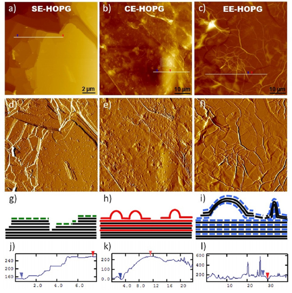
Figure II.21. AFM images of HOPG basal surface after treatment by (a) sonication-assisted, (b) chemical exfoliation, (c) electrochemical exfoliation. Z-range: (a) 400 nm, (b) 600 nm, (c) 1 µm. (d)–(f) gradient-filtered version of each image. (g)–(j) Schematic representation of the structure of the HOPG substrate after exfoliation procedures. (j)–(l) Height profiles taken along the lines shown in (a)–(c). From [137], © Wiley-VCH Verlag GmbH & Co. KGaA.
Download figure:
Standard image High-resolution imageII.7. Computational modelling of exfoliation of LMs
The rush towards innovative applications has stimulated the synthesis and exfoliation of novel LMs. Graphene, BN, TMDs, and BP are nothing but the tip of the iceberg of a rapidly increasing LM family. To keep up with this experimental thrust, it is of uttermost importance to expand the portfolio of potential LMs. In this respect, first-principles simulations offer unprecedented opportunities to predict and design novel LMs [403, 404] providing new directions for experimental explorations. To achieve this computational synthesis of novel LMs, two main strategies have been put forward, that mirror the bottom-up or top-down techniques of experiments.
Top-down approaches consist in systematically exploring databases of known experimental compounds, looking for LMs that can be exfoliated into 1L. This requires first to recognize if a parent bulk 3d crystal structure results from the stacking of chemically disconnected components. Geometrical algorithms based on the comparison between interatomic distances and van der Waals or covalent radii can be adopted to assess the chemical connectivity between units. The dimensionality of each unit can then be estimated, leading in particular to the identification of 1L. Ref. [405]data-mined subset of structures with low packing ratio from the Inorganic Crystal Structure Database (ICSD) and identified 92 LMs, nearly half of which had never been discussed before. More recently, this portfolio has been significantly enriched by Refs. [406, 407], who not only extended the investigation to other databases (including the Materials Project database and the Crystallographic Open Database), but also validated their results against accurate van-der-Waals density-functional-theory calculations of the binding energy. This led to the discovery of 681 [406] and 1825 [407] exfoliable LMs that will provide a rich portfolio of candidates to explore for optimal electronic, optical, catalytic, topological, and magnetic properties. E.g. instance, a new magnetic LM, Fe3GeTe2, has been already found [408] among these new exfoliable structures [406], but many more promising candidates await discovery. This approach has been adopted not only to collate these extensive databases [1737–1740] but also as a one-shot effort to find novel LMs from bulk layered compounds; e.g. for arsenene and antimonene [409] or 1L Hittorf's phosphorus [410].
Novel LMs materials have also been 'synthesized' computationally through bottom-up approaches, starting directly with some chemical intuition. In this regard, a first possibility is to consider structural prototypes of known LMs and create hypothetical new structures by substituting elements with chemically similar species [403]. This led, e.g. to the theoretical prediction of germanene and silicene [411] by looking for stable Ge- and Si-based analogues of graphene. A list of 171 TMDs and oxides with favorable formation energies has been obtained by decorating the so-called H and T structural phases with 27 different transition metals [412, 413]. Ref. [414] extended this approach to other classes of materials including halides, semimetal monochalcogenides and atomically thin 1Ls, identifying 146 hypothetical LMs for which the electronic and magnetic properties have been computed [1736]. Another promising way to theoretically synthesize new LMs bottom up relies on global optimization techniques. Starting from a given set of elements, the ground-state structure is obtained by searching for the most stable atomic configuration and (possibly) stoichiometry using either evolutionary [415–417] or particle swarm optimization [418, 419] algorithms. These methods have been adopted for instance to predict 1L materials with no bulk layered counterpart, like SiS [420] novel phases of InP [417] and several 2d allotropes of boron [416, 421], known as borophenes. In the latter case, statistical methods based on cluster expansion have been put forward and predicted the structure of borophene on metallic substrates in agreement with experiments [422]. Figure II.22 provides a classification of LMs as easily exfoliable, potentially exfoliable, or with high binding energy.
Figure II.22. (a) Binding energy versus relative difference in interlayer distance predicted by vdW (DF2-C09) or non-vdW (revPBE) functionals. Materials classified as easily exfoliable, potentially exfoliable, or with high binding energy are colored differently. Well-known LMs are highlighted in the plot. Adapted from [407], © Springer Nature. (b) Calculated heat of formation for 216 1L-TMDs in the 2H and 1T phases. Oxides have the highest stability, followed by sulfides, selenides, and tellurides, in that order. The stability decreases as the metal ion goes through the transition-metal series. Adapted from [412], copyright American Chemical Society. (c) Examples of patterns predicted for free-standing 1L B polymorphs, from close-packed triangular, honeycomb. The numbers at the bottom right of each model mark the hole density, S1 and S2 are the observed phases. Adapted from [423], © Springer Nature.
Download figure:
Standard image High-resolution imageIII. Processing of dispersions
III.1. Size selection
III.1.1. Sedimentation-based separation
The exfoliation of LMs usually results in a heterogeneous dispersion of flakes having different morphology, i.e. lateral size and thickness [166]. There are many methods for the selection and processing of flakes [115, 131, 183–185, 424, 425] by means of ultrasonication [115, 131, 174, 183–185, 204, 424–427], shear mixing [176, 177, 238, 428–430], ball milling [179, 431–436], microfluidization [178], and wet-jet milling [437–440]. Centrifugation based size selection methods can be classified into sedimentation based-separation (SBS) and density gradient ultracentrifugation (DGU) [195]. Materials subjected to SBS are sorted on the basis of different sedimentation rates in response to a centrifugal force. Owing to its ease in handling, SBS is the most commonly applied size selection technique for GRMs. Typically, small and thin flakes are separated from larger, thicker counterparts. However, achievable size distributions are still rather broad except for the smallest and thinnest flakes. To tackle this, a number of variations to traditional single step SBS have been developed, such as band sedimentation [185] and liquid cascade centrifugation [186]. Different to SBS, DGU exploits the movement of the dispersed object to the point in the centrifuge tube where the buoyant density of the material matches that of the surrounding liquid. The addition of density gradient media to the mixture is typically required to adjust the density of the liquid to the higher density material [168]. As such, DGU has the potential to separate flakes by thickness, but is more challenging to perform than SBS. In the following sections we will discuss these different strategies, highlighting pros and cons.
III.1.2. Single step sedimentation
The SBS process is widely used to separate materials of different nature and morphology ranging from metallic nanoparticles (MNPs) [441], CNTs [442–445], to GRM flakes [115, 131, 174, 177, 183–185, 204, 238, 424–428, 430]. A theoretical description of the sedimentation process can be found in Ref. [195]. In brief, three forces act on the objects during the centrifugation, which determine their sedimentation rate (see figure III.1(left)): (I) the centrifugal force Fc = m2Dω2r, which is proportional to the mass of flake itself (mGRM), to the square of the angular velocity (ω), and to the distance from the rotational axes (r), (II) the buoyant force Fb = −mS 2r, which is linked with the Archimedes' principle, being proportional to the mass of the displaced solvent (mS) times the centrifugal acceleration, and (III) the frictional force Ff = −fv, i.e. the force acting on the GRM flakes moving with a sedimentation velocity (ν) in the solvent. Ff is proportional to the friction coefficient (f ) between solvent and the GRM flake. f depends on both physical parameters of the dispersed flakes, i.e. lateral size and thickness, and physico-chemical properties of the solvent they are dispersed in, i.e. the viscosity (η). Both parameters have a strong influence on the value of f .
Overall, the sedimentation of GRM flakes depends on their mass and frictional coefficient, which is shape dependent [115, 166, 424]. In first approximation, thick and large GRM flakes, having larger mass with respect to small and thin flakes, sediment faster with respect to the latter, since these have smaller mass. This allows to separate GRM flakes with different morphology [166, 424], see figure III.1. However, it is challenging to isolate large and thin flakes. The definition of large/thick and small/thin depends on the material that is used in combination with the centrifugal acceleration and the medium. This will be detailed further down below for a few examples.

Figure III.1. Sorting of GRM flakes by ultracentrifugation. The SBS approach allows separating thin and small lateral sized flakes (supernatant) from thicker and larger ones, which precipitate at the bottom of the ultracentrifuge tube as pellet. The final flake Dimensions (lateral size, final flake N) depend on the centrifugal acceleration, material and medium.
Download figure:
Standard image High-resolution imageThus, taking into account the dependence of the physical dimensions of the flakes on the centrifugal acceleration (expressed as relative centrifugal field, RCF, in units of the earth's gravitational field, g), it is possible to exploit SBS to prepare GRM flakes of different morphology. In a typical experiment, a dispersion is centrifuged at a fixed g-for a given time. Supernatant and sediment are then separated. The sediment contains larger and thicker flakes than the supernatant. By changing the centrifugal acceleration and centrifugation time, the flake sizes can be adjusted. E.g. the flakes in the supernatant will be smaller after centrifugation at higher accelerations or longer times. Any centrifuge (benchtop or ultracentrifuge) with either fixed angle rotor or swinging bucket rotors can be used.
Even though it is not required that the centrifugation is run for several hours until an equilibrium is reached, i.e. all flakes that will sediment at a given centrifugal acceleration have reached the bottom of the vial, it is recommended not to use centrifugation times shorter than 30 min. When centrifugation times are short, a steeper size/thickness gradient is formed in the vial. As a result, the size and thickness distributions in supernatant and sediment will depend on how the sample is decanted, leading to poor reproducibility. Centrifugation times ~1–3 h are recommended and lead to reproducible results. This also depends on the rotor and vial size, hence the distance the flakes need to travel to reach the bottom [246]. Often sediments are then discarded and supernatants collected for analysis and/or further processing. However this makes it a wasteful process.
With SBS, it has been possible to prepare samples having lateral sizes ranging from few nm to a few µm, both for FLG [131, 176, 184, 424–427, 446, 447] and other LMs [174, 185, 244, 425, 448, 449]. In terms of thickness, dispersions with SLG content up to ~60% were demonstrated in an SDC based aqueous dispersion [446], while ~33% SLG was reported for dispersion in NMP [447]. Such 1L-rich dispersions from SBS also contain predominantly laterally very small (<50 nm) flakes [446, 447]. Apart from the difference in percentage of SLG, the flakes processed in water-surfactant dispersions are, on average, also smaller (~200 nm) [184, 427, 446] with respect to NMP (~1 µm) [131, 447]. This difference is related to the difference in the viscosity of the solvents. When comparing the most widely used solvents (NMP and water where, with the addition of surfactant, the viscosity decreases) the viscosity of NMP (1.7 mPa s) [450] is significantly higher than water (~1 mPa s) [451]. A higher solvent viscosity increases the frictional force [195], reducing the sedimentation velocity [195]. Therefore, when using similar centrifugation conditions (centrifugation time and centrifugal acceleration), the flakes retained in the supernatant will be larger/thicker in higher viscosity solvents.
SBS also suffers from the further disadvantage that all flakes(also small < 50 nm) remain in the supernatant when operating at the low centrifugal acceleration (<1000 g) used to isolate large (µm) flakes. Hence, dispersions containing larger flakes on average are significantly more polydisperse and show broad size (20-few µm) and thickness (1–20 layers) distributions. This can be partially overcome by a band sedimentation approach, where the dispersion is placed on top of a solvent race layer (without flakes) prior to centrifugation [185]. E.g. a dispersion containing flakes in an aqueous surfactant can be onto a race layer of deuterated water containing the same surfactant [185]. During centrifugation, the flakes spread throughout the vial according to their sedimentation rate, related to their size. The centrifugation is stopped before the dispersion constituents reach the bottom of the vial, allowing for a collection of various fractions in one run. Smaller/thinner flakes remain closer to the top and are thus efficiently isolated from larger/thicker ones, closer to the bottom. This was demonstrated for MoS2 [185]. In this case, centrifugation at 1500 g for 10 min yielded various fractions ranging from mean lateral sizes of 350 nm and arithmetic mean N~15 in fractions close to the bottom, to 40 nm and 2L in fractions extracted from the top of the vial. Compared to traditional homogeneous SBS, the distribution histograms were narrower, i.e. the standard distribution was reduced by ~2 [185].
Even though this approach can be advantageous when various fractions with narrower thickness distributions than SBS are required, it suffers from a few disadvantages. First, the material quantity that can be processed in a single step is lower because it is beneficial to keep the sample layer thin, so that most of the volume in the cuvette is taken up by the race layer. Second, the final size-selected sample is diluted during the process, making high concentrations inaccessible. Third, a swinging-bucket rotor is required, as a fixed-angle rotor will not lead to such a defined movement of flakes through the race layer. Therefore, liquid cascade centrifugation (LC) has been suggested as versatile alternative to the above mentioned single step SBS.
III.1.3. Liquid cascade centrifugation
LCC is versatile and can be carried out using benchtop centrifuges [186]. This is a multi-step procedure, whereby various cascades can be designed according to the desired outcome. To demonstrate this process, a general cascade is portrayed in figure III.2. It involves multiple centrifugation steps, each with a higher centrifugal acceleration [186]. After each step the sediment is retained and the supernatant is then used in the proceeding stage. As a result, each sediment contains flakes in a given size range, 'trapped' between two centrifugation stages with different speeds. Similar to band sedimentation, small/thin flakes are removed from dispersions with predominantly larger/thicker flakes. As with traditional SBS, the lateral dimensions and N obtained depend on the design of the cascade (centrifugal accelerations), starting material and solvent. A few examples of lateral sizes and thicknesses are summarised in table III.1.
Figure III.2. Schematic representation of liquid cascade centrifugation. Adapted from [186], copyright American Chemical Society.
Download figure:
Standard image High-resolution imageCritical to LCC, the resulting sediment can be redispersed by mild agitation (shaking, or <5 min bath sonication) in the respective medium, enabling one to reach any desired flake concentration, as well as modification of the concentration of additives (such as polymers or surfactants). Virtually no material is wasted in LCC, resulting in the collection of larger masses of size-selected flakes from a single dispersion compared to homogeneous SBS, where the sediments are discarded. The procedure was thus found to be ideal to study size effects in applications [452]. It was applied to WS2 and MoS2 [186, 245, 452, 453] as Ni(OH)2 [240], GaS [188], BP [190] and FLG [176, 236] in solvents [176, 188, 190] as well as aqueous surfactant [177, 186, 236, 240, 452] or polymer systems [453]. Due to its versatility and the large accessible quantities, other reports adopted the procedure [454, 455]. Typical mean lateral sizes and N are given in table III.1 for a range of materials.
Table III.1. Overview of mean lateral sizes using LCC. For each material, the 'large/thick' and 'small/thin' fractions are defined by the midpoint of the centrifugation boundaries (given as central g). Data includes centrifugation in solvents (NMP, IPA) and aqueous SC solution.
| FLG SC [236] | FLG NMP [176] | WS2 SC [245] | MoS2 SC [245] | BP NMP [190] | GaS IPA [188] | |||||||
|---|---|---|---|---|---|---|---|---|---|---|---|---|
| Central g | 550 | 21 000 | 80 | 1800 | 0.33 | 7500 | 0.33 | 9900 | 690 | 17 500 | 170 | 850 |
| (nm) | 360 | 90 | 1000 | 160 | 170 | 35 | 270 | 55 | 615 | 150 | 450 | 100 |
| 8.1 | 3.3 | Not determined | 7.5 | 2.1 | 7.4 | 2.4 | Not determined | 29.5 | 11 | |||
From this table it is clear, that the outcome of the size selection depends on the centrifugal accelerations, the density of the material and medium. A deeper understanding and systematic analysis will enable the prediction of the outcome of the size selection. In any case, to achieve efficient size selection, it is critical to remove the supernatant from the sediment as completely as possible. This also means that for this procedure to work, the centrifugation time has to be long enough to allow the majority of the flakes to sediment to the bottom of the vial. This does not require centrifugation to equilibrium (unlike DGU). One can obtain a good separation of supernatant and pellet-like sediment after 2 h of centrifugation, when the filling height of the dispersion in the vial is <10 cm. Centrifugation times should be extended if greater filling heights are used [246].
The chosen size-selection cascade can be modified readily to suit a desired outcome. While this specific procedure yields flakes sizes and thicknesses over a broad size range in the different fractions, if only specific sizes are targeted, some centrifugation steps can be skipped. E.g. if medium-sized flakes are desired, the sample can be centrifuged at only two different centrifugal accelerations and the sediment redispersed. In first approximation, flake size selection occurs by mass in such a standard cascade, still making it difficult to select large (µm), thin (1–3 L) flakes like in homogeneous SBS. However, a design of secondary cascades [186] involving a combination of long (14 h), low-speed centrifugations (~1/5 of the lower g-boundary of the initial trapping) to remove thicker material and short (60 min), high-speed centrifugations (above the higher g-boundary of the initial trapping) to remove very small (10–20 nm) flakes has shown potential to overcome this limitation yielding a ~75% 1L (mean N ~1.3) with an average lateral size ~40 nm in the case of WS2 [186].
III.1.3.1. Density gradient centrifugation
The key disadvantage of the SBS process, not allowing one to isolate a high percentage (>10%) of 1L flakes of reasonable lateral size (>100 nm), can be overcome with the exploitation of DGU. This enables control on N, when flakes are subjected to ultracentrifugation in a preformed DGM.
Two approaches can be exploited for the separation of GRM flakes: isopycnic [456] and rate zonal separation [456]. Isopycnic separation allows spatial separation inside the cuvette of GRM flakes depending only on their buoyant density. This is defined as the density of the medium at the corresponding isopycnic point and is measured in g cm−3. GRM flakes, during isopycnic separation, move along the cuvette, until they reach the corresponding isopycnic point, i.e. the point where their buoyant density matches that of the surrounding DGM [457]. Hence, in principle, flakes should be sorted according to N. However, it is nonetheless difficult to obtain dispersions of exclusively large (micron-sized) 1L-GRMs. This is likely related to the fact that micron-sized SLG is a minority fraction in LPE samples. Hence, even if all SLG flakes are isolated from the dispersion, the average lateral size will still be in the range of hundreds nm.
For isopycnic separation, the choice of DGM is fundamental. Salts (e.g. sodium chloride, cesium chloride, and lithium chloride), sucrose, and iodixanol are the most widely used DGMs [458, 459]. The use of salts has some issues. First, they induce aggregation on the hydrophobic solutes [460, 461] which may negatively affect the sorting process. Second, density gradients produced with salts are less stable with respect to those using sucrose and iodixanol, due to their lower viscosity [462]. Sucrose suffers the opposite problem: it has high viscosity, which further increases exponentially at high concentrations [463]. Iodixanol seems to be better suited, due to density tuneability, with respect to sucrose, and higher viscosity compared to salts.
The effectiveness of the isopycnic separation is also strongly determined by the type of density profile of the DGM and its variation. During centrifugation the density profile redistributes as the DGM responds to the centrifugal force, resulting in a steeper gradient over time [464]. The density profile of the DGM can be: linear, nonlinear, or step [465, 466]. Linear gradients are used when the materials to be sorted have small (<0.05 g cm−3) buoyant density differences. For this reason, linear gradients can sort surfactant-micelle encapsulated CNTs with very small buoyant density difference, such as (6,5) (1.06 g cm−3) and (7,5) (1.08 g cm−3) dispersed in SC [467–469]. In nonlinear gradients, the DGM density changes nonlinearly along the cuvette and the density gradient is established during the ultracentrifugation process [465]. Nonlinear gradients are particularly suited to sediment particles over the entire length of the cuvette [465]. By exploiting nonlinear gradients, a variety of depth-density profiles can be produced according to the density variation. This allows the trapping of particles of different densities along the cuvette's length. Step gradients, formed by stacking layers of different density, are usually employed when the materials to be separated have larger difference in density (>0.1 g cm−3) [470]. The sharp variation in density at the interface of two different layers stops materials with a density smaller than the denser layer, letting the larger density ones pass through [470].
For separating GRM flakes, the problem is that these materials have high densities, with no intrinsically different density with N (e.g. MoS2, ρ = 5.06 g cm−3, WS2, ρ = 7.5 g cm−3, WSe2, ρ = 9.32 g cm−3), except for the surfactant shell, making this an important aspect of DGU. This fact makes the sorting of inorganic GRM flakes challenging in common DGM, such as iodixanol, with ρ = 1.32 g cm−1 [115, 469]. Therefore, in order to separate flakes by N, it is important to ensure that they have uniform surfactant/polymer coverage [183, 446]. This requirement is crucial, because the surfactant/polymer layer also contributes to the buoyant density of the entire system, thus resulting in slight variations of the buoyant densities of 1L- and FL- flakes, which can lead to isopycnic separation. This results in a spatial separation inside the cuvette, overcoming the limitations of conventional ultracentrifugation in a density constant medium.
A successful GRM flakes sorting by isopycnic separation mainly depends on the following: (1) a large as possible amount of 1L-and FL- flakes in the starting dispersions. Differences in buoyant density can be correlated to specific thickness (1L, 2L, 3L) only if individualized GRM flakes are encapsulated by the surfactant micelles or polymer molecules. This also implies the folding and wrinkling of the flakes will be problematic. (2) Uniform flakes coverage. This is ruled by the adsorption of surfactant or polymer molecules, and their aggregation, which can lead to clusters formation (i.e. aggregates of several molecules around the flakes basal plane). The effectiveness of the isopycnic separation is demonstrated by the yield of SLG to date, ~80% [183] with SC as surfactant or N separation of GO [471].
Isopycnic separation was also used to sort inorganic LMs [168]. One of the main issues is their high density. Thus, surfactant molecules, such as SC [469] cannot reduce their buoyant density sufficiently to match the density of the gradient. By using Pluronic F68, a greater hydration shell than SC is formed. This procedure allows to reduce the buoyant density of the encapsulated LMs [472, 473]. Pluronic F68 allows to reduce the buoyant density of BN [473] as well as TMDs such as WS2, WSe2, MoS2, and MoSe2 [472], within the limit of the DGM allowing for isopycnic N separation.
Another approach to sort inorganic LMs via isopycnic separation relies on the mixing of two DGMs [474]. The addition of cesium chloride to iodixanol, determines an increase of the maximum buoyant density supported by the DGM (i.e. 1.56 g cm−3) to the point where even high-density rhenium disulfide can be sorted layer-by-layer [474]. The addition of salts as DGM is not compatible with dispersions based on ionic surfactants, as these will crash due to charge screening.
Isopycnic DGU-based separation allows one to sort GRM flakes by thickness and lateral size, rather than mass, unlike SBS. However, DGU separation, although widely used in biology [195] and successfully applied to GRMs [168], has the drawback of being a process involving multiple iterations and, as such, it is time-consuming. Another issue for the further processing of the sorted flakes, i.e. ink formulation, is linked with the presence of the DGM in the dispersion, that may be problematic for processing and/or its removal.
Another methodology to sort GRMs in a centrifugal field is rate zonal separation (RZS) [457, 475]. In RZS, the ultracentrifugation is stopped during the transient centrifugal regime, i.e. before the materials under ultracentrifugation reach their isopycnic points [475]. RZS exploits differences in the sedimentation coefficient of particles under ultracentrifugation. Therefore, particles with different sedimentation coefficients will move along the cuvette at different sedimentation velocities [457, 475], determining their spatial separation [441, 475]. RZS was used to separate GO flakes with different lateral size [476], exploiting the fact that the larger is the flake lateral size, the larger is the sedimentation coefficient. RZS was also used for the lateral size selection of BP flakes [425]. Similar to DGU, a downside of RZS is that usually an ultracentrifuge is used (rather than a benchtop centrifuge) and that a DGM is added to slow down the sedimentation and lead to a more gradual distribution along the cuvette, which has to be removed prior to further processing. This contrasts to band sedimentation [185] as discussed above.
III.2. Inks formulation
The production of GRM flakes in dispersion following exfoliation and sorting finds a direct use for applications, such as in polymer composites. In many other cases, the as-prepared dispersion cannot be used directly. For applications requiring coating and printing, the dispersion needs a formulation process to obtain an ink. The composition of functional inks is linked with the target deposition/printing process [166], see table III.2. There are deposition/coating approaches where the ink formulation is not stringent, depending on the nature of the solvent used for exfoliation and sorting, the deposition can be carried out directly with the as-prepared dispersion. This is the case for vacuum filtration and transfer, spray and drop casting, where the most critical parameter is the morphology control of the dispersed flakes. For other printing processes, such as flexographic, gravure, slot-die and ink-jet printing, the formulation of the ink is more complex, requiring the addition of many components in pre-defined steps. In the following, a few examples are given.
Table III.2. Specifications to consider for different printing methods.
| Printing method | Viscosity | Layer thickness | Feature size | Registration | Throughput |
|---|---|---|---|---|---|
| [Pa s] | [µm] | [µm] | [µm] | [m2 s−1] | |
| Gravure printing | 0.05–0.2 [477] | 0.8–8 [477] | 75 [481] | >10 [481] | 60 [481] |
| <0.1 [478–480] | 3–30 [482] | ||||
| Flexography printing | 0.05–0.5 [477] | 0.8–2.5 [477] | 80 [481] | <200 [481] | 10 [481] |
| 3–30 [482] | |||||
| Offset printing | 30–100 [477] | 0.5–2 [477] | 10–50 [481] | >10 [481] | 5–30 [481] |
| 5–50 [483] | 3–30 [482] | ||||
| Screen printing | 0.5–50 [477] | 3–15 [477] | 20–100 [481] | >25 [481] | 2–3 [481] |
| 0.015 [484] | |||||
| 30–100 [481] | |||||
III.2.1. Tuning of rheological properties
The control of the ink rheology is key to ensure consistency and reproducibility. This is usually achieved by studying flow and deformation of the materials under external perturbation [485]. The complex structure of the ink determines a rheological behavior which is typical of non-Newtonian flow [486]. Thus, there is a non-linear relation between shear rate  shear stress (τ), and apparent viscosity η (ηapp = σ
 ) which depend on
  (or τ). This behavior is different from Newtonian liquids, where η = σ
 [487]. The shear rate determines the η behavior of inks and, thus, their range of application. Depending on their flow behavior, there are different classifications for non-Newtonian inks [488]: dilatant where ηapp increases with increasing
  [488], pseudoplastic, where ηapp decreases with increasing
  [488], and thixotropic, where ηapp decreases with time under a constant deformation and will start to rebuild once the shear force ηapp is removed [488], figure III.3. The ink rheology is strongly influenced by the GRM volume fraction, φ, with their shape and spatial arrangement [489], GRM flakes dispersed in a liquid affect its flow field resulting in an increase in energy dissipation due to fluid-flake and/or flake-flake interactions [489, 490]. These interactions increase with φ, restricting the flakes diffusion into small 'domains', formed by the nearest neighbors and η diverges. However, a theoretical model to predict η of fluids with dispersed GRMs does not exist yet. Such model is not even available for NPs in general, although a significant research effort has been carried out [491–493].
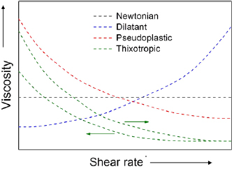
Figure III.3. Newtonian and non-Newtonian flow behavior of functional inks. Adapted from [166], © Wiley-VCH Verlag GmbH & Co. KGaA.
Download figure:
Standard image High-resolution imageWe now discuss the main ink requirements and the state of the art of the formulation for the of GRM-based inks for the main deposition/printing techniques.
Coating approaches, such as drop and spin coating, do not require a structured ink formulation, and, usually, the as-prepared dispersion can be directly deposited onto the target substrates. On the contrary, although the ink for spray coating deposition does not require a high viscosity, the aerosol formation and the subsequent drying process need the control of several processing parameters [494] such as viscosity [495], flow rate [496], and the distance substrate/spray-nozzle [497]. The nature of the solvent, which determines its evaporation rate at the substrate surface [496], is also a critical point for a uniform deposition. The solvent vapor pressure is crucial. Solvents having low vapor pressure, such as NMP (0.5mm Hg @25 °C), one of the most common for LPE of graphite [164], promote long crystal formation time [496]. This allows a consistent structural arrangement prior to the transition to the solid phase of the deposited feature [496]. On the contrary, high vapor pressure solvents, such as, e.g. isopropyl alcohol (IPA, 33mm Hg @25 °C) and toluene (24 mm Hg @25 °C), promote faster solvent evaporation [1741]. This subsequently reduces the ability of the flakes to organize in a ordered manner. The consequence will be a decrease of the final device performance, such as, e.g. a reduction of the charge carriers mobility in FETs [496]. Other sources of instability for the coating are linked with the geometry of the spray coating system, i.e. small nozzle size, or the jetting pressure, i.e. low pressures reduce the flow rate, which produce scattered droplets on the substrate and eventually a non-uniform coating [496]. A continuous coating is obtained by high deposition rates [145, 496]. The uniformity of the coating is also determined by the appropriate substrate/nozzle distance [497]. If this too short, the ink previously deposited onto the substrate can be blown away by the incoming flow. If it is large, the solvent can evaporate during the flight time, i.e. before the droplets reach the substrate.
The formulation of the ink for an inkjet process requires the control and tuning of various liquid properties such as ρ, η, and γ [498], which are then summarized in the following dimensionless figures of merit (FOM): the Reynolds (NRe) and Weber (NWe) [499, 500] and the inverse of the Ohnesorge number, Z (1/NOh) [500]. The Z number is independent on the drop velocity (m · s−1) and it is the most used FOM for inkjet printing [501–507]. Different Z values have been proposed, ranging from 1 to 91 with different functional materials [501–507].
Other parameters for the ink formulation have to be considered, such as, e.g. the physical dimensions of the flakes dispersed in the ink, that can agglomerate and clogg the print-head. Usually, it is required that flakes have lateral sizes smaller than ~1/50 of the nozzle diameter [508] (typically ~100 µm [509]). Other parameters to be optimized for the printing/deposition process are wetting and adhesion [510] to the substrate, as well as the distance between nozzle and substrate (typically 1–3 mm) [511].
An even more structured inkis needed for flexography and gravure printing. Although both require a high viscosity ink, there are several differences [166]. In flexography, there is a plate with a raised surface that spreads the ink onto the target substrate. Gravure is an intaglio process, where the ink is first transferred onto an image carrier and then printed on the target substrate. As summarised in table III.2 and Ref. [166], gravure printing is usually faster (~1000 m min−1) than flexo (~500 m min−1), with printed stripes thicker (~1 µm in gravure) than in flexography (<1 µm). The viscosity is also different: in flexography this is in the 50–500 mPa · s range, while in gravure it is higher 100–1000 mPa · s.
GRM-based inks for flexography and gravure were formulated [512, 513]. Ref. [512] reported a flexography ink by using CMC as a binder for FLG flakes in a water/isopropanol solution, obtaining a η ~20 mPa · s. The as-formulated ink was printed onto a flexible ITO substrate at 0.4 m s−1, and used as counter electrode for the realization of a flexible dye-sensitized solar cell (DSSC) [512]. A FLG/terpineol ink (η ~0.2–3 Pa · s from the homogeneous dispersion of FLG-ethyl cellulose powder (5–10 wt%) in a mixture of ethanol/terpineol (2.5:1 volume%) was reported in Ref. [513]. For the formulation of high viscosity GRM-based inks, there are several issues to be addressed. First, the solvents used in LPE (e.g. NMP) are toxic and have very low η (<2 mPa · s). The use of alternatives such as volatile alcohols, e.g. ethanol [513] and isopropanol [512], is against the current environmental regulations, requiring the minimization of volatile organic compounds [514]. Second, the GRM concentration in these solvents is low (<1 g l−1). Thus, in order to produce a functional (e.g. conductive) film, many print passes are required. The increase of GRM fillers could determine a problem with the solvent evaporation and in-series printability. In this context, the use of high boiling point solvents requires post-processing annealing for solvent removal [515], thus posing limitations on target substrate.
By increasing η, it is possible to obtain a paste, needed for screen printing. FLG-based conductive-pastes (i.e. FLG [516], RGO [517–519] and flakes [520, 521]) are emerging as possible alternatives to those based on metal NPs.
A paste based on FLG powder dispersed in terpineol, with ethylcellulose as a binder was prepared in [516]. The paste contained flakes at a concentration of ~80 g l−1, having a η up to ~10 Pa·s at a shear rate of 10 s−1. The as-deposited paste required a thermal treatment at 300 °C for 30 min to remove ethylcellulose. Another FLG-based paste, having shear thinning behaviour, was discussed in Ref. [522], which a gelation approach starting from the dispersion of expanded graphite in methyl ether dipropylene glycol in the presence of polyvinyl acetate and polyvinylpyrrolidone acting as binders. However, many parameters still need to be optimized for the development of optimal GRM-based inks/pastes for screen printing.
Figure III.4 shows a selection of polymers at 1 wt% loading that can be added to water or 50:50 water/ethanol solutions to modify the rheology. Polymers such as polyvinylpyrrolidone (PVP) can be added, with increased viscosity with increasing molecular weight (MW). Celluloses which are commonly used, provide high viscosity at low loadings, and impart thixotropic behaviour. E.g. aqueous FLG-based inks produced by microfluidization [178] have FLG loading >100 g l−1 and are formulated using 1 wt% sodium carboxymethylcellulose (NaCMC) to provide η up to 1800 mPa · s.
Figure III.4. Rheology modifiers in 50:50 water/ethanol solution at 1 wt% loading.
Download figure:
Standard image High-resolution imageNaCMC is not easily dissolved and its preparation can be affected by factors including the NaCMC particle size, rotational speed of the mixer, the rate at which solutes are introduced, and the solution T [523]. Heating the FLG dispersion should be avoided as this may promote flocculation. NaCMC is water-absorbent and has high water retention, therefore it clumps. To prevent this, NaCMC is added until dissolved completely and stirred to avoid bubbles. Bubbles and clumps need to be removed prior to printing.
The rheological properties of inks were investigated by monitoring the elastic modulus G'[J m−3 = Pa] [524], representing the elastic behavior of the material and a measure of the energy density stored under a shear process [524], and the loss modulus G''[J m−3 = Pa] [524], representing the viscous behavior and a measure of the energy density lost during a shear process due to friction and internal motions [524]. Flow curves measured by increasing  from 1 to 1000 s−1 at a gap of 0.5 mm, because this
  range is applied during screen printing. Figure III.5(a) plots the steady state viscosity of an ink produced from microfluidization (100 cycles) containing 73 wt% flakes as a function of
  . NaCMC imparts a drop in viscosity under shearing, from 570 mPa · s at 100 s−1 to 140 mPa · s at 1000 s−1. This is thixotropic [525], since the viscosity reduces with
  .
.
This behavior is shown by some non-Newtonian fluids, such as polymer solutions [526] and biological fluids [527]. It is caused by the disentanglement of polymer coils or increased orientation of polymer coils in the direction of the flow. In contrast, in Newtonian liquids, the viscosity does not change with  [527]. Refs. [528, 529] reported that thixotropy in NaCMC solutions arises from the presence of unsubstituted (free) OH groups. Thixotropy decreases as the number of OH groups increases [528, 529]. Figure III.5(b) plots the viscosity at hundred s−1 as a function of wt%FLG flakes (70 microfluidic process cycles). The NaCMC polymer (10 g l−1 in water) has a µ ~0.56 Pa · s at hundred s−1, and drops to 0.43 Pa · s with the addition of 5 wt% flakes. The loading wt% of flakes affects
  , which increases at 51 wt% and reaches 0.6 Pa · s at 80 wt.%.
Figure III.5. (a) Viscosity as a function of shear rate for an ink with 73 wt% flakes, (b) viscosity at 100 s1 for different wt% of FLG flakes. Reproduced from [178].
Download figure:
Standard image High-resolution imageIII.2.2. Hybrid inks
III.2.2.1. Graphene/polymer blends
We describe the formulation of a FLG-polymer-fullerene ink that can be processed by spin-coating to fabricate bulk heterojunction (BHJ) solar cells. The goal is to improve BHJ solar cells performance in terms of hole mobility, photocurrent efficiency and photoresponsivity [530]. Spin coating is commonly used to fabricate BHJ solar cells, allowing rapid deposition of thin films (~hundreds nm thickness) of different materials. In contrast to other printing techniques, it does not have any requirements in term of surface tension, viscosity, solute concentration and particle size for the ink to be deposited. Viscosity, volatility and concentration will affect the morphology and the thickness of the final film, which can be adjusted by tuning the angular velocity and the time of processing. The main advantages of spin coating are also the low amount of material required (µl) and the reproducibility of the film features for fixed working parameters.
Ref. [530] produced a FLG dispersion in 1,2-dichlorobenzene (ODCB) due to its compatibility with P3HT:PCBM by sonication and subsequent centrifugation to remove unexfoliated graphite. For the P3HT:PCBM dispersion, 10 g l−1 P3HT and 8 g l−1 PCBM are dissolved in ODCB and mixed with the FLG-ODCB supernatant. The P3HT:PCBM:FLG is then spin-coated on the substrate, which is a stack of glass, 100 nm ITO and PEDOT:PSS also deposited by spin coating. The BHJ solar cell is finalised by depositing a counter electrode of 20 nm Ca and 60 nm Al by evaporation. The critical step of the process is the mixing of the P3HT:PCBM to the ODCB-FLG supernatant, since the addition of the P3HT:PCBM could cause the destabilisation and flocculation of the ink. To prevent this destabilisation, the P3HT:PCBM should be added gradually and the dispersion immediately stirred after mixing. It is also important to not add an excess amount of FLG. In Ref. [530], only 2 wt%FLG is added; further increases cause aggregation of the FLG sheets, having a deleterious effect on exciton generation and charge separation/transport in the active layer.
III.2.2.2. Graphene/CNT films
Transparent conductive films (TCFs) on flexible substrates require homogeneity, optical transparency and stability under mechanical stress. Composites of graphene and CNTs are promising in this regard. In this framework the deposition of films by rod coating [531] fulfils the above-mentioned requirements. The use of the so-called Meyer bar allows deposition at RT and is fully scalable over large areas. The diameter of the wound wire of the bar determines the size of the grooves and controls the thickness of the liquid film, as well as giving alignment to the material improving the percolation. The key parameters of the ink to ensure a homogenous coating are viscosity ~1 mPa · s and a small contact angle ~20–30° [532]. The speed of the deposition can affect the homogeneity creating aggregates. Aggregates can also arise from a fast drying of the liquid film.
In addition to published work [1742], we found that a suitable ink can be prepared by bath sonicating (9 h) natural graphite (0.1 g l−1) in aqueous Triton X-100 (0.01 g l−1) followed by centrifugation (10 000 rpm) to remove the unexfoliated flakes. A CNT dispersion was prepared by tip sonication (2 h) P3-SWNT powder (Carbon Solutions, Inc.) in 1.8 g l−1 aqueous Triton X-100 followed by centrifugation (25 000 rpm). These CNTs were purified with nitric acid, and left in highly functionalized form containing 1.0–3.0 atomic% carboxylic acid moieties which can be derivatized with a variety of functional groups [1743]. TCFs can then be conveniently fabricated on various flexible substrates such as PET, PEN etc by rod coating. Typically, for a 10 × 10 cm2 substrate, 80 µl CNT ink is deposited and spread uniformly on the substrate using the Meyer bar. The wet film is allowed to dry in air before coating another layer. To remove the surfactant, after 2–3 coatings, the substrate is soaked in water-ethanol (50:50 in volume) solution at 60 °C and dried with nitrogen. The washing steps help to improve the final TCF conductivity. The same procedure is applied for the deposition of the FLG ink on the CNT film. Generally, for a 10 × 10 cm2 PET film, 40 repetitions of both inks are required to get to tens of kΩ □−1 at 80% transparency.
We find that these coatings can be applied in the fabrication of CNTs/FLG films as pixel electrodes directly on the backplane of an electrophoretic display. The CNT/FLG ratio is 40:60% in mass, assuring the uniformity of the film avoiding any aggregation. After every 3 coatings the film is washed to remove surfactants. For a 4 × 4 inch2 backplane, 150 ml of the water-ethanol solution (50:50 in volume) are used.
III.2.2.3. Inks with conductive polymers
In order to overcome the obstacles of efficient micro-supercapacitors (MSCs) manufacturing, such as scalability, high cost, and flexibility, new strategies based on processing of FLG nanocomposite inks are appealing. Direct printing/transfer techniques, including spray deposition, inkjet printing, and filtration, offer a promising protocol for production of MSC arrays, which can be processed onto both plastic and paper substrates at low T and over large areas. As a key component for these techniques, the selected ink should be stable, low cost, and easily printable on appropriate substrates; it should display excellent electrical properties without the need for aggressive post-treatments. High quality FLG obtained from electrochemical exfoliation could meet the above requirements.
Two inks were developed based on electrochemically exfoliated FLG (EEG) and conductive polymers [533, 534]. In one, conducting polymers, such as PEDOT:PSS, are mechanically mixed (bath sonication and stirring) with EEG in isopropanol [533]. The other is a EEG/polyaniline (PANI) composite ink [534], based on in situ polymerization of aniline in the presence of EEG. First, EEG is prepared and dispersed in DMF at the concentration of 2 g l−1, followed by noncovalent functionalization with 1-pyrenesulfonic acid sodium salt to obtain water dispersion of EEG. Then the EEG/DMF dispersion is blended with aqueous aniline hydrochloride and gently stirred or sonicated. Afterwards, ammonium persulfate is added, followed by a vigorous stirring (10 000 rpm, 6 h) to form uniform dispersion of EEG/PANI. After washing through ultra-centrifugation with water and ethanol for 3 times, the composite is dispersed in ethylene glycol to get a stable EEG/PANI ink [534].
III.3. Printing and deposition of inks
To develop applications that make use of LPE GRMs, it is necessary to convert the dispersed material into structures suitable for further studies. In general, flakes may either be deposited on a supporting substrate (such as glass, metal foil, Si, or plastic film) or act as a filler within some host material (such as polymers, metals or other nanomaterials) to produce free-standing composites. To this end, numerous liquid-phase processing techniques have been developed for the deposition of GRM dispersions in combination with other dispersed nanomaterials or polymers. Here, we outline some approaches used to produce a range of GRM-containing structures and devices such as vacuum filtration, spray coating, ink-jet and screen printing.
III.3.1. Vacuum filtration
Vacuum filtration is a simple technique whereby a GRM dispersion can be filtered through an underlying porous membrane to obtain nm-to-several micron thick films [535, 536]. These can be removed from the underlying support to produce a freestanding film, or transferred to rigid and flexible substrates and the porous membrane removed e.g. by chemical dissolution [536]. Although this technique may be unsuitable for the production of GRM-containing structures for commercial purposes, its low cost and its simplicity makes it ideal for research purposes. The main advantage is the possibility to wash away surfactants and solvent residues that usually affect the performance (e.g. conductivity) of the final films. Films with different thicknesses and composition can be produced by tuning the amount of dispersion, the pore size of the membrane and the vacuum pressure. GRM dispersions can be filtered on to various membranes, selected based on their pore size and chemical compatibility. Membrane types include cellulose, polycarbonate, anodized alumina, PVDF or PTFE. This allows to produce composites such as layered oxides combined with SWNTs for supercapacitor electrodes [239, 537], and TMDs/SWNT composites for electrocatalysis [452, 538] can readily be fabricated.
A wide range of filtration membranes are available with different surface chemistries and pore-sizes, the choice of which depends on the nature of the dispersion media, the size of the dispersed materials to be filtered and the desired approach to carry out film transfer. As the flakes produced by LPE often have lateral dimensions in 10s-hundreds nm, it is often necessary to use filtration membranes with the smallest possible pore diameters. Mixed cellulose membranes with 25 nm pore size are compatible with aqueous/surfactant dispersion media and can be subsequently dissolved using acetone to achieve transfer of the filtered film.
FLG films with thickness ~150 nm, transmittance ~50%, roughness ~8 nm and Rs ~ 1–2 kΩ sq−1 were prepared as conductive electrodes for biological applications [432]. These were also exploited in photonic applications, demonstrating sub-50 fs compressed pulses from a FLG-mode locked fiber laser [539], power scaling lasers [540], and monolithic waveguide lasers [541]. To produce these, a 25 mm diameter membrane filtration setup was used. 500 µl of dispersion with concentration ~0.1 g l−1 was diluted in 1 ml DI water. The dilution is necessary when the amount of the filtered dispersion is less than 1 ml to ensure uniform coverage of the membrane. If the dispersion has a high surfactant concentration, the presence of foam on the liquid surface has to be avoided before vacuum filtration. FLG is filtered through a 100 nm pore-size nitrocellulose (NC) filter membranes (Millipore). In order to remove the residual surfactant, the film on the membrane can be rinsed by filtration of 20 ml DI water. The filtering process requires ~2 h, which will increase with the film thickness prepared.
These films can be transferred on to glass coverslips (25 mm diameter) using the following procedure: 1. the FLG/NC membrane is cut to the size required and soaked in deionized water. 2. The FLG/NC is placed on the glass substrate with the FLG side face down. 3. A sheet of cleanroom paper is pressed by hand on the back of the NC to remove the excess water and trapped air between the film and glass. This is a critical step, as trapped air can leave some FLG non-transferred and, therefore, holes or fractures in the final film. The substrate is then clamped with two bulldog clips between two glass slides (30 × 30 mm). 4. The sample is left to dry in an oven for ~2 h at 90 °C. 5. The glass slides are removed and the coverslip left to soak in a covered beaker of acetone to dissolve the NC (at least 24 h) then soaked in isopropyl alcohol (1 h) and in deionized water (1 h). 6. The final FLG/glass sample is then dried in an oven for 2 h at 90 °C. Transfer on flexible substrates can be done with the same procedure. For improved transfer it is possible to use a hydraulic press in step 3.
Another method to make large free-standing membranes is electrophoretic deposition [542]. A suspension of GO with a concentration of 3 mg ml−1 is prepared and used as the electrolyte. Two identical pieces of well-polished Cu sheets (30 × 50 × 2 mm) are used as anode and cathode. A constant current of 2 mA is applied between the two electrodes for 2 min. The anode coated with GO is then dried under vacuum overnight, and then the free-standing GO membrane can be peeled off.
III.3.2. Inkjet printing
The printing of FLG inks is an attractive approach for developing electronic applications, such as transparent conductive films, printed electrodes and sensors. Inkjet printing is the ideal tool to produce prototype electronic devices at the lab scale. Indeed, it enables high resolution (~25 µm) of the pattern associated with the possibility of easily changing the pattern and the printed material. Several examples of inkjet printing of nanomaterials have been reported [201, 447, 543, 544]. In order to have a good jettability an ink has to satisfy particular requirements on Z, γ ρ, η and nozzle diameter. If Z is in the 4–14 range, satellite droplets recombine before reaching the substrate, but Ref. [447] demonstrated the possibility of having good printing also outside this range. Most lab-scale inkjet printers equipped with disposable cartridges, (e.g. Fujilm Dimatix 2800, Ceradrop X, LP50) mount cartridges with 50 µm diameter, so the flakes dispersed in the ink have to be at least 1/20 of the nozzle diameter to avoid printing instability and nozzle clogging. Dispersions produced by LPE followed by centrifugation are particularly suitable for inkjet printing, since they contain flakes with lateral sizes <2–3 µm [164]. Inks made by electrochemical exfoliation contain larger flakes even after centrifugation. These should be filtered before printing.
Inkjet printing can be performed on a variety of rigid (glass, Si/SiO2) and flexible (PET, PEN, PI) substrates. However, the wettability of ink droplets, defined by the contact angle, varies significantly. The most common procedures for changing the surface properties is to reduce the contact angle (improve wettability) by treating substrates. To increase contact angles, the substrate can be silanized by spin coating hexamethyldisilazane (HMDS) (40 s at 1000 rpm, followed by annealing at 80 °C for 2 min) [447]. Silanization requires surface hydroxyl groups to bind to. For flexible substrates, a preliminary UV ozone or oxygen plasma treatment will help to generate surface oxides. This results in more confined droplets, less spreading of the ink and higher resolution [447].
Flexible substrates already optimized for inkjet can be found on the market i.e. glossy papers, Novele (PET/SiO2/PVA) [545], etc which allow the quick wicking away of solvent, reducing the coffee ring effect thanks to their porosity.
Below, we report different examples for the production of strain sensors on flexible substrates from inkjet-pronted FLG. A flexible integrated platform, with four linear strain gauges 3 mm × 20 mm and a central Wheastone bridge strain gauge of 1.5 cm × 1.5 cm was printed on Novele substrate. A FLG-NMP ink with a concentration ~1 g l−1 and FLG flakes lateral size up to 600 nm was printed for 50 printing passes with an interdrop distance ~27 µm, inter-layer delay time ~ 120 s, and printer platform T ~60 °C. Annealing was performed at 80 °C in vacuum overnight. The strain gauges with a resistance ~100 kΩ show had gauge factor(GF ~20 at 25 mm bending radius with a change in resistance ~5% after 1000 bending cycles. FLG-based strain gauges with similar properties were printed on planarized PEN using a FLG-ethanol ink (2 g l−1) to make fully flexible wearable devices. The sensors are aligned with the proximal inter-phalangeal joints of the first and second digit of the hand, allowing the extension-flexion movements of these digits to be monitored. 20 printing passes, 22 µm inter drop distance and RT were used with an additional annealing at 80 °C in vacuum for 2 h.
With aqueous-surfactant based inks, one problem is the formation of foam bubbles following agitation of the print-head. This is observed at surfactant concentrations >6 g l−1. The presence of non-conductive species (surfactants, polymers) in the resulting printed films will reduce FLG network connectivity and, thus, conductivity. The ability for microfluidic processing to stabilize FLG at low surfactant concentrations (0.5 g l−1) meant foaming does not occur. The suitability of 0.5 g l−1 SDC stabilized FLG inks after 20 process cycles and centrifuged at 10 krpm, 1 h can be tested for inkjet printing (figure III.6(6)). Serpentine-type FLG resistors are printed on to photo quality paper (HP Advanced) at room temperature using an interdrop distance of 18 µm, with 20, 40 and 80 printing passes (figure III.6(b)). Prints are left to dry at RT for 60 s between passes. Although minimum optimization is required, prints with over 20 layers suffer bleeding, due to insufficient drying time, and nozzles could become partially clogged. During printing, the head is cleaned by an automated Spit-Purge-Spit cycle every 180 s. Patterns are printed for 20 passes at a time and the nozzles wiped by hand with IPA prior to printing more layers. After 20, 40 and 80 passes the resistance of the patterns decreases from~220, to 31, 3.7 MΩ, respectively, over ~40 mm (track width ~0.9 mm) as shown in figure III.6(b). The resistance response of these devices is tested with strain (3-point bending) and in different gas environments.

Figure III.6. Inkjet printing of microfluidized ink after 20 process cycles. (a) Typical jetting behaviour showing good droplet formation and the absence of satellite droplets. (b) Printed serpentine-type resistors after 20, 40 and 80 passes. (c) Resistance change whilst 3-point bending of three devices under tensile and compressive strain.
Download figure:
Standard image High-resolution imageThree-point bending is performed with a 300 N/2 kN Deben vertical three point tensile stage. The samples are bent with an extension rate of 0.5 mm min−1 and measured under tension (positive strain) and compression (negative strain), to a maximum of 5 mm displacement. The electrical resistance of the printed strain gauge varies, depending on the amount of axial bending strain in the device. Printed structures at 20 and 40 passes show very similar resistance versus strain curves (figure III.6(c)) with significant response to +0.4% strain (ΔR ~ +35%) and −0.4% strain ΔR ~ −25%). The 80 printed pass sample show significantly lower response (ΔR ~ ±10%) in line with the higher sample thickness. These changes are a result of conductivity variations, due to changes in length, as well as the distance between flakes. The relative change in electrical resistance (ΔR/R0) is related to the mechanical strain (ε) by the gauge factor (G = (ΔR/R0)/ε). These are 93, 85 and 39 for the 20, 40 and 80 print pass samples, respectively and thus comparable to other FLG devices produced by drop-casting or spray coating (G: 75–150 at 0.2% strain) [546]. These gauge factors are higher than graphite-based ink strain sensors (G: 19.3 ± 1.4) [547], and considerably higher than conventional strain gauges [548] or inkjet-printed metal strain gauges [549] in which GFactor ~ 2.
In addition we used inkjet printing to print heterostructure devices by placing one material on top of the other. Inkjet printed MoS2/FLG photodetectors (PDs) using LPE inks were demonstrated on PET. The devices were fabricated using a Dimatix 2800. A 40 µm MoS2 channel contacted by two inkjet printed FLG electrodes on top. 100 passes of both FLG and MoS2/NMP based inks were printed at 60 °C using 25 µm interdrop distance and 300 s interdelay time. MoS2 was annealed at 90 °C in vacuum for 9 h before printing FLG. Finally the entire device was annealed overnight at the same conditions. The good performance of the PD showed that the MoS2 properties could be retained after printing. Similar results were reported in Refs. [201, 550], confirming that inkjet-printing can become an efficient method to produce functional devices for a variety of applications including photonics, optoelectronics and energy storage.
III.3.3. Screen printing
For flexible electronic devices, e.g. organic photovoltaics (OPVs), Rs < 10 Ω □−1 is required [255], while for printed radio-frequency identification (RF-ID) antennas one needs a few Ω □−1 [257]. To minimize Rs, µm range films are deposited using screen printing [551–554]. Screen printing is a commonly used industrial technique for fast, inexpensive deposition of films over large areas. It also allows patterning to define which areas of the substrate receive deposition. The screen is typically a polyester mesh with a cured lacquer stencil on top that provides the desired pattern. Mesh grades vary from ~10 up to 180 threads cm−1. The film or emulsion stencils range from a minimum of 12 µm to >300 µm. The ink must have high viscosity (>500 mPa s) [555, 556], because lower viscosity inks run through the mesh rather than dispensing out of it [555]. To achieve this, typical formulations of screen inks contain a conductive filler, such as Ag particles,[557] and insulating additives [558]at a total concentration higher than 100 g l−1 [558]. Of this, >60 g l−1 consist of the conductive filler needed to achieve high σ ~ 102 S m−1 [557, 559]. A squeegee is used to fill the mesh with ink before a high pressure is applied to force the ink through the mesh onto the substrate [558]. Figure III.7 shows a schematic of the screen printing process. Ref. [560] provides a good introduction to screen printing.

Figure III.7. Schematic of the screen printing process. FLG ink is applied to the screen and the squeegee is lightly passed over the screen to fill the mesh. This is then passed over the screen at a higher pressure, such that the ink is pushed through the mesh onto the substrate. The wet film is then left to dry to produce the final design. Reproduced from [553], with permission from Elsevier.
Download figure:
Standard image High-resolution imageThe printability of inks with ~80 wt%FLG flakes after 70 microfluidic processing cycles formulated with 1 wt%NaCMC was tested using a semi-automatic flatbed screen printer (Kippax-2012-BU) and a Natgraph screen printer (figure III.8(a)), both equipped with screens with 120 mesh count per inch. Trials were made onto (PET) (125 µm thickness, PMX729 HiFi Industrial Film Ltd) and paper substrates. Figure III.8(b) shows a 29 cm × 29 cm print on paper with a line resolution ~100 µm (figure III.8(c)). The printed pattern (figure III.8(b)) can be used as a capacitive touch pad in a sound platform that translates touch into audio [561].

Figure III.8. (a) Demonstration of screen printing, (b) capacitive touchpad design (29 cm × 29 cm) printed on paper, (c) the line resolution is 100 µm. Reproduced from [178].
Download figure:
Standard image High-resolution imageIII.4. Applications
Proof of concept applications have been demonstrated for dispersions and inks produced from a range of LMs in diverse areas from nanocomposites, (opto)electronics and photonics to sensing and energy storage and conversion. A few examples will be given below. For a more detailed and comprehensive description, we referred to review articles [166, 562–564].
In nanocomposite applications, usually no complex ink formulations are required and dispersions can be used without tuning of rheological properties. FLG, GO and RGO can be used as filler in polymer [564], ceramic or metal composites [564, 565] to improve mechanical, electrical and thermal properties of the host material. Aligning the filler can be beneficial to further boost the performance [566]. FLG can also be used as additive in viscoelastic polymers to fabricate inexpensive, yet highly efficient strain sensors [567, 568]. E.g., when FLG is added to a lightly cross-linked polysilicone (often referred to as silly putty [1744]), electromechanical sensors with GF > 500 have been realized that can measure pulse and blood pressure [567].
In (opto)electronics, the most widely pursued use of inks based on FLG and GRM is the fabrication of transparent conductors. The electrical conductivity of FLG-based conductive films is typically in the range of <2–4 S m−1 (corresponding to Rs of >20–10 Ω □−1 for a 25 µm film) [166] much lower than the conductivity of films from metal inks which dominate the field of flexible transparent conductors due to their high conductivities of 107 S m−1 [569]. However, since graphite is a much cheaper starting material than noble metals, FLG inks might nonetheless be useful for applications that do not require very low Rs at high transparencies (e.g. <10 Ω □−1 with transmittance >90% for photovoltaics). E.g., electrochromic windows, smart windows and electromagnetic shieldings used in every-day life can cope with Rs~ few hundreds of Ω □−1) [166]. Significant improvements have been made with respect to improving both ink formulations and deposition techniques. E.g. Ref.[178] demonstrated the fabrication of blade-coated FLG films with Rs 2 Ω □−1 for a 25 µm film (conductivity of 2 × 10⁴ S m−1) suitable for electrodes in organic photovoltaics. The highest conductivity (4 × 10⁴ S m−1) of an FLG film produced by inkjet printing [570] exploited nitrocellulose as stabilizer, which also improves the mechanical flexibility. These examples demonstrate that FLG-based inks might be suitable for low-end applications as transparent conductors if printing and ink formulation can be further improved and up-scaled.
Since graphene is not a semiconductor, it is not suitable as channel material in TFTs. While achievable mobilities can be as high as 200 cm2 V−1 s−1, the on-off ratios are limited to <5 even in the state-of-the art [571]. In this regard, devices produced from inks of semiconducting LMs are more promising. Indeed, all electrolyte-gated TFTs were reported [572] using TMD as channel material. In this case, on/off ratios 600 were obtained, but mobilites were low (0.1 cm2 V−1 s−1). A potential way forward to further improve the TFT device characteristics was suggested in Ref. [573]. By optimizing the electrochemical intercalation of quartery ammonium molecules, it was possible to produce phase-pure semiconducting flakes with uniform thickness and relatively large size (0.5–2 µm). This improved the stacking and thus charge transport, resulting in TFTs with on/off ratios and mobilities~ 10 cm2 V−1 s−1 outperforming organic electronics.
Semiconducting flakes have also been exploited as active materials in PDs [562]. Ref. [201] uses inkjet printing to fabricate PDs with interdigitated FLG electrodes and a MoS2 channel in a lateral heterostructures achieving a tenfold increase compared to the dark conductance. By optimizing the ink formulation and printing of water-based dispersions, all inkjet-printed PDs were produced on plastic using graphene electrodes and WS2 as semiconductor in a vertical heterostack with a responsivity ~1 mA W−1 at 514 nm [550]. NIR light detection was realised in BP integrated Schottky diodes (responsivity ~of 1.8 mA W−1 at 1550 nm) [574] inkjet-printed from an isopropanol/2-butanol mixture. The same device also showed good responsivity in the UV/Vis ~164 mA W−1 at 450 nm. Once encapsulated, the BP film showed good long-term stability (up to 30 days) also allowing the demonstration that the saturable absorption of BP can be exploited for the generation of ultrafast laser pulses through mode locking [574].
Due to their high surface-area to volume ratios and high surface sensitivity to the environment, GRMs can be used chemical sensing of various analytes, including gases, ions and biomolecules [575]. Since high-performance sensors have been demonstrated from MC or CVD GRMs [575], increasing research activities are now devoted to exploring printed sensors. Ref. [576] reported a graphene-based humidity sensor integrated on a CMOS platform and a gas sensor with high sensitivity (45%), fast response (12 s) and recovery (20 s) as well as selectivity to different chemicals based on gravure-printed RGO, was shown in Ref. [577]. BP was identified as promising material for sensing applications [190, 578]. However, the degradation under ambient conditions is a limiting factor [189].
The high SSA of GRMs also makes them promising as electrode materials in batteries or supercapacitors [563]. Many demonstrations with solution-processed graphene [563], MoS2 [563] and MXenes were reported [579]. For such electrodes, advances in 3d printing can be exploited. E.g., free-standing anodes were produced from 3d printing a commercial FLG-based polylactic acid filament and employed in Li-ion batteries and solid-state supercapacitors [580]. In Ref. [581], a scalable, high-fidelity manufacturing of FLG micro-supercapacitors was demonstrated by a self-aligned printing process utilizing capillary action of liquid inks in microfluidic channels. An average specific capacitance ~221 µF cm−2 (at a cyclic voltammetry scan rate of 100 mV s−1) was achieved. Many other examples exist where GRMs are explored as the electrode materials or additives for Li/Na-ion batteries, scaffold or interfacial layer for Li–metal anodes or cathode for Li/Na–O2 batteries [582].
As illustrated by the examples above, printed structure from GRM-based inks are explored in many application areas. Optimization of dispersions, ink formulations and printing can further boost device performance. Probably the greatest strength is that similar techniques can be applied to a whole host of often cheap and abundant starting materials. Bearing in mind that only a few material classes have been explored to date, while >1000 LM have been predicted (see chapter II.7), it is clear there are many opportunities associated with LPE and further processing of the inks. In addition to this intrinsic versatility, a number of advantages over inks from other nanomaterials have been identified. E.g., FLG and TMD inks can be biocompatible [550, 1717]. Furthermore, GRM only have dangling bonds on the edges, but usually not on the basal plane. As illustrated in Ref. [573], this has the potential to improve charge transport characteristics if clean and well-defined interfaces can be created. The accessibility of a range of material classes from insulators, conductors and semiconductors in layered structures allows one to combine various properties and functions in vertical and lateral heterostacks devices. A few examples have already been demonstrated, such as all inkjet-printed FLG-BN transistors on textiles [571], all-printed electrolyte-gated TFTs with TMDs as channel material, FLGs as electrode and BN as separator [572] or vertical PDs [550].
IV. Graphene growth on SiC
IV.1. Sublimation
The most commonly used SiC structures for growing graphene are hexagonal 4H-SiC and 6H-SiC polytypes [583]. Both polytypes are commercially available as single crystal wafer of up to 150 mm in diameter. Their (0 0 0 1) and  -faces are polar [583], i.e. they are Si- or C-terminated surfaces. The name epitaxial graphene (or epigraphene—EG) is sometimes used [584] to reflect the idea that graphene has a quasi-epitaxial match with hexagonal SiC lattices, and an exact orientation relation with 4H/6H-SiC(0 0 0 1)-face. The (hetero)epitaxial orientation of EG on the Si-face relative to 4H-SiC is shown in figure IV.1. (For a review, see [585] and ref. therein).
Figure IV.1. (a) Orientation of graphane on the Si-face relative to 4H-SiC. (b) LEED diffraction of MLG on 4H-SiC, showing the diffraction spots of SiC, SLG and the buffer layer (6 √ 3 × 6 √ 3)R30. (c) Schematics of graphene growth on the top 6H/4H-SiC(0 0 0 1) and bottom surfaces. Adapted from [585], © Springer Nature.
Download figure:
Standard image High-resolution imageThe decomposition of SiC does not require an external source of C to produce graphene. C is provided by the SiC crystal itself when its surface decomposes at high T [586] (T > 1000 °C in vacuum [586]). SiC sublimation is intrinsically a wafer scale method [584, 587–589]. Since Si has the highest partial vapour pressure as shown in figure IV.2, Si leaves the surface, resulting in a C rich surface that forms SLG on the SiC substrate. For this reason, the second layer that forms grows under the first one, i.e. the top layer is always the first one to form on the SiC surface. Because SiC is stoichiometric, the amount of graphene formed is related to the amount of Si that leaves the surface by sublimation, and for the common SiC polytypes used, ~ 3 Si-C bilayers are required to provide enough C atoms to form a SLG. A schematic illustration of the graphene formation steps is in figure IV.2.

Figure IV.2. (a) Partial pressure of different vapour spices versus temperature in equilibrium with a crystal on SiC. (b) Schematics of graphene formation by Si sublimation [608] (reprinted with permission from Elsevier). For simplicity, the growth of graphene in (b) refers to the growth on the carbon face and, consequently, there is not buffer layer.
Download figure:
Standard image High-resolution imageGraphene growth is driven by the same Si sublimation process on both the Si face and the C face. However, the surface reconstruction and growth kinetics for the Si terminated and C terminated faces are different, resulting in different graphene orientation relative to the substrate, different growth rates, morphologies and electronic properties, as schematically show in figure IV.1(c). The first C layer grown on the Si face of SiC polytypes is known as the buffer layer [590] (sometimes called the zeroth layer). It has the graphene atomic structure but it is in interaction with the SiC substrate, which is often described as a bonding between ~1/3 of the carbon atoms of the buffer layer to the Si dangling bond of the SiC substrate [591, 592]. However, the exact nature of the bonding is not fully understood as the SiC substrate and buffer layer have incommensurate structures [593] and the two lattices form a large superlattice unit cell 6 √ 3 × 6 √ 3, making theoretical calculation difficult. The important point here is that the buffer layer has the graphene lattice structure, does not have the electronic dispersion of graphene [590]. Instead it is a semiconductor with an energy gap >0.5 eV, as shown by scanning tunneling spectroscopy (STS) and photoemission spectroscopy (see section IX.2.4/ARPES for an introduction to the technique) [592, 594, 595]. When the next graphene layer grows, under the buffer layer, the previously grown buffer layer is no longer in interaction with the SiC substrate and turns into a SLG (with a linear electronic dispersion), as the newly grown layer becomes the new buffer layer. Therefore, on the Si-face a SLG always rests on the buffer layer. SLG on the Si-face has a defined orientation relative to the SiC crystal (see figures IV.1(a) and (b))[585].
For the  -face (C-face) no buffer layer has been observed [596]. The graphene layers grow much faster than on the Si-face with 5–10 L growing on the C-face compared to one the Si-face in standard Confinement Controlled Sublimation [597] (CCS) conditions [585]. Contrary to the Si-face where they are arranged in a graphite stacking (Bernal ABA, or sometimes rhombohedral ABC [598]), the layers on the C-face are stacked rotationally, alternating azimuthally rotated layers with 0° and 30° within ± few degrees [585, 599, 600]. The stacking explicitly is not turbostratic (random stacking of small grains). Graphite (AB) stacking in this case corresponds to stacking faults that have an occurrence of less than 15%–19% [596].
In the Si sublimation process, Si desorbs through steps [601–603] or from defects [604, 605] and terraces [606] and graphene growth results of a fine kinetic balance of different step evaporation rate, Si sublimation from and re- absorption onto the surface, and C diffusion [597, 601, 607]. When the SiC surface is in equilibrium with the Si vapour, the formation of graphene is arrested. The key to grow high quality graphene is a slow growth at high T, where the kinetic energy and the mobility of C and Si atoms are high. It is therefore necessary to slow down the Si escape rate that depends on the partial pressure of Si (PSi) in equilibrium with SiC.
Following figure IV.2, PSi increases by over three orders of magnitude in the range 1200 °C–1600 °C, which is a typical range for graphene growth.
Note that the partial pressure of C is less than 10−10 atm, at least five orders of magnitude lower than the Si vapour pressure (or that of the residual gasses in the vacuum chamber), so that the role of gas phase C is negligible in the graphitization process. It is reasonable to assume that each Si atom that escapes from the surface leaves a C atom on it to form graphene. Maintaining a background gas (either Ar [589] or Si [597] e.g.) reduces the diffusion out of Si and increases the return probability to the surface, thereby reducing the Si escape rate and consequently the graphene growth (see [597, 589] for details).
In order to better control the growth rate several methods have been employed, either by providing an external source of Si (by adding a flux of silane [609], a Si flux [610] or by sublimating a Si piece nearby), or by slowing the Si escape by diffusion through a neutral gas (Ar atmosphere) [589] or keeping the SiC as close as possible to equilibrium with its own vapour by confinement [597]. Alternatively, CVD methods were employed, where C species are brought externally [611, 612]. The last three methods are reviewed below.
IV.1.1. Growth under argon
The vertical induction heated furnace shown in figure IV.3 consists of a coil to produce a uniform electro-magnetic field in the semi-close graphite platform called crucible on which the T is measured with an optical pyrometer, a quartz tube with a diameter of 100–200 mm depending on the size of the crucible, porous graphite insulation which is slightly smaller than the quartz tube [607]. The role of the radiofrequency (RF) field is to produce Eddy current in the crucible and that heat up the crucible (figure IV.3(b)). The long RF coil in the reactor provides a uniform electro-magnetic field distribution in order to ensure a uniform T on the substrate. This design allows treatment of SiC wafers up to 50 mm in diameter. Other furnace designs with fully automated T controls were also reported [613].
Figure IV.3. Sublimation reactor (a) Picture. (b) Sketch of the vertical RF-heated furnace in cross-section [607]. (c) distribution in the crucible. The diameter of the crucible in (c) is 50 mm and the height of the growth cavity (marked by black lines) is 5 mm. Adapted from [607].
Download figure:
Standard image High-resolution imageAs the T distribution in the crucible influences the thickness uniformity, a symmetric crucible was designed for good T uniformity, with optimization by modelling the T distribution (figure IV.3(c)). The SiC substrate position should be in the centre of the RF coil. Prior to growth, the substrates are cleaned in organic solvents, then in solutions based on sequential oxidative desorption and complexing with H2O2–NH4OH–H2O (RCA1) followed by H2O2–NCI–H2O (RCA-2) to remove organic contaminations and dipping in diluted HF. The substrates are then placed in the middle of the graphite crucible followed by the placement in the porous graphite insulation. After that, the whole assembly is loaded in the growth chamber (quartz tube), locked and pumped down. The chamber is ready for heating when the pressure reaches 5 × 10⁻⁷ mbar.
To slow the Si sublimation while being close to equilibrium conditions, growth was performed under 1 atm of Argon (Ar) [588, 589, 614]. At 2000 °C Si sublimation in 1 atm of Ar SLG on a large area and thickness uniformity [614]. Figures IV.4(a) and (b) show LEEM images of graphene layers (small domains of 1–2 µm size and thickness >5LG) grown in Ar atmosphere with a better thickness uniformity and quality for graphene grown in Ar [588]. Note that LEEM is performed instead of conventional SEM, because by counting the number of minima in the LEEM reflectivity as a function of the electron beam intensity, the N can be determined at the resolution of the LEEM image. Details about T-time profile can be described as setting T ramps (~20 per minute) up to at least 1150 °C and once the desired graphitization T (usually >1150 °C) is reached keeping this T during the growth time. Then decreasing it down to RT with a slow ramping (70 min−1).
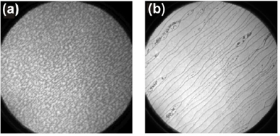
Figure IV.4. Graphene layers grown on the Si-face (a) in vacuum, (b) under Ar [588]. Field of view is 20 µm. The lines are identified as BLG by counting the number of minima in the LEEM reflectivity as a function of the electron beam intensity. Adapted from [588, 589].
Download figure:
Standard image High-resolution imageIV.1.2. Near equilibrium confinement controlled growth
CCS[597] relies on SiC being in near equilibrium conditions with the Si vapour. Graphene growth is controlled by encapsulating the SiC crystals in graphite so as to sequester the evaporated Si (see figure IV.5). A SiC crystal is placed in a closed graphite box (called crucible) provided with a very small calibrated hole of typical diameter 1 mm. As the T of the furnace is increased above 1200 °C and Si sublimates from SiC, the built-up Si vapour remains confined inside the crucible and escapes slowly through the hole (figure IV.5(b)). The SiC chip is therefore in a uniform Si vapour as defined by the PSi versus T of figure IV.2, ensuring uniform graphene growth. Because the Si vapour is confined, the growth T is substantially increased (by ~300 K for CCS [597]) compared to vacuum growth. Details about the full furnace design and operating conditions can be found in Ref. [597, 615]. The Si escape rate that ultimately determines the growth rate, is defined by the geometry of the hole (diameter 0.5 to 2 mm) [597, 615]. The rate of graphene formation by CCS can be reduced by a factor >1000 compared to UHV sublimation, where 1LG grows on the C-face in ~1 min at T = 1.200 °C [597]. The graphene formation rates can be reduced by an additional factor of up to 103 by introducing 1 atm of Ar into the enclosed crucible [597]. The system is compact for fast pumping speed and small thermal inertia, allowing fast heating and cooling rate up 150 °C s−1 in the T range from RT to 2100 °C. The T profile is computer automated [615, 616]. The whole process can be performed in less than two hours, being scalable to full wafer sizes.

Figure IV.5. Confinement controlled sublimation. (a) In UHV Si that is sublimated from the SiC surface at high T escapes. (b) In the CCS method, SiC is in quasi-equilibrium with its own vapour (c) picture of the CCS furnace. Adapted from [597].
Download figure:
Standard image High-resolution imageAn alternative method to CCS is to cover the SiC substrate with a piece of graphite, which provides some Si vapour confinement. The Si escapes on the side providing a non uniform Si vapour gradient that produces narrow tapered stripes of graphene [617].
To grow EG on hexagonal 4H- or 6H-SiC wafers by CCS [615] the key step after pumping out the cell to below 10−6 mbar, is the Si sublimation at high T (1400 °C–1650 °C). The exact T profile depends the geometry of the graphite crucible and geometry of the hole [615], and on the background pressure (with or without additional Ar backpressure). Optimum T and growth times are specific for each crucible adapted to each type of grown graphene. Typically, a 1LG in 20 min at 1520 °C [594] on the Si-face, a graphene buffer layer °C lower than the Si monolayer in the same crucible [594]. On the C-face, N is determined by both T (1450 °C–1525 °C) and time (1 min to several hours for very thick films)[597, 615] [606] (see section IV.1.3 and figures IV.5(a)–(c)). Templated graphene growth of nanostructures (e.g. SiC sidewalls [618–620]) on non-polar facets (i.e. other that (0 0 0 1) and  ) is finely tuned close to the buffer layer growth conditions.
IV.1.3. Carbon-face
The surface state of the substrate prior to growth is essential, because rough surfaces have multiple disordered nano-steps acting as nucleation centres for graphene growth. The first step is therefore SiC surface flattening. For SiC surfaces polished to optical quality, the deep polishing scratches can be removed by SiC etching at high T in a hydrogen environment [621]. Successful flattening is obtained at 1500 °C for 15 min in a flow rate of 200 sccm in 1 atm of a mixture of 5% H2 in Ar [621], which produces a surface with no observable scratches in AFM section IX.1.2 and with a step-terrace structure with atomically flat terraces. However, on the 6H(0 0 0 1) face, the average width and step height of terraces after treatment do not have a clear correlation with hydrogen etching, T and time, but are related to the local miscut angle (the local angle θ of the surface relative to the on-axis orientation, generally θ < 0.2° for commercial wafers of on-axis wafer [621]. Commercial SiC wafers can be purchased with so-called 'epiready surfaces' treated by a chemical mechanical process. These provide excellent starting surfaces, with rms < 0.2–0.3 nm, with no need for etching prior to graphene growth.
On the 4H- or 6H-SiC carbon face, continuous MLG containing 5–10 LG [622] are grown by annealing for 15 min at T in the range 1450 °C–1525 °C. Repeated cycles produce much thicker films up to 50 LG [623, 624]. Shorter times and lower T are required to produce 1LG. They appear in patches on the SiC substrate (see inset of figure IV.7(a)) because of the rapid growth rates on the C-face and the multiple nucleation sites [604, 606, 615, 625].These 1LG have excellent electronic properties, despite draping over steps and making pleats [604].
Sample quality is revealed in AFM (see section IX.1.2) and STM images (see section IX.1.4) in multiple spectroscopy techniques (see section IX)), magneto-optical, photoemission, see (section IX), ultrafast optics and electronic transport (see section IX.3 Raman spectroscopy shows a vanishing D peak attesting the low defect density (see figure IV.7). All spectroscopy studies [622, 624, 627–629] confirm that the MLG behaves as electronically decoupled, i.e. as a stack of graphene layers with a non gapped linear dispersion down to a few meV from the Dirac point, not like graphite and exhibit the quantum Hall effect [604, 625, 630] and high mobility (up to µ = 39 800 cm2 V−1 s−1 at charge density n = 0.19 × 1012 cm−2 [604]). The se MLGare continuous over the entire SiC, drape over SiC steps and have rms < 5 pm as measured by x-ray diffraction [596]. STM shows extended moiré regions [600, 627] providing evidence that adjacently stacked graphene layers are rotated creating a superstructure. On a larger scale, smooth graphene pleats are observed, as seen as bright lines in figures IV.6(c) and (e), which originate from the differential contraction of graphene and SiC upon cooling.
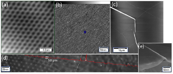
Figure IV.6. MLG on C-face topography images. (a) 4 × 4 nm STM image (reproduced with permission from [626]). (b) 400 × 400 nm STM image. The blue square represents the size of the STM scan in (a) [626]. (c) 40 µm × 40 µm AFM scan. The white lines are graphene pleats. (d) 400 nm long STEM image across areas of different moiré pattern, showing that the top layer is flat (rms < 50 pm) and continuous (from [627], with permission from AAAS). (e) SEM image of a graphene pleat (from [621], with permission from Elsevier).
Download figure:
Standard image High-resolution image
Figure IV.7. Raman spectroscopy for graphene layers on 4H-SiC C-face (a)SLG, inset AFM image. The black trace is the raw data (SiC + Graphene), blue is the bare SiC spectrum; the red trace is the graphene spectrum once the SiC Raman peaks are substracted [631] (b) MLG with the Raman contribution for SiC removed. The inset shows a Lorenzian 2D peak for this 10LG. Figure adapted from [630], © IOP Publishing.
Download figure:
Standard image High-resolution imageMLGs have been used as a model system to study graphene properties [585]. This stems from a combination of factors: (i) Excellent structural quality (small Raman D peak observed, see figure IV.7 and [630]), (ii) Flatness of the layers (rms < 5 pm as measured by x-ray diffraction [596]) which excludes strain-related gauge field effects [632] and broadening effects in k-resolved spectroscopy measurements (see figure S1 in supp of [620]), (iii) Small interaction with the substrate and the environment, particularly for the layers in the middle of the stack that are quasi-neutral [629, 633] (charge density n ~ 5 × 109 cm−2, that is at most 8 meV away from the Dirac point) with high mobilities at RT [628, 633]. (iv) graphene electronic structure for all layers [634], due to the rotational stacking, providing a large signal intensity very much sought in optical measurements.
IV.1.4. Silicon-face
MLG on Si-face (see figure IV.4) is the most studied as for realization of quantum resistance standards (as multiples of h/e2 = 25.812 807 kΩ) at 4.2 K in small (<1 Tesla) magnetic fields. With a quantum Hall resistance quantization accuracy of 3 × 10⁻⁹ that rivals the best 2d electron gas standards [612, 635]. As growth on the Si-face starts from the SiC steps [601, 603, 636], BLG (or MLG) tend to form at step edges when a 1LG fully covers the terrace (see figure IV.4), which makes it difficult to produce extended 1LG. Additionally, the step edges add electronic scattering due to the presence of BLG/MLGH, or to the reduction of the carrier concentration on the step [585], which is detrimental to the homogeneity of the quantum Hall effect [637]. Better control of growth on the Si-face was obtained by providing carefully balanced methane and H2 [638]. Ref. [639] reported MEG draped continuously over the steps by graphitization of a polymer deposited on the bare SiC.
IV.1.5. Step bunching and graphene growth
During annealing above 1200 °C, the SiC surface undergoes microscopic restructuring by forming steps and terraces. This process, known as step bunching [1745], is different from atomic surface reconstruction and refers to surface morphology. Step bunching, i e. the bunching of straight steps on vicinal crystal surfaces, which is governed by energy minimization on different terraces is a fundamental phenomenon in SiC. Graphene formation has been analyzed with respect to step bunching of SiC, by studying the influence of the crystal structure at the atomic level for each SiC polytype [640]. As illustrated in figure IV.8(a), the 4H-SiC polytype has two decomposition energies, terraces 4H1 (−2.34 meV) and 4H2 (6.56 meV), respectively, and the 6H-SiC (figure IV.8(b)) has three distinct terraces, 6H1 (−1.33 meV), 6H2 (6.56 meV) and 6H3 (2.34 meV), while 3C-SiC (figure IV.8(c)) has only one kind of terrace, 3C1 (−1.33 meV) [640].
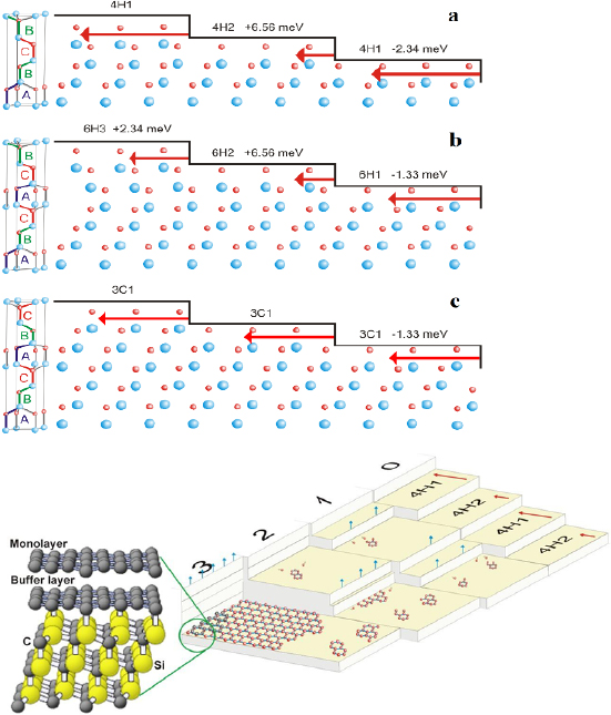
Figure IV.8. Stacking sequences and possible terraces on (a) 4H-SiC, (b) 6H-SiC, and (c) 3C-SiC surfaces. Large (blue) and small (red) circles represent Si and C atoms, respectively. Length of arrows indicates different step decomposition velocities. (d) Schematic depiction of the formation process of EG via sublimation of Si from the SiC surface. Adapted from [640], with permission from Elsevier.
Download figure:
Standard image High-resolution imageThe growth process is schematically shown for 4H-SiC in figure IV.8(d). Since Si and C atoms are bonded more weakly in the vicinity of step edges, Si desorbs from these areas faster in comparison with the terraces [601, 603, 636]. Based on the terrace energies, removing a 4H1 terrace costs less energy and the step decomposition velocity is faster (figure IV.8(a)). As shown in figure IV.8(d), from the edge of the 4H1 terrace on the graphene-free surface, C atoms are released onto the terrace as Si atoms leave the surface (stage 1). The C atoms coalesce and nucleate into graphene islands (stages 1 and 2), which act as a sink for subsequently released C atoms. After the 4H1 terrace step catches the 4H2 step, the newly formed two SiC bilayer step provides more C atoms as compared to the one-bilayer step and the first graphene layer extends along the step edge (stage 2). The large percentage of bunched steps with four Si-C bilayers, an increased source of C, will impose the formation of a second layer of graphene (figure IV.8(d), stage 3) since some extra C will be released. Therefore, a full coverage of the 4H-SiC substrate surface by just 1LG may be an issue.
A similar mechanism of energy minimization is expected in the 6H-SiC polytype (figure IV.8(b)). As a result, first the step 6H1 will catch step 6H2 and forms two Si-C bilayers. Then step 6H3 will advance and merge with the two-bilayer step. The growth process for 6H-SiC is the same as the 4H-SiC [640]. However, on 3C-SiC all terraces have the same decomposition energy [640] (figure IV.8(c)) and no energetically driven step bunching should be expected. In this polytype, a non-uniformity of sublimation may be induced by the presence of extended defects such as stacking faults, which are characteristic of this material [641].
A capping technique can be employed to localize the step bunching [642]. The cap consists of an amorphous carbon layer evaporated on the bare SiC grid evaporated on the bare SiC. Amorphous carbon is then patterned by plasma etching or lift-off to produce typically micron size structures. Upon annealing to produce graphene, the carbon layer pattern pins the SiC steps under it so that the SiC steps bunch against one enclosure wall and align along the amorphous C grid, as shown in figure IV.9(a). Several geometries have proven effective, and it is reasonable to position an edge of the cap perpendicular to the SiC substrate miscut to maximize step bunching against the cap wall. The slight SiC surface roughness induced by the mild plasma etch used to pattern the carbon layer (see figure IV.9(c) top) is smoothed out by the step bunching at the high T of the graphene growth (see figure IV.9(c) bottom). This technique provides large flat terraces (figure IV.9(c)-bottom) at a predefined location. The amorphous C is finally removable by plasma etching after annealing to access the graphene layer for further device patterning [642]. In that case a graphene protection layer is used (this can be the dielectric of a subsequent top grid).
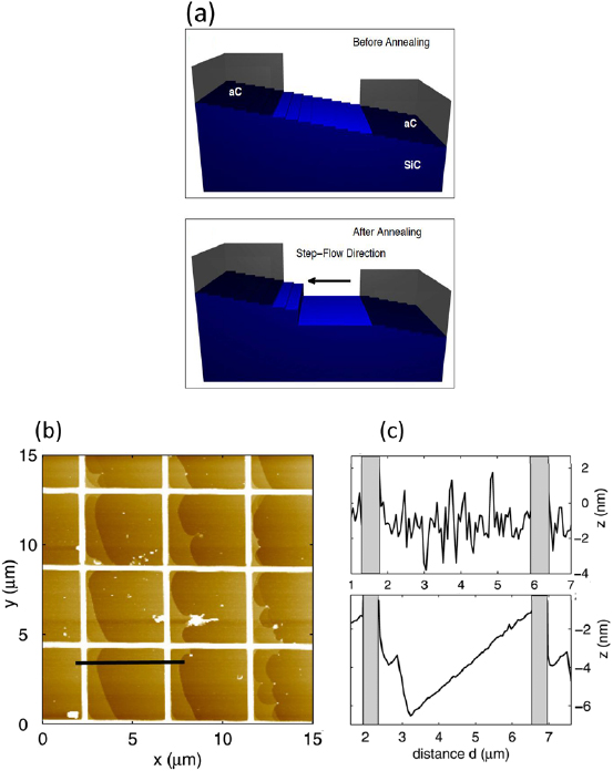
Figure IV.9. SiC Step pinning under an evaporated amorphous carbon grid. (a) Schematics of step pinning (before annealing, upper frame). After annealingat 1350 °C (lower frame), the steps accumulate at one side of the grid in each enclosure providing large terraces at a locations defined by the grid. The arrow point the direction of the flow. (b) AFM image after annealing and (c) topographic profile within the grid (top) before and (bottom) after step bunching annealing, showing that a large terrace has developed. Adapted from [642], with the permission of AIP Publishing.
Download figure:
Standard image High-resolution imageIV.1.6. Optimization of growth process for scale up
Growth conditions can be developed to increase the size of the SiC substrate to 20 × 20 mm2 and ultimately to 100 mm diameter wafers. The furnace is similar to that of figure IV.3, but with longer RF-coil with uniform distance between the pipes [643]. The coil can be moved up and down to change the T gradient if necessary and it is fully automatic. The key to achieve large area 1LG on SiC is to (a) understand the role of the buffer layer [590, 592, 610] and of the step bunching [607] which takes place during its formation and to monitor the effect of (b) T (in the range 1700 °C–1950 °C); (c) Ar pressure (in the range 750–950 mbar) (d) and growth time (from 0 to 15 min). AFM topography and phase images show that the formation of the buffer layer (at 1850 °C and Ar pressure 950 mbar) can start at any place on the substrate, but preferably on the kink of steps, as shown in figure IV.10(a). The C atoms coalesce and nucleate into graphene islands on the step kinks (marked with a circle) and these islands act as a sink for other C atoms. As the step edges are the main source of C, the growth rate is two times higher along the step edge compared to that on terraces and for this reason a graphene layer first covers like a ribbon the sidewall of steps (figure IV.10(a)) [602, 618, 620, 644].Then growth continues from the edge of a step to the (0 0 0 1) terraces, where the graphene layer interacts with the surface and becomes the buffer layer. Studies show that the graphene layer first covers the steps with larger terrace [643]. A critical issue is to fully cover the substrate surface by a buffer layer, before lifting it up as a 1LG by growing another buffer under it. A good quality buffer layer exhibits a particular pattern in LEED, as illustrated in figure IV.10(b) (see also figure IV.10(b), and [584, 592, 611, 645–647]. The pattern for a buffer layer grown in the reactor of figure IV.3 at 1850 °C and 850 mbar is similar over the whole surface.

Figure IV.10. (a) AFM phase images of initial stage of the buffer layer formation, and (b) LEED pattern of the buffer layer (electron energy 60 eV) grown under Ar (in the reactor of figure IV.3) [643].
Download figure:
Standard image High-resolution imageSimilarly to the amorphous C corral [642], the buffer layer can stop the step bunching process on 4H and 6H-SiC [648]. This means that the surface energy becomes uniform all over the substrate surface after the formation of the buffer layer subsequently resulting in a uniform and continuous 1LG coverage, which does not exclude the growth of BLG at the steps. The T dependence of the buffer layer formation and SLG coverage is sublinear (that is close to linear, not exponential [643]), which suggests that the synthesis is surface kinetics limited on both SiC polytypes [601, 643]. The results from graphene samples grown Ar indicate that there is an optimal Ar pressure (~850 mbar) yielding under this condition a high growth rate.
The time dependence of SLG and BLG growth under Ar pressure shows that graphene spreads faster on 4H-SiC substrates than on the 6H polytype from the start of the growth, and that 1LG coverage increases approximately linearly with time. After the SLG is complete, increasing annealing time does not significantly increase the BLG coverage for both 4H and 6H-SiC polytypes [643].
Based on the above results, a growth protocol was defined to optimized SLG coverage. The result, shown in figure IV.11 indicate the growth of ~99% 1LG on 20 × 20 mm2 SiC substrates and 99.8% 1LG for 7 × 7 mm2 substrate (figure IV.11). The SLG coverage is determined by optical reflectance maps. Experiments showed that the reflectance of graphene on SiC normalized to the reflectivity of bare substrate (the contrast) increases linearly ~1.7% per layer for up to 12L, which agrees with theory [649]. The wavelength dependence of the contrast in the visible is investigated using the concept of ideal Fermions and compared with existing experimental data for the optical constants of SLG [649].
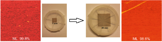
Figure IV.11. Size increase of 1LG from 7 × 7 mm2 to 20 × 20 mm2. The size of reflectance maps (red scale) are 30 µm × 30 µm [643].
Download figure:
Standard image High-resolution imageThe results for SLG on 4-inch SiC wafer showed that the growth rate on the edge of the wafer is higher than in the centre, due a faster Si escape at the wafer edges [597]. Quasi-equilibrium growth [597] provides a way to mitigate these problems. Figure IV.12 shows the recipe for growth of SLG on large area substrates, including on 4 inch SiC wafer. These operation conditions assume different T ramps up to 1150 °C and to the growth T, according to figure IV.12.
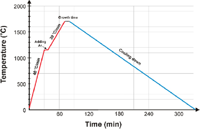
Figure IV.12. Temperature-time plot for the growth of SLG on 4 inch substrates under Ar [643].
Download figure:
Standard image High-resolution imageIV.1.7. Growth on SiC off-axis cut surfaces
Graphene layers are best grown on 4° and 8° off-axis 4H-SiC (0 0 0 1) substrates to have the right terrace width for performing step flow growth [650, 651]. A general recipe is provided in Ref. [652]. Figure IV.13 shows a side view of the off-axis SiC substrate used for graphene growth, where the off-axis surface is tilted at a specified angle (off-axis angle) from the basal plane surface toward the  ] SiC direction. Controlling the tilt angle allows to change step heights, terrace widths and a growth rates.

Figure IV.13. (Top panel) Diagram illustrating off-axis surfaces of 4H-SiC and (bottom panel) schematic drawing of the off-axis 4H-SiC surface after graphitization [643].
Download figure:
Standard image High-resolution imageA direct comparison of graphene formation on an 8°-off axis (0 0 0 1) 4H-SiC epitaxial layer and on-axis (0 0 0 1) 6H-SiC [653], performed by uniform graphitization of 1 cm × 1 cm SiC substrates at 2000 °C for 30 min (with a base pressure in the chamber ~5 × 10⁻⁶ mbar and an argon pressure ~1 atm during the growth) shows that the growth of graphene on off-axis SiC starts from the edge and follows the surface of the large terraces (0.5 to 1 µm width), running parallel to the original steps of the off-axis wafer.
Off-axis samples present significant step bunching after high T annealing (rms = 16 nm), while flatter surfaces (rms = 2.4 nm) are obtained on the on-axis sample. In comparison with on axis SiC wafers, off-axis SiC wafers contain a lot of steps due to their cuting angle. For this reaseon, during annealing they easily bunch. Step bunching is higher in off-axis samples with dense step edge, because etching or erosion start from on step edges, which is not the case in on-axis samples. A more uniform and homogeneous graphene coverage was found on on-axis 6H-SiC [653]. The 100 to 200 nm wide terraces of the 4H-SiC (0 0 0 1) 8° off-axis samples are covered by FLG spreading like a carpet for all growth T in the range 1600 °C to 2000 °C (growth under Ar) [654], with an increase in the N as a function of T (from 0 to 10 LG) (figure IV.14).
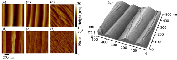
Figure IV.14. (Left panel) AFM images. Effect of graphitization temperature on the surface morphology of the sample 8°-off axis (0 0 0 1) 4H-SiC: 1600 °C (a), 1700 °C (b) and 2000 °C (c). The phase contrast maps on the same samples are also demonstrated ((d)–(f), respectively). (right panel) STM image of a sample annealed at 2000 °C. Adapted from [654], with permission of The Royal Society of Chemistry.
Download figure:
Standard image High-resolution imageSimilarly to the on –axis surface, the graphitization rate is much higher for the C-face off axis substrates while it is almost an order of magnitude smaller for the Si-face on-axis substrate compared to off axis substrates (figure IV.15). AFM analysis showed the presence of the steps with different heights. An ~0.35 nm and ~1.1 nm step height can be associated to 1 and 3LG, respectively, over the substrate or stacked over other graphene layers [601]. In fact, like for the (0 0 0 1) on-axis face, the graphitization starts from the step edges and propagates gradually to the centre of the terrace [601–603, 655]. In this case, the C atoms at terrace kinks and step edges have a lower coordination number, thereby leading to an easier breaking of the bonds at these sites. For this reason, the probability of SiC decomposition and further surface diffusion of C atoms is increased and graphitization of the SiC surface occurs [655]. Regarding the growth kinetics, anisotropy of the Si desorption rate is always present and, thus, different SiC steps have different evaporation rates [601]. In addition, increase in the miscut angle increases the step density, thereby leading to an increase in graphene thickness at this region [601].
Figure IV.15. Graphitization thickness versus T at 60 min for 8° off cut Si- and C-face 4H SiC and for Si-face on axis 4H substrate (adapted with permission from [614]).
Download figure:
Standard image High-resolution imageAnother interesting finding (see figure IV.14—right) is that the presence of the atomic steps leads to the formation of pleats similar to the MEG on the 4H/6H on-axis C- face (~1 to 2 nm high and 10 to 20 nm wide) preferentially oriented in the direction perpendicular to the step edges of the SiC terraces (figures IV.14(e) and (f)) [654]. Such a parallel orientation of pleats is particular to SLG grown on a vicinal SiC surface, while for SLG grown on on-axis 4H-SiC it is characterized by a preferentially hexagonal mesh-like network of pleats interconnected into (often) triangular nodes [585] (see figure IV.14(c)).
IV.1.8. Growth on non-polar surfaces SiC
The presence of the buffer layer on the Si-face is often argued to degrade the electronic properties of the SLG above it [656–659]. In quasi -free standing SLG the buffer layer is converted into SLG by intercalation. An alternative to intercalation is the direct graphitization of non-polar SiC surfaces where there is no buffer layer [660, 661], or to master the graphitization on 1LG on the C-face, where high mobilities are measured [604].
According to the crystallography of the hexagonal family of SiC, there are three non-polar planes available for graphene formation: the m-plane  , a-plane
  and r-plane
  [661]. Figures IV.16(a) and (b) show the possible polar and non-polar SiC planes for graphene growth. In addition, the growth of graphene can be performed using thermal decomposition of (0 0 1)-oriented cubic SiC [661]. However, the commercial production of 3C-SiC substrates is limited, and in contrast to 4H and 6H-SiC, large single crystals 3C-SiC are not available. Polycrystalline 3C-SiC are often grown as epilayers on SiC or on Si-wafers. Figures IV.16(c) and (d) demonstrates the important crystallographic planes in the cubic structure of SiC.

Figure IV.16. Principal crystallographic planes of (a,b)hexagonal and (c,d) cubic SiC.
Download figure:
Standard image High-resolution imageSynthesis of graphene on on-axis (0 0 1) cubic SiC substrates can be performed at T >1800 °C for 20 min in a C rich atmosphere [661]. To provide reliable control of graphene formation a low growth rate (~1LG per five minutes) should be maintained, which is realized in a close crucible at a Ar gas pressure of 800 mbar.
Optimization of parameters (e.g., lowering T from 2000 °C to 1800 °C) can be effective for obtaining graphene layers with desired thicknesses and domain sizes ~100 nm. The optimizacion of the rest of parameters, like pressure, flow rate, step bunching, time, etc follow the same trend that for samples grown on non-polar faces and that are described in previous paragraphs. Figure IV.17 shows the LEEM images of graphene before and after optimization i.e at T = 1800 °C in the reactor of figure IV.3.
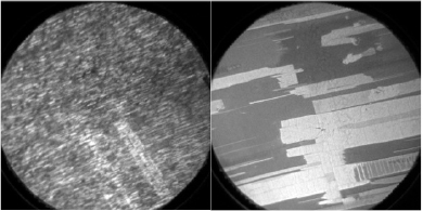
Figure IV.17. LEEM images of graphene grown on (0 0 1) cubic SiC before (left panel) and after optimization (right panel). In the first case, we have 4–5LG, while optimized growth allows to obtain 1–3 LG with increased domain size up to 10 µm. Field of view is 25 µm. Adapted from [661].
Download figure:
Standard image High-resolution imageA (0 0 1) cubic SiC substrates with rather flat surface and low surface roughness (rms~2 nm) obtained by substrate polishing (rms ~0.6 nm) promotes growth of more homogeneous EG with large domain sizes as shown in figure IV.17. Growth on  6H-SiC resulted in non uniform coverage exhibiting areas of fragmented graphene and some micrometre large areas (figure IV.18—left). Similar results were reported in Ref. [662] for the
  plane (figure IV.18—right).
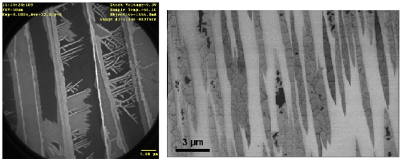
Figure IV.18. (left) LEEM image of graphene grown by thermal decomposition at 1900 °C on  oriented 6H-SiC substrates, scale bar 5 micron, adapted from [643]. (right) SEM image of graphene grown on 6H-SiC, scale bar 3 micron
  .
.
Download figure:
Standard image High-resolution imageGrowth on non-polar SiC surfaces is limited by the vertical growth rate (graphene growth on the polar face proceeds laterally) [641]. Such vertical growth produces scattered islands of graphene on the surface with higher density of grain boundaries (see figure IV.19). The latter causes a greater amount of Si out-diffusion from the substrate, leading to a thicker (up to 8LG) subsequent [607] MLG growth on the nonpolar faces in comparison to growth on polar faces [607]. As graphene growth on the low-packed non-polar planes is faster than that on the high densely packed non-polar planes, it is assumed that the surface density is a key factor limiting Si desorption and the graphene growth rate.
Figure IV.19. Graphene growth mechanism on (a) the polar (Si) face SiC with offcut toward [ ] and (b) the nonpolar a/m face with slight offcut along [0 0 0 1]. The growth on the polar face proceeds laterally while the growth on the nonpolar face is limited by the vertical growth rate. The zigzag structure shown on the polar face step edge is a consequence of two possible lateral growth directions. Adapted from [667], copyright American Chemical Society.
Download figure:
Standard image High-resolution imageIV.1.9. Surface engineering by intercalation
Graphene grown on SiC(0 0 0 1), by sublimation resides on top of a buffer layer [590, 592], as schematically depicted in figure IV.20. The buffer layer (denoted also by 6 √ 3) is formed at the early stages of heating of the samples, i.e. before graphene is formed, and it has been observed in several experimental studies of of SiC(0 0 0 1) surfaces [586, 663–665] and also in an atomistic simulation of graphene formation on SiC(0 0 0 1) [590, 666]. The buffer layer has a (6 √ 3 × 6 √ 3)R30° periodicity with respect to SiC(0 0 0 1) substrate surface.
Figure IV.20. Schematic view of graphene on SiC(0 0 0 1). The graphene layer resides on top of the buffer layer. The buffer layer is structurally equivalent to graphene but strongly bound to the SiC substrate. Dangling bonds (db) are present due to the lattice mismatch between graphene and SiC. Drawing not to scale (after [645, 670]).
Download figure:
Standard image High-resolution imageThis layer consists of C atoms in a graphene arrangement [590, 592, 668]. This means that the structure is has C hexagons with a C–C distance like in graphene. The (6 √ 3 × 6 √ 3)R30° periodicity with respect to the SiC surface corresponds to a (13 × 13) super cell. Thus, the super cell contains 169 graphene unit cells. Due to a hybridization of states of the C atoms of the buffer layer with states from the SiC substrate surface, it lacks the typical π-bands of graphene and therefore has no Dirac cone [592]. On the other hand, the σ-bands of the buffer layer are fully developed and indistinguishable from those of graphene [592]. These observations are in agreement with theoretical studies [590, 669].
The buffer layer (6 √ 3) induces electron doping in SLG. Typical values for the charge carrier density in SLG are n ~ 1 × 1013 cm−2 [589, 671–674]. The buffer layer is also partly responsible for the relatively low µ and its T dependence [658]. Furthermore, the reduction in spin transport in SLG is attributed to the buffer layer [656]. Typical values for µ ~ 1000 cm2 V−1 s−1 at n ~ 1 × 1013 cm−2 and T = 300 K and µ ~ 2000 cm2 V−1 s−1 at n ~ 1 × 1013 cm−2 and T = 25 K [584, 589, 658, 675, 676].
The structural similarities between the buffer layer and graphene suggest that it should be possible to convert the former one into the latter by cutting the bonds between buffer layer and substrate through intercalation, as depicted in figure IV.21 schematically for the case of hydrogen. Similar procedures have been studied before for SLG on metal surfaces like, e.g. Ni(1 1 1) [677]. In this case, different metals like Au, Yb, or Cu were intercalated between the metal substrate and graphene [677]. Several authors showed that different elements can be intercalated between the buffer layer and the SiC substrate. E.g., the intercalation of H [645–647, 658, 678–681], O [682–685], F [686, 687], N [688], Si [689, 690], Ge [691, 692], Au [693–696], Cu[697], Li [698, 699], Na [700] and subsequent transformation of the buffer layer into graphene have been confirmed.
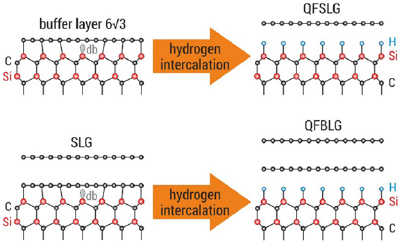
Figure IV.21. Schematic view of the conversion of the buffer layer into quasi-freestanding SLG on H-saturated SiC(0 0 0 1) (also referred to as SiC(0 0 0 1)-H) and of SLG on the buffer layer into quasi-freestanding BLG on SiC(0 0 0 1)-H. After [645, 670].
Download figure:
Standard image High-resolution imageFor applications, it is important that the intercalated species does not give rise to electronic states at the Fermi level, since these would short-circuit the graphene layer on top of it. This is the case for hydrogen which saturates the SiC(0 0 0 1) surface with Si–H entities.
The doubly filled bonding and empty anti-bonding Si–H states are located below and above the valence band minimum and valence band maximum, respectively, leaving the surface electronically passivated [701–703]. A similar situation can be expected for oxygen and fluorine passivation of the SiC(0 0 0 1) surface.
The first study of the intercalation of hydrogen under the buffer layer on SiC(0 0 0 1) was reported in Refs. [645, 646] who annealed SiC(0 0 0 1) substrates covered by the buffer layer in one atmosphere of hydrogen at T between 600 °C and 1000 °C. Similar processes can be employed to intercalate hydrogen under the buffer layer even if an additional graphene layer already exists on top of it [645, 646, 657, 680, 704–706], although the exact conditions may vary. In this case, SLG becomes a quasi-freestanding BLG (see figure IV.21).
The successful decoupling of the buffer layer and conversion into so-called quasi-freestanding SLG was confirmed by LEED, ARPES, XPS and LEEM. Figure IV.22(a) shows typical XPS spectra of the C1s core level of various samples [707]. The spectrum of the buffer layer is has 3 components. S1 and S2 are caused by the C atoms of the buffer layer [592]. In addition, a component due to C atoms in the SiC substrate is visible. These are also seen in the spectra of SLG, BLG and TLG indicating that the buffer layer forms the interface. Upon H-intercalation, the buffer layer is converted to SLG which is evident from the disappearance of the components S1 and S2 and the formation of a graphene-related component. This is also the case for SLG/BLG. The component of the SiC substrate is shifted to lower binding energy due to a change of surface band bending. Figure IV.22(a) shows examples of the band structure near the K-point of the hexagonal Brillouin zone as measured by ARPES [707] for SLG, BLG.
Figure IV.22. (a) C1s core level spectra of the buffer layer, SLG, BLG, =TLG and TLG, on substrated and quasi freestanding (QF). The H-intercalation leads to a disappearance of the buffer layer components (S1, S2) and an increase of the graphene-related component. The signal due to SiC shifts to lower binding energy due to a change of band bending. (b) ARPES intensity maps versus electron energy and momentum of SLG and BLG on the buffer layer as well as QFSLG and QFBLG on H-terminated 6H-SiC(0 0 0 1). (c) Si–H stretch mode of the H-saturated SiC(0 0 0 1) surface below QFSLG and QFBLG. (d) Representative Raman spectra of QDSLG and QFBLG. (a) adapted from [708] and (b) adapted from [707], both © IOP Publishing Ltd; (c) and (d) adapted with permission from [704].
Download figure:
Standard image High-resolution imageThe charge carrier type is changed from electrons in SLG/BLG on the buffer layer to holes in QFSLG/QFBLG on the H-terminated (0 0 0 1) surface of hexagonal SiC polytypes [645, 646, 658, 704, 707, 708]. This is due to the spontaneous polarization of hexagonal SiC [708, 709], which varies with the polytype due to their different ratio of hexagonal to cubic stacking sequences [708–710]. For semi-insulating 6H- and 4H-SiC(0 0 0 1)-H substrates hole densities of 6.2 × 1012 cm−2 and 8.6 × 1012 cm−2, respectively, as determined by ARPES in good agreement with theoretical predictions [708–710]. In the case of QFSLG on n-type doped cubic 3C-SiC(1 1 1)-H a slight electron doping is observed, which agrees with the fact that this SiC polytype has no spontaneous polarization. In this case the excess electrons in QFSLG is due to alignment of the Fermi levels as described by the Schottky model for metal–semiconductor interfaces [708]. Refs. [658, 704] have provided evidence for the hydrogen at the interface by measuring the Si–H stretch mode vibration using FTIR absorption spectroscopy as shown in figure IV.22(c). This was later confirmed by surface enhanced Raman spectroscopy [711, 712]. Raman spectroscopy also provided evidence for the conversion of the buffer layer to a QFSLG [658, 705, 711, 712]. In the case of QFSLG a narrow 2D line is observed while for QFBLG a broad 2D line indicative for AB stacking is found (see figure IV.22(d)). Electronic transport studies on simple Hall bar structures and FET have shown that QFSLG on 4H- of 6H-SiC(0 0 0 1)-H exhibits a higher charge carrier mobility (typically ~4000 cm2 V−1 s−1) than SLG on the buffer layer and that it has a considerably reduced T dependence [658, 704, 705, 713–718].
Decoupling of the buffer layer from the SiC substrate and saturation of the SiC(0 0 0 1) surface with hydrogen can be carried out in an apparatus depicted in figure IV.23 [719], initially designed for the hydrogenation of SiC surfaces [703, 719, 720]. The system consists of a quartz tube in which the sample can be heated in an atmosphere of purified hydrogen in a contact-less manner by means of halogen lamps. In the hydrogenation process, the chamber is first filled with hydrogen and then the sample is raised to the desired value. Typical process parameters are listed in table IV.1.

Figure IV.23. Sketch of the apparatus used for intercalating hydrogen between the buffer layer and the SiC(0 0 0 1) substrate [658, 704, 708]. After [719].
Download figure:
Standard image High-resolution imageTable IV.1. Typical parameters for intercalating hydrogen under the buffer layer [658, 704, 708].
| Process | Sample temperature in °C | Hydrogen pressure in mbar | Flow rate in slm | Time |
|---|---|---|---|---|
| 6 √ 3 to QFSLG | 540–560 | 900–960 | 0.9–1.0 | 60–90 |
| SLG to QFBLG | 840 | 900–960 | 0.9–1.0 | 60–90 |
Variations of the above procedure have been reported for the synthesis of quasi-freestanding graphene layers on SiC(0 0 0 1). Ref. [645], reported preparation T in the range from 600 to 1000 °C at atmospheric pressure without mentioning the annealing time. Ref. [713] annealed in molecular hydrogen to convert SLG to QFBLG. They reported a H2 pressure of 800 mbar, T of 600 to 1200 °C, and process times between 30 and 120 min. Ref. [721] carried out the hydrogen annealing directly after the growth of graphene in a Hot-Wall CVD reactor. After graphene growth in Ar at 100 mbar at 1650 °C, the sample was cooled to 1050 °C. At this T, the gas a exchanged to H2 and the pressure increased to 900 mbar. After 30 min, the sample was allowed to cool to 700 °C in H2. Finally the system was evacuated and the sample allowed to cool to RT. Ref. [715] annealed their buffer layer samples in H2 at 1013 mbar and temperatures between 600 and 1200 °C for 60 min. In Ref. [706], QFSLG was produced by annealing in a furnace at 800 °C and a H2 flow of 0.2 slm for 1 h at an unspecified pressure. The process time was 60 min. The highest mobility was observed for at of 700 °C. In [706] QFBLG by annealing Hall-bars made from SLG at 1250 °C in H2 at ~33 mbar was reported. Ref. [680] employed a plasma source as well as an atomic hydrogen source to convert SLG to QFBLG. They reported that the plasma treatment induces a disorder. Kinetic Monte Carlo simulations performed in Ref. [722] have shed light on the atomistic mechanism of H intercalation of the buffer layer, in good agreement with experiments.
Surface analytical tools such as LEED, XPS(see section IX.2/XPS for an introduction to the technique), ARPES (see section IX.2.3 for an introduction to the technique), LEEM and STM (see section IX.1.4 for an introduction to the technique) along with FTIR and Raman are ideally suited to characterize the quasi-freestanding graphene layers on H-terminated SiC(0 0 0 1). Table IV.2 lists several methods together with the expected observation and relevant references.
Table IV.2. Characterization techniques for QFSLG and QFSLGon H-terminated SiC(0 0 0 1).
| Method | Observation | References |
|---|---|---|
| Process: buffer layer 6 √ 3 to QFSLG | ||
| LEED | Strong weakening of the superlattice diffraction spots caused by the buffer layer | [645–647] |
| XPS | Disappearance of the C1s signals related to the buffer layer and appearance of an asymmetric C1s signal due to QFSLG; Shift of the C1s signal related to the SiC bulk to lower binding energy due to a change of surface band bending (see figure IV.22(a)) | [647, 704, 708] |
| XPS | Shift of the C1s signal related to the SiC bulk to lower binding energy | [647, 704, 708] |
| ARPES | Appearance of a graphene π-band at the K-point of the hex. Brillouin zone with the Dirac point located above the Fermi level (see figure IV.22(b)) | [645–647, 703, 708] |
| LEEM | Transition from a flat LEEM-I(V) curve to a spectrum with one dip | [647] |
| STM | Topography image without buffer layer moiré structure | [668, 707, 715] |
| FTIR | Appearance of a sharp Si–H stretch mode signal (see figure IV.22(c)) | [658, 704] |
| Raman | Disappearance of the broad Raman spectrum of the buffer layer and appearance of sharp G and 2D bands; 2D band symmetric (see figure IV.22(d)); | [658, 704, 713, 717, 724, 725] |
| Process: SLG to QFBLG | ||
| XPS | Disappearance of the C1s signals related to the buffer layer and increase of the asymmetric C1s signal due to QFSLG(see figure IV.22(a)) | [645, 680, 704, 708, 713, 721] |
| XPS | Shift of the C1s signal related to the SiC bulk to lower binding energy (see figure IV.22(a)) | [645, 680, 704, 708] |
| ARPES | Disappearance of the linear π-band of graphene with the Dirac point below the Fermi level and appearance of the two parabolic π-bands of BLG with the Dirac point located above the Fermi level (see figure IV.22(b)) | [645, 704, 708] |
| LEEM | Transition from a LEEM-I(V) curve with one dip to a spectrum with two dips | [645, 646, 680] |
| STM | Topography image without buffer layer Moiré structure | [707] |
| FTIR | Appearance of a sharp Si–H stretch mode signal (see figure IV.22(c)) | [704] |
| Raman | Disappearance of the broad Raman spectrum of the buffer layer and change of the symmetric 2D band to an asymmetric 2D band considerably broader than that of QFSLG | [704, 713] |
Oxygen intercalation was suggested a means for decoupling the buffer layer from the SiC(0 0 0 1) surface by annealing the buffer layer [682] in one atmosphere of molecular oxygen at 250 °C for 5 s, using a special oxidation chamber. In the first approach in Ref. [685] the buffer layer samples was annealed in situ, i.e. directly in the UHV chamber used for XPS and ARPES analysis, at 750 °C in ~10−4 mbar of molecular oxygen. The second procedure in Ref. [685] was carried out ex-situ by annealing in O2 with best results at 270 °C at 200 mbar. The Raman spectra, however, demonstrated that both processes lead to the formation on numerous defects. In Ref. [683] the oxygen intercalation to transform SLG into a BLG was carried out by annealing in air at 600 °C for 40 min. A heat up ramp of 50° per minute was used. They confirmed the decoupling of the buffer layer and the formation of a high quality BLG.
In Ref. [684] buffer layer samples as well as SLG were annealed up to 500 °C and 650 °C, respectively, in a water vapour in order to decouple the buffer layer by oxidation of the SiC(0 0 0 1) substrate surface. Raman spectroscopy indicated numerous defects. However, like as for Ref. [683], the QFBLG formed by treating SLG showed a negligible D band. This was also evident from Hall effect measurements, which indicated µ ~ 790 cm2 V−1 s−1 at a rather high hole concentration of 2 × 1013 cm−2. While oxidation of the SiC interface by oxygen or water intercalation leads to highly defective QFSLG, this technique is promising for the synthesis of decoupled QFBLG on SiC(0 0 0 1). One may speculate that the buffer layer, which is highly corrugated and in which C atoms are partially sp3 hybridized [723], is more prone to be attacked by the oxygen during intercalation. On the other hand, in the case of SLG, the buffer layer is protected by the graphene layer on top of it.
Intercalation with other elements was also studied. Contrary to Si, that intercalates only at T > 800 °C through migration at graphene domain boundaries and other defects, Li [698, 699] was found to penetrate into the C layer already at RT through the formation of Li-compounds. Na partial and inhomogeneous intercalation occurs already at RT directly after deposition, although most of the Na remained on the surface and formed Na droplets. Na intercalation is promoted both by electron/photon beam exposure and by moderate annealing at ~100 °C. Annealing at higher T results in de-intercalation and Na desorption from the surface [700]. Other elements intercalation would be appealing, such as nitrogen, that is predicted to provide charge neutral QFSLG [726]
Finally, we review studies on Ge [691, 692] and Au [693–696] intercalation between buffer layer and SiC(0 0 0 1) surface. In both cases, the preparation is performed using the following scheme. First, a thin layer (up to 5 monolayers) of the intercalant (Ge or Au) is deposited on the buffer layer using thermal evaporation. Then, the sample is annealed in UHV to induce intercalation. The properties of the QFSLG formed by intercalation depend on the amount of material present at the interface. For Au two phases were observed [693]: a highly n-type doped one with the Dirac point located ~0.9 eV below the EF for 1 monolayer Au at the interface and a weakly p-type doped phase with the Dirac point at 0.1 eV above EF for one third of a monolayer Au at the interface. Spin-resolved ARPES indicated a Rhasba-type spin–orbit coupling in the π-band of QFSLG at energies where it interacts with Au bands [696]. In the case of Ge [691], an n-type doped QFSLG is obtained when 1 monolayer of Ge resides at the interface while a p-type doped QFSLG is observed when 2 monolayers of Ge are intercalated. The hole and electron concentrations in the QFSLG were ~p = 4.1 × 1012 cm−2 and n = 4.8 × 1012 cm−2. This means that the shift of the Dirac point with respect to EF is almost symmetric. Note that a mixed phase can also be prepared in which n- and p-type regions coexist.
This was employed by Baringhaus et al [692] to fabricate pn-, np-, pnp- and npn-junctions which were investigated by 4-point probe transport measurements. Evidence for Klein tunnelling of charge carries across such barriers was observed.
IV.1.10. Structured growth
The fact that growth starts at a step edges on the SiC(0 0 0 1) face (see above), can be used to produce graphene nanostructures for electronics. Masking methods, for selective growth using AlN [727], SiN [728] and amorphous C masks [642] with tens of nm precision have been proposed. The template growth method on sidewalls of SiC trenches [604, 615, 618, 619] is described below. It circumvents the detrimental effect of traditional plasma etching [729, 730] and resulting sidewall nanoribbons show RT ballistic transport properties [620].
The idea is to tune the parameters so to stop growth just as graphene covers the step sidewalls. Steps can be either natural steps obtained by step bunching at the SiC surface, or the sidewall of trenches of various shape etched in the SiC substrate. The width of the ribbon is then set by the step height and the angle with the basal (0 0 0 1) plane (~27°). Upon heating in the 1400 °C–1600 °C range for graphitization, the SiC steps flow to produce the equilibrium facets at that T. E.g., for ribbons oriented along the graphene armchair direction, stable facets are found at  ,
,  , and symmetrically at
  ,
,  [731].
For growing graphene on natural steps, SiC surface treatments are used to organize the step-terrace structure prior to graphene growth. These include [615] annealing the chemically and mechanically processed polished SiC substrate in vacuum, in Ar, in a face-to-face SiC configuration or with a refractory capping grid [642]. The key is to obtain a stable step configuration prior to graphene growth. The T for surface structuring are chosen according to the background pressure to prevent graphene growth, i.e. 1100 °C–1200 °C in vacuum, 1300 °C–1700 °C in Ar or face to face. Step bunching by annealing in these controlled conditions produces arrays of straight steps and terraces with uniform width and height (figure IV.24). The step structure depends on the polytype [732] the local miscut of on-axis SiC wafers (see above), which may vary up to ±0.1° across the whole wafer, and other factors such as the heating method. A complete systematic study is still lacking. After treatment, the terraces are up to 10–30 µm in width and extended over several hundreds µm in length (figure IV.24). Examples of ribbons grown on the sidewall of natural sidewall steps (obtained by step bunching) and on etched trenches are shown in figure IV.24.
Figure IV.24. Examples of sidewall ribbons (a)–(d) on natural steps, 20 nm high. (a) Topographic AFM image, (b) lateral force AFM image, revealing graphene (dark) on the sidewall, (c) profile of the steps along the red line in (a) [615]. (d) Example of isolated ribbon more that 80 µm long, 38 nm high (top) lateral force AFM—the ribbon is bright; (bottom) 3d rendition by combining topography and lateral force. (e) Cross-sectional TEM high resolution image of a sidewall trench etched in SiC, recrystallized at a stable facet angle of ~30°, over which MLG is draped. Adapted from Ref. [734], copyright American Chemical Society.
Download figure:
Standard image High-resolution imageIn a more controllable manner, nano-structured graphene can be grown on various shapes etched in SiC(0 0 0 1) [733]. Trenches can be etched along the 4H-SiC , and 4H-SiC
 directions to produce GNRs along the zigzag or armchair orientation, owing to the epitaxial orientation of graphene on SiC (see figure IV.1(a)). For this, an e-beam or a photoresist is patterned on SiC(0 0 0 1). Plasma etching is used to etch SiC with the resist as a mask for shallow etching. Various recipes have been reported [615, 618–620]E.g., reactive ion etching (RIE) (using SF6 and O2 ratio 20:7) with etching rates ~0.3 nm s−1, or 43% SF6/23% O2/33% Ar RIE operating at 30 mTorr where the radiofrequency power was tuned to give a SiC etch rate ~0.8 nm s−1 [616], allowing fine control of the etch depth. For deeper etching, a Ni mask can be used, that is evaporated on the resist and lifted up. The Ni mask is removed after RIE etching by an ultrasonic treatment in nitric acid [618].
The resist pattern is transferred to the SiC as a template for graphene growth, and complex interconnected graphene structures can be designed (see Refs. [604, 618, 733]), including pillars to produce nanometric graphene rings [604]. Although trenches of any height can be etched, well-formed graphene ribbons are best grown on sidewalls 15–35 nm deep. This is because shallow trenches (⩽10 nm) tend to get washed out upon annealing in the CCS furnace and deep trenches tend to break into multiple facets revealing multiple parallel ribbons [615].
In the CCS furnace, the structured SiC chip is then heated to 1100 °C to allow the vertical etched sidewalls to crystallize into the equilibrium facets [735] onto which the GNRs grow at~1500 °C–1600 °C [618]. The exact T and time depend on the specifics of system, such as the Si escape leak in the furnace CCS method [597, 620]. The sidewall ribbons produced this way are ballistic conductors at RT on micrometre distances [620]. Similar sidewall ballistic ribbons have been produced with the same technique, but by a dc current annealing of conducting SiC wafers (6H-SiC N-doped) in an Ar atmosphere of 4 × 10⁻⁵ mbar (sample clamped by graphite contacts) [620]. Well-ordered crystal facets from at~1150 °C, and further annealing to 1300 °C results in growth of extended GNRs [620, 736].
Because the steps in SiC are etched and annealed prior to graphene growth, the facets onto which graphene grows are smooth and atomically defined. This is demonstrated in cross-sectional transmission electron microscopy [734] (figure IV.24(d)), and in ARPES [731] where measurement integrating thousands of parallel GNRs show graphene electronic-bands.
GRNs of any nominal orientation can in principle be produced. By design, tens of thousands of sidewall nano-structures can be produced all at once, following the recipes above [604, 618, 731, 733], in particular long straight parallel GNRs [615]. However, sidewalls may in some cases show restructuring after annealing [604, 620, 733] with rounding and faceting [597, 615]. The effects are sensitive to a number of factors such as the step direction, growth condition (both T, time, and also possibly the type of heating), the pinning of steps (e.g. under amorphous C pads such as in, figure IV.9, or by defects), or the polytype. The most prominent feature of the GNRs, i.e. RT quantized ballistic transport, is however a very sturdy result and was observed for straight as well as curved GNRs [620].
IV.1.11. Integration with silicon wafers
As mainstream electronics and very large scale integration is based on Si technology, schemes to integrate graphene grown on SiC with Si wafers have been devised. Two routes have been investigated. The first is based on the standard SOI technology, where a thin monocrystalline Si layer ready for CMOS processing is bonded on top of graphene on SiC. Figure IV.25 shows the principle of the design. This 3d integration, inspired by the industrial development of 3d integration stacking thin-film electronic devices, realizes the interconnection of the SiC supported graphene platform, preserving the integrity of graphene, with a Si wafer, enabling, in principle, the full spectrum of CMOS processing. [737].

Figure IV.25. (a) Principle of Si-wafer to graphitized SiC-wafer bonding with the SOI technology, and (b) SEM image of the cross-sectional bonding showing graphene at the interface (after [737]). (c) Growth of graphene on an epilayer of SiC grown on Si(1 0 0), schematics and LEED diffraction, showing rotational order on 3C-SiC(1 0 0) compatible with C-termination, and Bernal stacking on 3C-SiC(1 1 1) compatible with Si-termination. Adapted from Ref. [738], © IOP Publishing Ltd.
Download figure:
Standard image High-resolution imageThe main steps consist in the fabrication of graphene structures (either from patterned or from template growth on SiC sidewalls), evaporation of an alumina film by ALD as a bonding layer between the SiC and the oxidized Si wafer, wafer bonding in a pressure module and finally splitting of the Si wafer by annealing at 400 °C (smartcut) to leave a thin crystalline Si layer on top. The main advantage of the process is that the growth T (1400 °C and above) is not limited by the presence of Si (melting point 1414 °C). The Si wafer resides on top of SiC and is therefore fully accessible. Finally, the stacking of SiC and Si wafers increases the areal density inspired by the 3d stacked layers Very Large Scale Integration Technology.
The second strategy, so called graphene on-silicon (GOS), takes advantage of the heteroepitaxy growth of 3C-SiC on Si to produce graphane on SiC covered Si substrates (3C-SiC is the only SiC polytype known to grow on Si) [738–740] (see figure IV.25). The polar Si-terminated 3C-SiC(1 1 1)/Si(1 1 1) surface grown in UHV shows graphene Bernal stacking with an interfacial buffer layer, similarly to the 4H- or 6H-SiC(0 0 0 1) surfaces [738]. Conversely, the C-terminated 3C-SiC(1 1 1)/Si(1 1 0) shows a non-Bernal stacking, with the absence of an interfacial buffer layer, consistent with a C-face termination [738].
The quality of these graphene films is modest as shown by large Raman D peaks. The disorder results from Si diffusion through SiC grain boundaries (due to a large ~20% lattice mismatch between Si and 3C-SiC) and the lower T allowed for graphene growth (limited by the Si melting point) [741]. Process optimization is being developed. E.g., growing an epitaxial AlN layer on Si prior to SiC growth reduces Si out-diffusion and helps grow higher quality graphene [738]. Catalytic growth of SiC on Si with a NiCu coating [742] allows growth of graphene on predefined locations. For electronic application requiring high quality graphene, alternative schemes have been developed (see figure IV.25(a)).
Growing an epitaxial AlN layer on Si prior to SiC growth significantly reduces Si out-diffusion and helps grow higher quality graphene [738], as well as and interface NiCu layer [742].
IV.2. CVD growth on SiC
High quality graphene can be grown by CVD on insulating and conductive SiC substrates. In a CVD process, C atoms are provided externally by C gaseous precursors and deposited on the SiC substrate, which is different from Si sublimation. The method enables growth directly on the SiC surface on both Si and C-faces. A CVD process (see section V) typically involves hydrocarbon precursors: methane, propane or acetylene delivered to the reactor by a carrier gas (like Ar). It offers the precision of synthesizing a pre-defined number of C layers [611, 714], including a single layer (buffer layer) on the Si-face of SiC, and is less sensitive to SiC surface defects than the sublimation method [743]. With CVD the nucleation sites for graphene growth are located at the atomic steps, therefore enabling step-flow epitaxy. A CVD process requires high T. However, the lowest T must be higher that of thermal decomposition of the gaseous C precursor (~1000 °C). However, to form graphene of good structural quality requires T ~ 1500 °C to 1800 °C. At that T, SiC substrate decomposition (i.e. Si sublimation) takes place. Graphene growth by Si sublimation occurs (from ~1300 °C) before the T of CVD growth is achieved. Therefore, the first C layers will be formed by Si evaporation, not by CVD. Also, after the CVD growth is finished, uncontrolled sublimation may take place, causing additional carbon layers to grow.
The process presented below [611] is a method for manufacturing graphene by vapour phase epitaxy (VPE/CVD), in which SiC substrates may be used owing to a control of the Si sublimation process. Ref. [638] used a combination of hydrogen and propane to balance C supply and etching [638, 740], which provides excellent samples for quantum Hall effect resistance standards [612].
Ref. [744] relies on the creation of the flow conditions in the reactor that controls the Si sublimation rate and enables mass transport of hydrocarbon to the SiC substrate through the argon gas boundary layer. Laminar gas flow over the SiC surface consists of layers moving at different velocities, due to the shear stress between adjacent gas layers. The Reynolds number (Re) measures the ratio of inertial forces to viscous forces and consequently quantifies the relative importance of these two forces in a given gas flow [745]. Tuning Re  , where V is the gas velocity, d is the characteristic dimension of the reactor and
  is the kinematic viscosity, enables the formation of an Ar boundary layer thick enough to confine the Si vapour, and slow the Si escape that causes graphene to form. The Ar layer however allows the diffusion of hydrocarbon to the SiC surface and, in consequence, the CVD growth of graphene on the SiC surface.
When the velocity of Ar atoms above the substrate surface is sufficiently high, the flowing gas does not inhibit sublimation, because Si escapes in the Ar carrying gas [744]. If the velocity (related to the product of the pressure in the reactor by the flow through the reactor expressed in litre/min) is reduced below a critical value, a so-called 'stagnant layer' of Ar is created above the surface, while successive gas layers, starting from the substrate, move with increasing velocity [745]. The product of flow rate and pressure to obtain this critical condition depends on the reactor geometry and is adjusted experimentally. In the case of the Aixtron -VP508 reactor, an Ar flow rate ~6 l min−1 and a pressure ~100 mbar were used in order to completely inhibit sublimation. If the Ar flow is increased to ~26 l min−1, the stagnant layer thickness decreases, enabling again Si sublimation. Therefore, by adjusting the Ar flow rate one can regulate the thickness of the gas layer inhibiting Si escape (the number of atomic gas layers of higher or lower velocity than a typical velocity to start/stop sublimation), thereby regulating the sublimation process efficiency.
Graphene was grown by CVD/VPE at 1600 °C on both Si-face and C-face of nominally on-axis 4H-SiC or 6H-SiC semi-insulating and conductive chemically mechanically processed substrates. SiC substrate are hydrogen etched prior to growth to remove a few tens of nm upper SiC, damaged in the polishing procedure. Etching is performed in the same conditions as applied for graphene deposition, i.e. T = 16 000 C, P = 100 mbar. Hydrogen flow is not as critical as etching time, and was adjusted to 5 min.
The best graphene was grown at a pressure ~30 mbar under anAr laminar flow in hot-wall reactors, where graphene growth on the 4-inch SiC substrate was also developed. Application of CVD to graphene manufacturing enables to obtain thick rotated graphene films on the C-face  SiC. It is also possible to obtain a several graphene layers on the Si-face, which is not easy in the case of Si sublimation.
CVD graphene has been studied for both the Si-terminated and C-terminated SiC. However, more attention was directed to SiC(0 0 0 1) since Si-face slower growth kinetics allows a better control of the N. Similarly to the sublimation growth method, the first layer to form on the Si-face is the buffer layer. Hydrogen intercalation decouples the CVD grown buffer layer from the SiC substrate forming a QFSLG. The use of CVD facilitates the formation of 3LG however, owing to its high structural quality, hydrogen diffusion through those layers is practically unattainable.
QFSLG exhibits much µ than SLG on the Si-face, and T independent µ. This is desirable for high-speed electronics. The carriers change from electrons for SLG on the buffer layer, to holes for QFSLG. H2- intercalated SLG exhibits higher µ than the un-intercalated one.
QFSLG on the Si-face is also largely resistant to photoresists and solvents applied with standard processing techniques. Hydrogen presence is maintained up to 700 °C, high enough to meet the requirements of high-speed electronics and high-T sensing [746, 1746, 1747]. The intercalation of hydrogen was achieved in situ during the sample cool down, by switching Ar to hydrogen at 1100 °C at ~900 mbar. Cooling in H2 keeps hydrogen atoms trapped between graphene and substrate. Prior to unloading the sample, the process gas is changed back to Ar.
X-ray and TEM experiments show an increase in interlayer spacing in hydrogenated graphene to 3.6 Å–3.8 Å, proving that hydrogen goes between the C layer and the SiC substrate and increases the separation distance between them, along with decorating Si dangling bonds on the Si face [747].
Raman maps are shown in figure IV.26. The I(G) and Pos(G) maps demonstrate that the SiC surface morphology has terraces and step edges, as expected from step bunching at high T. The single Lorentzian fitting and the FWHM (2D)~35 cm−1 indicate that the areas are SLG or decoupled multiple SLGs. On the steps, the I(G) is higher and the 2D peak is blue-shifted and broader (FWHM (2D)~62 cm−1), consistent with BLG.
Figure IV.26. Raman measurements of SLG grown by CVD on SiC (SiC Raman peak subtracted) (a) spectrum, (b) map 20 mm × 20 mm (BLG on the step edges is depicted in red), (c) histogram of FWHM(2D) [751].
Download figure:
Standard image High-resolution imageThis process leads to the formation of a step-terraces structure. The steps remain within the nm range and are typically limited to 20 nm in height. The step edges follow a general parallel alignment. Regardless of N, there is an additional layer at the step underneath the primary layers. As a consequence, we get BLG at the step edges, [712, 748, 749].
Electrical parameters were measured focusing on large-scale and statistical parameters. The µ and n of multiple as-grown and hydrogen intercalated samples were characterized using Hall effect measurements on 10 mm × 10 mm in the van der Pauw geometry in ambient conditions. The n and µ were ~ 1.5 × 1013 cm−2 and ~ 1400−1, 800 cm2 V−1 s−1, respectively. After intercalation with hydrogen: n ~ 8 × 1012 cm−2 and µ ~ 6500 cm2 V−1 s−1 for 10 mm × 10 mm MLG [747].
As expected, the electrical properties differ on the terraces and if there are step edges crossing the device. The step edges prove more resistive and, therefore, introduce a significant anisotropy [748]. CVD allows the fabrication of a large number of devices (here 320 Hall structures). Excellent performances were achieved, with µ > 7000 cm2 V−1 s−1, measured for devices (sizes of 5 × 5 µm2 and 10 × 10 µm2) located on a single terrace, of widths ranging from 3 to 15 µm. Structures with a single transecting step exhibit µ~4500–6500 cm2 V−1 s−1, and structures with 2–3 transecting steps have µ~3500–5000 cm2 V−1 s−1. Improvements in µ are likely to be observed in SLG with large uniform terraces [750].
QFBLG is also p-type doped, typically in the range between  cm−2 and
  cm−2 for 6H-SiC and between
  cm−2 and
  cm−2 for 4H-SiC. A correlation was observed between µ and n. The highest quality and µ are associated with the hole concentration approaching a well-defined substrate-dependent values, consistent with defects augmenting the doping level [714]. The scattering at the step is attributed to a lower n at the step (sidewall GNRs were reported to be charge neutral [620]), and to disorder near the step edge.
Because step edges are believed to result from SiC surface etching in hydrogen prior to graphene growth the anisotropy calls for a etch shortening. However, after a milder H2 etching, the transport parameters were reported to be worse, in the reverse proportion to the steps height. This can be understood by a higher step density (for the same substrate miscut angle) interfering with the device size. There is thus a need to optimize the crystal surface with low step height (no higher than a SiC bi-layer).
V. CVD, PVD & MBE
V.1. Growth on metals
In this section we will discuss the growth of graphene on metals by : (1) CVD; (2) physical vapour deposition (PVD); (3) diffusion and precipitation; and (4) molecular beam epitaxy (MBE). In addition, we discuss the various growth techniques with respect to reactor design, precursor delivery, substrates heating options, and growth T. There have been many reports on growth on many elements and alloys and, while we understand many of the growth mechanism, there is still a lot more work to be done. Graphene film transfer is discussed in section VI.
The flexibility and pervasive success of CVD has made it a process of choice for the growth or deposition of many materials. Growth of graphite films, given its refractory nature, has been a challenge and many researchers have resorted to the use of catalysts [752–755]. These ideas have been expanded to the growth on metallic substrates by delivering hydrocarbon precursors in a CVD geometry [756, 757, 765]. One of the challenges in the growth of graphene on Ni and Co is the precise control of N [758]. SLG is difficult to grow Ni [756]. It is also difficult to grown MLG with a controlled N on Ni and Co, especially when CH4 is delivered at low pressure. However, there are indications that when the Ni surface is exposed to CH4 at atmospheric pressure and CH4 dissociates into C on the surface of Ni, a more uniform graphitic film ensues upon cooling [762], growth on Cu led to the desired result of large SLG. The most striking results have been achieved on Cu using methane and hydrogen at low pressure, whereby where SLG was grown on over 95% of the metal surface at ~1000 °C in a few minutes [765]. This process is self-limiting due to the very low solubility of C in Cu [332].The transfer onto the substrate of interest is usually achieved by etching the metal subtrates [765] with various chemicals [763, 764] by electrochemical delamination allowing one to reuse Cu with a significant reduction in cost. Section VI provides a summary of the most commonly used methods.
There are many types of CVD systems. The selection of the specific system dependens on many factors. The ultimate objective is to produce a material at a competitive cost that meets the requirements. Here is a list of a few CVD approaches that can be considered/have been evaluated for the growth of graphene: (1) furnace system (horizontal or vertical) [765]; (2) single wafer cold wall reactor (resistively heated [766], flash lamps [767] (direct heating, top or bottom, or through a susceptor); (3) plasma PECVD [768]); (4) low-pressure CVD (LP-CVD); (5) atmospheric pressure CVD (APCVD) (continuous or single size substrate) [769–771]. In the case of graphene, the first and most common process is a furnace process [765]. The advantages are that the furnace is made of quartz which may be compatible with more precursors than a single wafer tool, multiple wafers can be loaded (e.g. more than 50 Si wafers) and low cost of ownership. The second most common growth system, is a single wafer tool [766] which has many advantages as well, flexibility in wafer to wafer processing, design of experiments in the development stage, heating system (lamps versus resistive and top versus bottom heating), base pressure control and clustering with other processes on a multi-chamber platform, rapid heating and cooling [767, 772, 773], etc. In applications where graphene grain size is not a critical factor, PECVD can also be used with the advantage of enabling lower growth T as well as much shorter growth times. This is particularly useful to grow graphene on insulators [774].
There are a few reports on the growth of graphene by photothermal CVD [772, 775] where, photochemical effects might be affecting growth. The principal advantage is fast heating and cooling that could be taken advantage of in the case of controlled layer growth of graphene on substrates with a higher C solubility than Cu. The rapid cooling can also benefit any effects that residual oxidants may have on graphene during cooling.
V.1.1. CVD growth on copper
The initial motivation to use Cu as a catalytic surface to grow graphene was to take advantage of the very low C solubility in Cu up to the melting point of Cu [776, 777]. This was expected to eliminate the need for a diffusion/precipitation mechanism[753, 778]. The binary phase diagram for Cu and C is shown in figure V.1. The solid solubility of carbon in Cu at 1100 °C is ~0.0076 w% at a T slightly above the melting point of Cu [777, 779, 780]. Mostly on this basis, it is argued that as CH4 dissociates on the metal surface to form CHx radicals at high T with the aid of the metal catalyst the resulting carbon atoms arrange in the form of graphene on the surface of Cu, thus creating SLG. This contrasts that on metals with a higher C solubility, where the C atoms dissolve and diffuse into the metal with subsequent segregation and precipitation at the metal surface upon cooling. Growth on Cu is limited largely to one monolayer [765, 781] for a low-pressure catalytic CVD process. The growth details were studied by using 12C isotopes to try to understand whether graphene was growing directly on the Cu surface or precipitating from the bulk of the Cu substrate [781]. The Raman map of the isotopically labelled graphene transferred on a SiO2 substrate showed that at least macroscopically graphene was growing directly on the surface at high T and not upon cooling as in the case of Ni [781]. The growth of single-crystal graphene domains with controlled edges with orientations that range from zig-zag to armchair via a CVD growth–etching–regrowth process was reported [782]. FLG are also observed on Cu. There are multiple sources of carbon that lead to the presence of the adlayers. First, some of the C dissociated on the surface of Cu dissolves into Cu and after growth at high T it diffuses to the Cu surface because of the lower solubility as the Cu cools, and forms FLG under the already grown graphene [783]. These layers grow under the graphene on Cu as a result of precipitation upon cooling [783]. Even though it was reported that C might diffuse under the growing graphene to form FLG [784], it is more difficult to accept this mechanism since it does not take into account the C dissolved into Cu. If only the intentional C from the dissociation of methane were present, then a small percentage of the surface area would be covered with adlayers. However, in some cases many FLG have been observed across the surface of Cu/graphene and this can only be explained by the presence of other sources of C, and isothermal growth as a result of supersaturation [785]. It was also reported [791] that the surface of Cu can be covered with a high concentration of unwanted C from ambient, poor cleaning and cleaning using hydrocarbons. This can give rise to a high concentration of nuclei as well as FLG beyond the solubility limit of C in Cu [785]. The presence of the uncontrolled and unwanted C is also supported by anecdotal reports indicating that graphene can be grown on metal surfaces in the absence of a C precursor. Ref. [786], pointed out the importance of a high H2/CH4 ratio in the growth of SLG. The benefit of a high hydrogen concentration may arise from the details of the reactions at the metal surface, but also from the presence of excess oxygen in the growth chamber. This is highlighted by the fact, that graphene is etched during cooling in the absence of H2 or CH4 [787]. The effect of growth parameters such as T, and CH4 flow rate and partial pressure on the growth rate, domain size, and surface coverage of graphene led to the definition of a 2-step CVD strategy for the growth of large single crystal graphene [788]. High-throughput growth of graphene on Cu foil was achieved at ambient pressure, interesting to reduce costs [789].
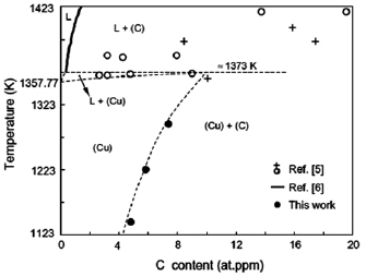
Figure V.1. Cu–C Equilibrium phase diagram at the Cu rich side, L is for Liquid Ref. [790].
Download figure:
Standard image High-resolution imageThe graphene growth process on Cu surfaces to first order can be described by the following steps, [784, 786, 791–794]:
- 1.Cu surface cleaning/preparation prior to loading into the growth chamber
- 2.Surface cleaning and annealing in the growth chamber
- 3.Exposure to a hydrocarbon precursor with subsequent adsorption of the same on the Cu surface
- 4.Nucleation of graphene by the dissociating CHx radicals and local supersaturation of C to form graphene nuclei
- 5.Surface diffusion of CHx radicals and attachment onto the graphene edges
- 6.Dehydrogenation of the CHx radicals attached to the graphene edges and dehydrogenation of some of the isolated CHx radicals with subsequent diffusion into the Cu
- 7.Coalescence of the growing graphene domains to form continuous polycrystalline films or single crystals.
Substrate selection, surface preparation, growth T and process are critical to achieve films that meet device requirements. Substrate surface quality, surface impurities, surface roughness and gas composition and pressure have large effects on the surface roughness, defects (Raman D-band), amount of FLG, and electrical properties. Graphene films of varying sizes, on Cu as well as other metal films have been grown in vertical single wafer cold wall reactors, horizontal furnaces [765], open continuous furnaces as well as in plasma enhanced single wafer systems [966]. Each one of these approaches requires optimization in order to achieve the desired results. Typically, growth conditions, such as reactor design, vertical versus horizontal, gas delivery system, precursor selection, heater, low versus high T growth, low pressure versus atmospheric pressure, must be considered and optimized. The aforementioned factors depend on material requirements as well as cost needed by a particular application.
Typically, graphene is grown on Cu foils [332], Cu thin film on sapphire, and bulk Cu single crystal foils [782, 794–796]. The most commonly used Cu foils are of a high-purity 99.9999% in a variety of thicknesses and sizes. In addition, oxygen [783, 791], carbon and other impurities [785] in or on Cu are have large effects on the growth mechanism. The quality of graphene will depend on the quality of the Cu surface morphology and crystallographic orientation. The surface of the metal can be improved by electropolishing [769, 770, 786] Many experiments have been performed on Cu annealing [797, 798], heating the substrate to T above the melting point of Cu,[799, 800], Cu surface oxidation, [786, 790, 802], using Cu with controlled crystal orientation [786] and oxygen free Cu [791]. Growth of graphene on bulk single crystals or single thin films of Cu would be advantageous. It would be ideal to grow high quality graphene directly on a dielectric surface Ref. [802] diffused C on thin Cu on SiO2 to grow graphene directly on the dielectric surface. However, at the films grown using this process are still not of high enough quality to compete with films grown directly on the metal surface. For a more extensive discussion on the growth of graphene on dielectrics, see section V.3.
Growth of graphene on Cu metal has been carried out in horizontal tube furnaces [765] as well as in cold walled single wafer tools [766, 803] and even at higher T [799, 804] than the Cu melting point, 1084 °C, using any one of several hydrocarbons (such as methane or ethylene), ethanol hydrogen and argon are also used [799, 804]. The effect of the H2/CH4 ratio on the shape of graphene domains has been widely reported [786, 800, 801]. Low pressure CVD with very low precursor flow rate has been effective in growing large area graphene filmsVarious other methods of heating the substrate have been use in addition to resistive heating, such as magnetic inductive heating [805] and a hybrid process combining hot filament and resistive (thermal) heating [806], but these techniques have not been widely adopted yet. Growth has also been carried out in the presence of a plasma in an attempt to reduce the growth T well below 800 °C.
A typical growth procedure is shown schematically in figure V.2. Prior to growth high purity Cu substrates (foils) having a thickness ranging from 25 to 35 µm and of a desired surface area are procured. The are then cleaned in acetic acid for ~10 min and then transferred in de-ionized water for additional 10 min and dried with N2. After, the Cu foil is introduced in the growth chamber and the chamber is evacuated and back filled with H2 to a desired pressure. CH4 and H2 are usually circulated to purge the lines (50:50 sccm) at pressure <4 mbar prior to substrate heating. The chamber T is then increased to 1000 °C under 20 sccm of H2 in 70 min (see figure V.2 upper frame). T is then kept constant at 1000 °C for an additional 30 min. During this last step, the Cu substrate T and microstructure are stabilized. Heating of the Cu foil to the growth T can be performed also in Ar and then in H2 gas flow at a pressure <100 mbar. The purpose of this step is to promote grain growth of the Cu foil. A 'standard' graphene growth process follows: 5 sccm of CH4 or C3H8 are then flowed for several minutes (typically ~30 min), after the growth phase, the substrate is cooled to RT by translating the furnace away from the substrate. The cooling can be done with the precursor flowing, hydrogen flow or under vacuum. The ambient during cooling is also critical especially in cases where the base pressure of the chamber is too high. In this case leaking oxygen can etch the graphene at the highest T. Once T is near RT, the gasses are closed off and the chamber is evacuated and back filled with an inert gas to one atmosphere. Growth of graphene on polycrystalline Cu foils using this process flow usually yields films with a grain size ~10 µm. By applying a longer annealing time, higher T, lower pressures, and by maintaining optimal hydrocarbon flow or melting the Cu, the domain size can reach several millimeters [807]. The lower frames in figure V.2 illustrate that domains ~800 µm can obtained systematically optimizing the CVD growth conditions and also show the corresponding Raman spectrum.
Figure V.2. (Upper) Schematic diagram of the thermal profile during graphene growth, type of gasses used and steps duration in case of growth SLG at 1000 °C, (Lower Left) Optical image of a graphene domain grown on molten Cu on a Mo substrate. Scale bar is 100 µm. (Lower Right) Raman spectrum of a graphene grown on molten Cu.
Download figure:
Standard image High-resolution imageOptical microscopy with Nomarski contrast, i.e. differential interference contrast (DIC) microscopy, is very useful (see figure V.3) to explore the quality of the Cu substrate surface as well as the grown graphene. DIC microscopy can expose cracks and micro-holes in the graphene layer and can provide information on microstructural changes before and after anneal that can be correlated with graphene film quality.
Figure V.3. Optical images of (a) continuous and (b) discontinuous graphene films on Cu.
Download figure:
Standard image High-resolution imageRaman spectroscopy has been demonstrated to be the best characterization technique to confirm the presence of SLG on the Cu substrates [1748]. The technique is introduced in section IX.2.1, where representative spectra of SLG, BLG, etc are also given. Measurements performed by SEM plotted in figure V.4 can identify dark areas interpreted as adlayers of graphene. In addition, wrinkles formed during cooling from high T because of the large difference in the coefficient of thermal expansion between graphene and Cu are also visible as narrow lines criss-crossing the surface of the graphene. If Cu of lower quality (purity 99.9% or 99.999%) is used, e.g. Cu_5N and Cu_3N, the films are heterogeneous mainly in terms of their thickness. In figure V.4 light grey color represents areas with SLG.
Figure V.4. SEM images of graphene layers on (a) Cu_mono, (b) Cu_6N, (c) Cu_5N and (d) Cu_3N substrates. Scale bars are 1 µm.
Download figure:
Standard image High-resolution imageAtomic resolution images of graphene on Cu as measured by STM (see section IX.1) presented in figure V.5 show the configuration of the carbon atoms in SLG. The corresponding Fourier transform of the STM image (upper right inset) indicates that the maxima correspond to the pattern formed as a result of the orientation of the SLG in relation to the substrate (lattice mismatch). The figure V.5 shows an area 3 × 2.2 nm with a graphene unit cell drawn upper left inset) exhibiting a lattice constant of 2.44 Å [812]. The shape, orientation, edge geometry, and thickness of CVD graphene domains can be controlled by the crystallographic orientations of Cu substrates [1749]. At the inception of the growth phase, during the nucleation stage, the Cu roughness plays a key role. The Cu-active sites are imperfections on the Cu surface, such as grain boundaries, irregularities or areas of coarseness, or surface impurities. It is at these defects that most of the graphene nuclei are formed. The higher the density of nucleation sites, the smaller the size of the graphene domains. The density of these grain boundaries is expected to affect electrical, chemical, and thermal properties, and it is thus necessary to optimize the graphene film properties according to the application requirements [808–811].
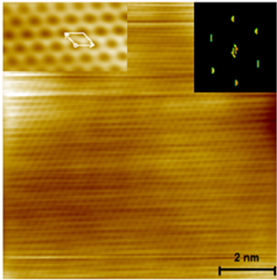
Figure V.5. Atomic resolution STM of graphene on a Cu mono-crystalline substrate with the Fourier transform (upper right inset). Adapted from [812] with the permission of AIP Publishing.
Download figure:
Standard image High-resolution imageFor some applications large (square meters) areas of graphene may be needed, as it is the case for the functional coating of large pieces of other materials. When growing graphene on 500 × 500 mm2 Cu substrates, the T uniformity across the metal substrate must be controlled since the nucleation and growth characteristics has a large T component [755]. The control of the Cu metal foil T is critically important when growing films at T close to the Cu melting point as shown in figure V.6, where part of the Cu foil melted at the edges, due to an uneven T distribution across the Cu film. Ref. [794] reported the growth of 5 × 50 cm2 single-crystal graphene on industrial Cu foils. They first transformed industrial polycrystalline Cu foils into single-crystal Cu(1 1 1) by thermal annealing using a T-gradient-driving technique. Then graphen grains growon the Cu(1 1 1) substrate and seamlessly mergeto form a large single-crystal graphene film.
Figure V.6. Higher T near the edges of the substrate causes local Cu melting while the inner part is unaffected.
Download figure:
Standard image High-resolution imageThis technique allows the synthesis of large-size single-crystal graphene films, with superior properties for various high-end applications, especially in electronics, such as large-scale fabrication of THz devices and transparent conductive film to replace ITO. It will also enable the growth of various other single-crystal LMson graphene
There are many alternatives for substrate heating, ranging from magnetic inductive heating [805] to hybrid processes, combining hot filament and resistive (thermal) heating [806]. Among them, photothermal heating (PT-CVD) provides up to 100 °C min−1 heating and cooling rates [767, 772] while keeping the chamber walls cold. The system is based on a halogen lamp-heated rapid thermal processing (RTP) (for up to 300 mm wafers), where gas lines (CH4, H2 and Ar) and their mixing manifolds are incorporated. While keeping the RTP chamber walls cold. This, together with the fast growth process, less than 1 min, helps to reduce the contamination from the walls. In this case, the cleaned Cu foil is placed between two silica plates on a photothermally heated Si- or SiC-coated graphite susceptor. Silica is needed between Cu and Si to prevent reactions between them. The growth process starts by annealing the Cu foil for 5 min at ~935 °C (as measured by a pirometer) and pressure ~7–20 mbar. Next, CH4at a flow rate of 15 sccm (CH4/H2 mixture 4:1) is introduced into the chamber. Under this condition a continuous SLG film is grown on Cu in a few tens of seconds, one order of magnitude faster than in thermal CVD using similar growth parameters. The SLG coverage is ~94% in films grown in 60 s at 950 °C. The SLG contains very small adlayer flakes, and defects (~3 × 107 cm−2) [775, 813]. The light from the RTP lamps enhances the catalytic effect of CH4 on the Cu surface without generating defects. The grain size is in the µm range. Ref. [773] reported a rapid thermal CVD (RT-CVD) suitable for mass-production. In this setup, Cu foils are loaded vertically in the reactor, in which 24 lamps heat vertical graphite receptors around the Cu foil. They obtained a growth rate 7 times higher than thermal CVD using hydrogen-free N2 carrier gas [773].
It would be desirable to grow graphene at low T for ease of process, equipment, contamination, as well as potential substrate melting issues. Ref. [814] reported growth of graphene on SiO2/Si, plastic and glass at close to RT (25–160 °C). However, in most cases the reported reduction in growth Tg/Tmp(C) is very small (⩽0.30) and for most materials the quality of the grown crystals is higher when the growth T is close to the melting point. There have been some reports on the growth of graphitic films at low T by CVD [815], plasma assisted [816] and from solid sources [814, 817] on or under Ni films but not on Cu. Growth at low T on Cu, Ni or Cu-metal alloys could be of great interest, but the grown graphene could contain many defects, as in the case of low T crystal growth of many other electronic and optical materials.
V.1.2. CVD growth of large graphene single crystals
As in the case of crystalline semiconductor materials, it may be advantageous to grow single crystal graphene films in order to minimize scattering effects by pure grain boundaries and grain boundaries that may react with ambient species such as OH, hydrocarbons, etc. Also, the presence of grain boundaries and their tilting has been studied in relation to the mechanical properties of the synthesized graphene [811].
Graphene has been demonstrated to grow on Cu surfaces by a nucleation and growth mechanism [765, 781, 818] predominantly by a surface limited process, because of the low solubility of C in Cu. The films grown using this process are polycrystalline, with a grain size that depends on the specific growth process conditions and they can range from less than one micron to hundreds of microns. Therefore, in order to increase the grain size, one would have to reduce the nucleation density on the surface of the metal. Various approaches were developed to achieve this, such as reducing precursor flow by using a Cu pocket [128, 766, 819, 820]. An example of such pocket is shown in figure V.7(a).

Figure V.7. (a) Cu 'pocket' enclosure. (b) Enclosing flat Cu foil with a quartz cover. (c) growth of graphene on Cu assisted by a continuous oxygen supply. Adapted from [766] (© IOP Publishing Ltd) and [825] (© Springer Nature).
Download figure:
Standard image High-resolution imageThe growth of large graphene single crystals led to the demonstration of very high µ in CVD graphene comparable to that of mechanically exfoliated flakes [821]. This is an important result since it has led to focused efforts on further understanding of the graphene single crystal growth as well as transfer [807, 822–824].
Further reduction of graphene nucleation density was investigated by Ref. [783, 791], who showed that graphene single crystals on polycrystalline Cu of over 1 cm could be grown after treating the surface of Cu with oxygen. However, this process is time consuming, growth times of over 10 h were used to grow 1 cm single crystals. Oxygen not only passivates the Cu surface, leading to reduced nucleation density, it also significantly speeds up the growth of graphene crystals by changing the growth regime from diffusion to edge-attachment-limited. A further explanation on the decrease of the nucleation density on the surface of Cu was provided by Ref. [785], where they observed that the surface and the bulk of the Cu foils may be contaminated with impurities including C which can aid in the formation of graphene nuclei. In this case, Cu oxidation prior to graphene growth removes carbons from the Cu surface leading to a lower nucleation density. Following the Refs. [791, 826], Ref. [825] used a solid source of oxygen, AxOy —e.g. SiO2/Si, to provide a continuous source of oxygen under the Cu substrate while providing the hydrocarbon precursor at atmospheric pressure (see figure V.7(c)). This process led to a growth rate~60 µm s−1 instead of~0.3 µm s−1 of Ref. [791]; this is a major improvement. Another approach to reducing the graphene nuclei density on the Cu surface was performed by treating the surface with melamine [827]. This process led to the growth of 1 cm graphene domains with µ reaching 25 000 cm2 V−1 s−1 for graphene transferred onto SiO2/Si. Another method was proposed taking advantage of the residual oxygen in the CVD furnace for increasing the graphene domain size beyond one millimeter, and simultaneously promote recrystallization of a polycrystalline Cu foil in the (1 1 1) structure through a peculiar 'abnormal grain growth' mechanism [828]. The process yields aligned high-quality graphene single crystals smoothly merging together, with a crystal alignment maintained over few centimeters (in 1 hr).
In general, the following critical conditions should be met in order to grow large crystals: (1) suitable substrate, (2) substrate surface cleaning and polishing prior to loading in growth chamber, (3) surface pre-treatment (oxidation, the use of melamine or other surface treatment), (4) enclosing the sample to limit precursor flow, and (5) a non-reducing surface treatment at high temperature prior to growth.
Substrate preparation is a very important first step in order to create a clean and flat surface. Many approaches can be found in literature [583, 819] on mild surface etching using acidic solutions [791, 820, 829]. However, the most reproducible surfaces have been prepared by electropolishing [766, 807]. The solution used for electropolishing has a volumetric composition of 45% water, 25% phosphoric acid, 25% ethanol and 5% isopropanol. To increase viscosity, 0.5% (weight) of urea is added. Electropolishing is performed by applying a voltage between the sample (anode) and a Cu plate cathode. A typical electropolishing procedure is 30 s at 12 V, with a cathode-anode distance of 4 cm. To ensure homogeneous polishing, it is important to keep the electrodes parallel. For this one can employ a Coplin glass staining jar as the electropolishing vessel (figure V.8(a)), which has grooves to keep the foil and the counter electrode in place, figure V.8(b). Following the electropolishing, it is important to rinse the samples under running DI water to completely remove the viscous electrolyte, followed by a quick rinse with isopropanol. Finally, the samples are dried with compressed nitrogen.
Figure V.8. Electropolishing set-up. (a) Three-quarter view. (b) Side view, showing the parallel orientation of the copper foil and the counter-electrode. Adapted from [766], © IOP Publishing Ltd.
Download figure:
Standard image High-resolution imageOwing to the catalytic nature of the Cu surface, it is important to reduce the carbon precursor flow impinging on the sample in order to reduce the nucleation density [755]. One of the most commonly-used approaches is to grow large SLG crystals inside 'pockets' formed from Cu foil, [128, 783, 791, 819, 820]. The discovery of large graphene crystals inside a Cu pocket led to the investigation of other methods to achieve similar results, for example a Cu tube [807], a sapphire cap over the Cu surface to minimize evaporation and the 'hydrocarbon' concentration [830], or placing a quartz plate on top of a flat Cu foil at a desired distance from the Cu surface [766]. The process conditions to achieve the largest single crystals will have to be optimized and perhaps combined with the use of Cu single crystals. Ref. [796] reported a comprehensive study of the evolution of the crystal morphologies grown inside Cu enclosures as a function surface orientation, absolute pressure, hydrogen-to-methane ratio (H2:CH4), and nucleation density At low pressure and low H2:CH4, circular graphene islands initially form. After exceeding ~1.0 µm, Mullins-Sekerka instabilities [1750] evolve into dendrites extending hundreds of micrometers in the 〈1 0 0〉, 〈1 1 1〉, and 〈1 1 0〉 directions on Cu(1 0 0), Cu(1 1 0), and Cu(1 1 1), respectively, indicating mass transport limited growth. Increasing H2:CH4 results in compact islands that reflect the Cu symmetry.
The nucleation density and growth rates are affected by the growth pressure and gas flow rates. While low pressure can help to radically reduce the nucleation density, it can also lead to extremely slow crystal growth. With a gas flow of~1 sccm CH4, 900 sccm Ar and 100 sccm H2, the graphene nucleation density is on the order of several crystals per mm2 and typical growth rates are ~15 µm min−1, allowing the synthesis of 1 mm-sized crystals in ~1 h. The use of Ni–Cu alloys will enable much higher growth rates due to the higher catalytic activity of Ni [831]. Figure V.9 illustrates the effect of using a nonreducing atmosphere and sample enclosure on oxidised Cu.
Figure V.9. Nucleation density of graphene when using (a) hydrogen annealing, (b) argon annealing (c) argon annealing and sample enclosure. Adapted from [766], © IOP Publishing Ltd.
Download figure:
Standard image High-resolution imageWhen hydrogen annealing is used, the nucleation density is ~10 000 cm−2 (a). Annealing in an Ar atmosphere reduces the nucleation density to ~1000 grains per cm−2 [128, 791]. Substrates annealed in argon and placed inside an enclosure have a nucleation density ~10 grains per mm−2 or lower, enabling the growth of large crystals. Figure V.10 shows a schematic diagram of the graphene growth process in a pocket and the image of a graphene single crystal grown inside the pocket. The interface between SLG and Cu (1 1 1) oxidises under ambient conditions within a few days, making SLG visible and decoupled from Cu. This is required for a reliable dry pick-up using h-BN [832].
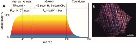
Figure V.10. (a) Typical growth scheme for a low pressure CVD process for SLG on Cu. (b) Optical dark field microscopy image of SLG on Cu foil using the process depicted in (a). Panel (B) is adapted from [832], with permission from AAAS.
Download figure:
Standard image High-resolution imageThere have been many observations on the shape of graphene domains on different Cu grains having varied crystallographic orientation [786, 1751]. The shape varies depending upon the Cu orientation as well as the growth conditions and Cu oxidation state [755, 791]. It has also been reported that growth of graphene domains on oriented Cu(1 1 1) foils [794] and Cu(1 1 1) thin films on sapphire [830] under certain process conditions are aligned. As the domain growth progresses, the domains merge to form single crystals as the Cu surface becomes fully covered by a boundary-free stitching. This is true in the case where the domains are aligned and the Cu surface is nearly atomically flat [583, 833]. The advantage of this process, if large area Cu(1 1 1) films or foils are available, is that the growth time can be significantly reduced in comparison to the single nuclei approach. Efforts have been dedicated to the growth large Cu single crystal foils [833] and [831]. More recently, a gas-flow-driven aligned growth of graphene on liquid Cu has been achieved [834]. Another method of preparing large area Cu(1 1 1) crystals is to take advantage of the epitaxial nature of Cu on c-plane sapphire and thicken the thin film using an electrodeposition process, after which Cu(1 1 1) can be peeled off from the sapphire substrate [835]. Significant activities are ongoing to optimize the growth of graphene on controlled Cu surfaces in an effort to grow high quality crystals in production worthy growth systems [836].
It would be advantageous to be able to grow single crystal graphene from a single nucleus as for bulk single crystals. Wu et al [837] used Ni–Cu alloys to increase the catalytic activity in conjunction with a localized precursor delivery technique to grow graphene single crystals over 3 cm in diameter. The growth mechanism of graphene on Ni–Cu is more complex than on Cu or Ni and further development would require precise composition identification/selection in order to ensure single layer growth and full coverage by a single graphene grain. Ref. [838] reported the synthesis of single-crystal-like SLG on polycrystalline substrates. The method relies on 'self-selection' of the fastest-growing domain orientation, which eventually overwhelms the slower-growing domains and yields a single-crystal continuous film.
In summary, the growth of high quality, large area, single crystal graphene can be performed in several ways on:
- (1)Growth on conditioned Cu substrates (oxidized or treated with melamine) under low pressure conditions (slow growth rates, size up to 1 cm)
- (2)Growth on Ni–Cu substrates with a localized precursor delivery (relatively high growth rates)
- (3)oriented single crystal Cu(1 1 1) foils
- (4)thin Cu(1 1 1) films on sapphire substrates
- (5)thick predominantly Cu(1 1 1) on sapphire followed by a peeling process so as to facilitate sapphire re-use.
V.1.3. CVD Deterministic seeded growth on Cu
Seeded graphene growth was reported by Ref. [839] patterned and etched CVD graphene patches were used as nuclei for the subsequent single crystal graphene growth. However, because of the polycrystalline nature of the starting graphene film, the resulting crystallites were not aligned but each crystal was hexagonal. In a subsequent study [840] pre-annealed foils were patterned with arrays of crosslinked PMMA, then used as a carbon source for the growth of single-crystal arrays. In both cases the array periodicity was ~20 µm and crystal size of up to ~15 µm. Due to the much lower nucleation densities required for large-crystal graphene, carbon-based seeding was found not to be robust enough for controlled growth of large-periodicity arrays. Metallic nucleation seeds were chosen instead for large-crystal graphene arrays. Ref. [841] used Cr as the nucelation sites for localized single crystal growth of graphene.
The nucleation seeds can be patterned by performing optical lithography on electropolished Cu using positive photoresist, followed by thermal evaporation of 25 nm Cr and lift-off in acetone. Cr was chosen because of its high melting point [1752], ensuring that thin films are not evaporated during the annealing of the foil and instead form particles that can act as nucleation points on passivated Cu. Spots with a diameter ~5 µm and a thickness ~25 nm lead to the most reproducible results [841]. Smaller seeds or lower film thickness did not ensure reliable seeding, whereas larger spots were sometimes found to initiate the nucleation of several separate crystals. By changing such flow ratio, it is possible to control the presence of residual Cr seeds during the growth by changing the CH4:H2 flow ratio. After growing graphene using a H2:CH4 ratio of 20:1, particles of Cr are found at the centre of seeded crystals, whereas when using a H2:CH4 ratio of 100:1, Cr seeds are removed. Growth was carried out in a 4-inch Aixtron BM Pro. All gases used in the CVD process had purities of 99.9999%. As shown in figure V.11(a), arrays with a periodicity of 200 µm show high nucleation control, with less than 10% of non-seeded nucleation. At larger periodicities (see figure V.11(b)), sporadic nucleation was slightly higher. Well-ordered arrays of crystals with a diameter of several hundred microns can be synthesised [841].
Figure V.11. Seeded arrays of large-crystal graphene. (a) Array with 200 µm periodicity and 100 µm crystal size. (b) Array with 500 µm periodicity and 350 µm crystal size Adapted from [841].
Download figure:
Standard image High-resolution imageWe now discuss the growth of single crystal graphene with controlled edge structure. Two types of graphene crystals have been grown: (1) dendritic, and (2) hexagonal [791]. The shape of the graphene crystals was controlled by the presence (dendritic) or absence (hexagonal) of oxygen on the surface of the Cu for low pressure CVD. Ref. [842] reported the growth of 100 µm hexagonal graphene crystals on polished Cu foils at one atmosphere, with limited carbon flow, with the crystal edges dominated by the zigzag direction. Controlling the graphene edges may be important for some electronic applications and growth conditions to optimize quality and growth rate(cost) should be investigated. Another important point is the growth of edge-controlled graphene in the smallest dimensions (nm scale) and the treatment of graphene after patterning and etching to set the edge structure.
V.1.4. Low pressure & low temperature CVD
It is desirable to grow film at low T not only because of the integration device flows, but also to overcome problems associated with substrates like Cu. One issue with CVD of graphene on Cu from CH4 is that the optimum growth conditions are typically at T > 1000 °C, very close to the Cu melting point of 1084 °C or even above its melting point. Cu has a vapor pressure ranging from 8.1 × 10⁻⁸ atm to 5.7 × 10⁻⁷ atm for the T range ~ 1000 –1084 °C [843]. During annealing and graphene growth at low background pressures a measurable amount of Cu is transported by the flowing gasses away from the Cu surfaces. The presence of Cu on the surface of the quartz tubes in the case of a furnace or the metal surfaces in the case of cold wall reactor can make the cost of ownership high, since the growth systems has to be cleaned on a regular basis to prevent Cu deposits flaking and particle formation. As a result there have been several activities to (1) reduce the growth T to address the evaporation and the potential integration of graphene directly in a device flow and (2) finding alternative metals or alloys as discussed above to minimize the Cu evaporation problem. It should be added that the cost and reliability of precursor delivery systems should also be considered when designing a CVD. in order of preference, gases are preferred over liquids and liquids are preferred over solids. In an effort to reduce the growth T researchers have used liquid precursors such as alcohols [844], or aromatic molecules, such as hexane [845, 846], benzene [847] and toluene [848]. In the case of benzene, high quality mostly monolayer graphene was synthesized at 300 °C with µ of 2500 cm2·V−1·s−1 by APCVD [849]. Evaporation of the catalyst was avoided and oxygen removed from the deposition chamber to minimize contamination or structural disorder of the film. Deposition of graphene at 100 °C was observed by this method but with lower quality [1753]. With extended time deposition, BLG or TLG started to form, indicating that the synthesis is not self-limiting [817]. At 160 °C continuous graphene films of reasonable quality (µ~667 cm2·V−1·s−1) were deposited on SiO2, however N was barely controlled. At lower T (from 60 to 160 °C) the deposition of continuous films was not achieved, being the coverage from 60% to 98% and the grain size and quality of the deposits deteriorated. At 60 °C on glass and PMMA the Raman signal showed the deposition of highly defective graphene layers with nanometric grain size.
Thus, the quality of the films is inferior to that grown on Cu at higher T using CH4. In addition, the delivery system for the liquids may be more complicated and more costly, not to mention the toxicity issues. Ref. [850] reported on the CVD growth of high-quality, large-area predominantly SLG films with domains o~1 µm2 and FWHM(2D)~35 cm−1 on Cu foils using C2H4at 850 °C. Spectroscopic and electrical measurements show that these films display high uniformity and crystalline quality with reasonable µ~1000 cm2 V−1 s−1 [850]. Figure V.12(a) shows the average Raman spectrum of a ~20 × 20 µm2 area (red) and a discrete spectrum taken at the centre of a SLG domain. I(2D)/I(G) is lower for the averaged spectrum as this includes the regions of secondary island growth. Figure V.12(b) plots a I(D)/I(G)map with brighter areas corresponding to regions of higher defect levels, highlighting the low defect levels throughout the film. The defects that are present here are attributed to domain boundaries. Figure V.12(c) plots FWHM(2D) across the same area of the film with brighter regions corresponding to wider FWHM(2D). The majority of the film FWHM(2D) ~35 cm−1, typical of SLG [96, 105].

Figure V.12. Raman spectrum at the centre of a SLG domain (black) and averaged across a 20 × 20 µm region of the film (red). (b) I(D)/I(G)map. (c) FWHM(2D)map. Adapted from [850], with permission from Elsevier.
Download figure:
Standard image High-resolution imageFurther characterization was carried out by fabricating GFETs. Al2O3 pre-patterning of the Cu foil passivates the areas, giving a patterned graphene film on the final substrate. Electrical measurements were performed with source-drain voltage (VSD) ~20 mV while the gate voltage was swept to +60 V and −60 V. IDS versus VGS curves in figure V.13 give hole and electron µ~1100 and 700 cm2 V−1 s−1 at RT. These fall short of the best reported values for CVD graphene [851], due to the smaller domains (~1 µm) compared to films grown at higher T.

Figure V.13. (a) Optical micrograph of GNRs on SiO2 used for GFET devices. (b) SEM image of an individual GNR ribbon with second layer islands visible as darker spots. (c) IDS versus VGS curves for GFETs (red) as-fabricated and (black) after vacuum annealing. Adapted from [850], with permission from Elsevier.
Download figure:
Standard image High-resolution imageRef. [849] investigated the growth process of graphene at ~300 °C, using C6H6as precursor at ambient pressure. They used a pump purge process multiple times to minimize residual oxidizing species in the growth chamber and annealed the Cu substrates at 1000 °C under H2 and Ar gasses for 30 min to grow the Cu grains as well as clean the surface through evaporation of potentially damaged surfaces as well as surface adsorbates. This process produced films with 100% surface coverage, 97.6% transmittance, and µ~1900 to 2500 cm2 V−1 s−1. This may become useful for back-end-of-line (BEOL) integration of graphene.
Another approach is the use of PECVD. However, the typical quality of graphene has not been significantly better than thermal CVD. PECVD synthesis on Cu foil was reported via simultaneous removal of native Cu oxide and film growth (<420 °C) [852]. This shows the importance of smoothing Cu and the differences in the deposition on top and bottom sides. The bottom side near the sample holder suffers a confinement that allows preparing smooth Cu metallic surface and growth of mostly SLG continuous films in one step. However the process is not self-limiting and the thickness was time dependent. Contamination of the process tube with Cu affects the lifetime of furnace as well as reproducibility.
V.1.5. CVD graphene growth on Ni
Growth of graphitic carbon on Ni was achieved asfar back as the 1960s [746] and to the 1970s [753, 853]. Using PECVD, vertically oriented graphene nanosheets (VOGNs) on Ni can be prepared [854–856]. Carbon on metals is either soluble or it reacts to form a carbide. The majority of efforts on growth on metals have focussed on the use of non-carbide forming metals such as Cu, Ni, Co, Pt, Ru, Ir, and Au. There have been interesting reports on the growth of graphene on carbide forming as well [1754]. In this section we focus on the growth of graphene on Ni and Co, and similar metals. The solubility of C in Ni and Co is fairly high in comparison to that of C in Cu [857, 858], and it is much higher than that in Cu [790] ~1 at% (C in Ni) versus 8–10 ppm (C in Cu). The higher solubility makes it difficult to grow uniform SLG on the metal surface [756, 761]. In both growth on Ni and Co, one can grow produce patchy SLGs. Even by decreasing the Ni or Co thickness and growth T, single layer control is very challenging. This also does not solve the equivalent challenging problem of coefficient of thermal expansion difference between metal and graphene [859].The growth of graphitic C on Ni, Co, Pt and other elements that have high C solubility occurs principally by a diffusion and precipitation mechanism from the bulk of the metal [753, 754, 788]. Depending upon T and microstructure the C diffusion can be dominated by grain boundaries or bulk diffusion. Ref. [781] showed using C isotope labeling that while in the case of Cu, graphene growth is dominated by surface growth, on Ni this takes place by dissolution followed by diffusion and precipitation upon cooling to RT. Growth on Ni and Co alloys of Cu on the other hand has given better results, including growth of large area single crystals [1755]. This is due to a number of reasons, the principal being that at low Ni concentrations in Cu, the catalytic activity of the metal surface is much higher than just on Cu, leading to a higher surface growth rate [837]. While growth on elemental Ni and Co resulted in uncontrollable graphene layers, growth on Cu alloys (Ni_Cu, Co–Cu, etc) may lead to controlled larger single crystals of graphene [837]. The presence of metals with higher catalytic activity could also enable growth at lower T.
V.1.6. CVD growth on metal foams
The integration of graphene into accessible and scalable 3d materials is an issue that is inspiring a growing field of research [860]. Free-standing interconnected porous graphene materials, called graphene foams (GF), attract interest due to their ability to transfer many of the unique properties of graphene to a larger scale, with high surface area >850 m2 g−1 high electrical conductivity (>10 S cm−1) and good structural integrity, retaining the form of the metallic template on which they were synthesized [861]. Applications include variable geometry elastic conductors [861], lithium ion batteries [862], EMI shielding [863], supercapacitors [864, 865] and lithium sulphur batteries [866, 867].
Structures such as papers [542] and hydrogels [343] can be prepared starting from chemically exfoliated graphene and/or GO [304]. These often suffer from poor electrical conductivities (e.g. only 5 × 10⁻³ S cm−1) [343] and thermal properties, mainly because of defects and their non-continuous nature. Graphene may be grown on templates of virtually any shape by CVD and continuous structures can be obtained starting from custom porous templates. Synthesis of graphene foams by CVD on metal foam templates was reported in Ref. [861]. The authors used commercially-available Ni foam templates to fabricate tunable, macroscopic structures consisting of high quality interconnected graphene sheets. The resulting materials were highly conductive, light and flexible with high surface area, and subsequent infiltration with PDMS led to robust composites that exhibited a resistance change when subjected to mechanical deformation, such as bending or stretching, indicating their potential in the field of stretchable electronics. This work inspired a lot of new research around graphene foams, for many different applications, such as lithium storage [347], high sensitivity detection of NH3 (ppm in air at RT and NO2)[868] supercapacitors [869], conductive scaffolds for the proliferation of neural stem cells [870], superhydrophobic coatings [871] combined with Teflon, or stretchable strain sensors [872] combined with PDMS.
The growth process depends on the metal catalyst. In the case of Cu, the process is self-limited, i.e. growth mostly ceases as soon as the Cu surface is fully covered with graphene principally because of the negligible C solubility and C diffusivity in Cu [781]. In the case of Ni, the carbon atoms diffuse into the bulk of the metal due to the high carbon solubility, ~0.9% at 900 °C [781], and graphene is formed both by the isothermal growth on the surface and carbon precipitation from the bulk upon cooling [115]. The shortcoming of graphene growth on Ni is the poor control on N, which is strongly influenced by the Ni thickness, T and exposure time to the hydrocarbon, and the cooling rate, not yielding uniform SLG but rather FLG [791]
In Ref. [873] GF were grown on commercially-available Ni foam templates by CVD in a hot-wall tube furnace (diameter 5 cm) using CH4. The templates were washed by ultrasonication in dilute hydrochloric acid, then de-ionised water, and finally acetone, before being placed inside the furnace and heated to 1000 °C under a H2 flow of 50 sccm. After annealing under these conditions for 30 min, the flow of H2 was increased and CH4 introduced (H2:CH4 = 500:50 sccm). Following a 10 min deposition time, the sample was removed from the furnace and allowed to cool in flowing Ar or N2 for at least 2 h. To remove the sacrificial Ni templates, the samples were immersed overnight either in 17 vol% nitric acid (HNO3) or in 4.5 vol% iron (III) chloride (FeCl3) followed by 10% hydrochloric acid (HCl) heated to 80 °C. Finally, they were thoroughly rinsed in deionised (DI) water then allowed to dry completely before further handling.
Figure V.14 shows the characterization of the synthesized GF. From SEM observations, the wall thickness is estimated to be 10–20 nm, characteristic wrinkles are observed in the foam, arising from the mismatch in thermal expansion coefficients between Ni and graphene [874].The interior is hollow, indicating that Ni etching was successful. XRD measurements on foams etched with HNO3 showed residual Ni (figure V.14(g)), most likely due to the produced by the reaction of Ni with HNO3. These gas bubbles could block the infiltration of etchant to some channels of the internal structure. To overcome this, etching was instead performed in FeCl3, which has no gaseous products on reaction with Ni, only soluble salts. These were [873] washed away in hot HCl, which also served to complete the etching process. XRD measurements confirmed that the resulting GF had few traces of Ni when FeCl3 was used at RT (figure V.14(g)), and no traces of Ni when it was at 80 °C. However, in this case there was some residual Fe (figure IV.14(g)).

Figure V.14. Characterization of GF from Ni foam precursor. SEM images of (a) Ni foam as received, (b) and (c) GF. (d) Photographs of foam at different stages of the synthesis process. (e) TEM image of GF. (f) Electron diffraction pattern from the foam area in (e). (g) XRD patterns of (i) Ni foam, GF etched with (ii) HNO3, (iii) FeCl3 followed by hot HCl and (iv) hot FeCl3 followed by hot HCl. (h) Raman spectrum of GF, adapted from [873], with permission of Springer.
Download figure:
Standard image High-resolution imageTEM diffraction measurements confirmed the polycrystalline graphite nature although the thickness of the walls was too large to observe the individual layers of graphene (figures V.14(e)–(f)). The quality of the sample was further investigated by Raman spectroscopy (figure V.14(h) The small D peak indicates negligible defects. The 2D is consistent with that of FLG. Thinner GF featuring fewer layers of graphene may also be grown by varying parameters such as the amount of CH4, the growth time and/or T and the cooling rate. However, thinner foams are less robust and require a PMMA support during etching, so that they do not collapse [861].
The structures described above are limited by the commercially-available templates, which typically have pore sizes in the range of 200–400 µm. In this case, most of the volume is occupied by void space rather than graphene, which is a disadvantage in applications such as energy storage, where a high volumetric energy density is required. Thus, a smaller pore size is often desirable.
High density scaffolding have been produced, as described in [875] as follows: Ni and Cu metal powders with typical particle sizes between 0.5 and 150 µm were purchased from Sigma Aldrich (figure V.15(a)). In the case of Cu powder below 1 µm, the powder was additionally mixed with MgCO3 powder to prevent the agglomeration of the metal particles and compressed. The powder was placed into a quartz combustion vessel inserted into a quartz tube in a horizontal tube furnace. An annealing step with a flow of 400 sccm argon and 100 sccm hydrogen at high T for 45 min was used to connect the metal particles (thus forming the metal scaffold, see figure V.15(b)) as well as to remove metal oxides and contamination. The minimum T for preparing the scaffold was 600 °C for Ni and 800 °C for Cu. Carbon feedstock was provided by a CH4 flow of 10 sccm under a constant Ar flow of 400 sccm and a total pressure of 50 mbar and 400 mbar for the case of the growth on Ni and Cu, respectively. These were the minimum pressures yielding closed graphene layers on the metal templates for all the investigated temperatures (figure V.15(c)).

Figure V.15. Fabrication principle of graphene foams illustrated by SEM images. (a) Metal particles, in this case Ni, are assembled in a vessel to get (b) a 3d structure. (c) At high T (~600 °C) interconnected metal foams are created; this process is implemented in the CVD annealing step. The scale bars are 20 µm. Adapted from [875], © IOP Publishing Ltd.
Download figure:
Standard image High-resolution imageFigure V.16(a) plots a typical Raman spectrum at 532 nm of GFs grown on Cu at 900 °C and Ni at 600 °C. This gives Pos(2D) ~2695 cm−1 and 2699 cm−1 for GFs (Cu) and GFs (Ni), respectively, with FWHM(2D) ~61 cm−1 and 80 cm−1 for Cu and Ni-grown GFs, respectively, indicating FLG. I(D)/I(G) ~ 0.16 and ~0.25 for Cu- and Ni-grown GFs, indicating defects.

Figure V.16. (a) Raman spectra of GF grown on Cu (red curve) at 900 °C and Ni (black curve) at 600 °C. (b) SEM micrograph of GF grown at 800 °C after metal etch. (c) Optical image of Ni foams fabricated at 800 °C and 1100 °C using a Ni powder. Scale bar in (b) is 20 µm and in (c) 5 mm. Adapted with permission from [873, 875].
Download figure:
Standard image High-resolution imageFor SEM analysis the GFs were freeze-dried at low pressure in liquid N2 for several hours in order to prevent the collapse of the foam. A SEM picture of a GF is in figures V.16(b) and (c) depicts an optical image of two Ni foams fabricated at different T.
A similar process was described in Ref. [873], in which a combination of Ni and NiO NPs compressed into a pellet were used as the template. Despite the presence of NiO, the mechanism for the subsequent growth of graphene did not change, since during the annealing process in a high-T (1000 °C) H2 atmosphere NiO was reduced to Ni, leading to the same behaviour as for Ni templates. After growth, the sacrificial template was removed. A long period (several days) of immersion in the etching solution was required before no more colour change was observed, indicating that all the Ni had been removed.
Figure V.17 reports the characterization of the GF produced in this way. The pellet subjected to high pressure (~440 kg cm−2) was too compact (figure V.17(a)), while the GF synthesized from pellets subjected to low pressure (~50 kg cm−2) shows a well-controlled particle size distribution (figures V.17(b) and (c)), with a network of interconnected hollow branches of graphene. The pores are in the 1–10 µm range, around 2 orders of magnitude less than the GF grown on commercially-available Ni foam templates. As estimated from the SEM images, the thickness of graphene is less than 10 nm. Indeed, by TEM, 10–30 layers of graphene could be observed (figures V.17(e)–(f)) and the polycrystalline graphite nature was confirmed as before by diffraction measurements (figure V.17(g)). To analyze the quality of the graphene, Raman spectroscopy was employed at 632.8 nm (figure V.17(d)). The sample was first fragmented slightly to ensure that measurements were taken from the inside of the foam. No significant D peak was visible in the Raman spectrum, indicating negligible defects and the 2D peak was consistent with FLG.
Figure V.17. (a) SEM image of GF from pellet of Ni/NiO NPs pressed under ~440 kg cm−2. The resulting pellets are too compact, with only small areas of porosity where NPs resist tight packing. (b) and (c) SEM images of the GF from pellet of Ni/NiO NPs pressed under ~50 kg cm−2. (d) Raman spectrum from HD-GF sample. (e) and (f) TEM images of the HD-GF foam. (g) Electron diffraction pattern from the area in (f). Adapted from [873], with permission of Springer.
Download figure:
Standard image High-resolution imageV.1.7. CVD growth of graphene on metal alloys
Selection of the proper alloy could address some of the shortcomings of Cu. Ref. [876] studied the use of Mo-Ni alloys to grow SLG without the precipitation of diffused C into the bulk, because Mo traps C by forming a Mo-carbide. In principle, this approach could be extended to other metal alloys with the objective of finding a substrate with better CTE matching with graphene than Cu, and lower vapor pressure at the growth T. Another widely studied alloy is Ni–Cu in order to take advantage of the low solubility of C in Cu, the higher catalytic activity of Ni and the non-linear behavior of C solubility on Ni concentration in Cu1−xNix [857]. Additionally, some of the metal alloys could be much better catalysts than Cu, enabling growth at much lower T [877, 878]. Refs. [877, 878] grew predominantely SLG by an admixture of Au to polycrystalline Ni. This allows a controlled decrease in graphene nucleation density, at low T ~450 °C. The graphene films exhibit an average I(D)/I(G)~0.24 and domain sizes >220 µm2 were reported via the design of alloy catalysts.
Carbide forming metals were also suggested to to grow SLG [879, 880]. Commercially available polycrystalline groups IVB-VIB metals (Ti, Zr, Hf, V, Nb, Ta, Mo and W) were used to grow graphene by CVD at ~1050 °C. However, the Raman spectra showed many defects, as exhibited by the presence of a high intensity D-band.
V.1.8. Mechanisms of graphene CVD growth on Cu and Ni
To get some insights into the atomic mechanisms ruling the growth of on metals by CVD, understanding the specific CVD kinetics [881] is crucial for advancing graphene processing and achieving a better control of graphene thickness and properties. Although the thermodynamics of the synthesis system remains the same, based on whether the process is performed at atmospheric pressure (AP), low pressure (LP) (0.1 − 1 Torr) or under ultrahigh vacuum (UHV), the kinetics are different, leading to a variation in uniformity. Graphene synthesis using a Cu catalyst in APCVD processes at higher CH4concentrations revealed that the growth is not self-limiting, which is in contrast to previous observations for the LPCVD case [1756]. Hydrogen acts as an inhibitor for CH4 (and for other widely used precursors like C2H4) on Cu and other metals, supressing deposition onto the surface [882]. Besides, hydrogen plays a key role in forming form C—H out of plane defects (as efficient nucleation points) in CVD graphene on Cu, defining an optimal (and desired) CH4/H2 ratio [882].
Several theoretical studies predicted that carbon atoms are thermodynamically unfavourable on the Cu surface under typical experimental conditions, and the active species for graphene growth should thus mainly be CHx instead of atomic carbon [883]. Based on this [882, 883] the nucleation behaviour could be understood (see figures V.18(A) and (B)), explaining many experimental observations and providing a guide to improve graphene simple quality [883]. Other studies were conducted combining ideas from step flow growth augmented by detailed first-principles calculations [792]
Figure V.18. (a) Sketch of graphene formation by both direct chemisorption/deposition on Cu (and precipitation/segregation on Ni) [882] (with permission of the PCCP Owner Societies). (b) Computed optimized structures of representative carbon clusters along the graphene growth-by-aggregation on Cu(1 1 1) and (1 0 0) surfaces [883] (copyright American Chemical Society). (c) Evolution of graphene grown via thermal decomposition of methane on Cu(1 1 1). Top: Schematic illustration of the surface intermediates at different reaction conditions. Bottom: overview of STM images showing (C.a) carbon clusters, (C.b) the boundary between carbon cluster (left) and defective graphene (right), (C.c) defective graphene, and (C.d) vacancy-free graphene, at different reaction stages [884] (copyright American Chemical Society).
Download figure:
Standard image High-resolution imageA combination of in situ LT-STM experiments and DFT-based calculations (see figure V.18(C)), revealed the growth intermediates of CVD graphene on Cu(1 1 1) via thermal decomposition of CH4at different growth stages, comprising various carbon clusters (i.e. carbon dimers, carbon rectangles, 'zigzag' and 'armchair'-like carbon chains) and defective graphene [884]. Saturation of these carbon clusters on Cu(1 1 1) resulted in the transformation into defective graphene, with pseudo-ordered corrugations and vacancies due to lattice mismatching. These defects were healed by high T annealing in the presence of CH4 and transformed into vacancy-free SLG. Such atomic insights of the structural evolution at different stages of graphene grown on Cu(1 1 1) can help better understand the growth mechanism of CVD graphene, and provide design rules for large scale growth of single crystalline graphene films.
The kinetics of graphene growth on Cu were also studied using Raman spectroscopy taking advantage of the mass difference of 12C and 13C [781, 791] where the time dependence of graphene growth on the surface of Cu was presented as shown for oxygen rich and oxygen free Cu surfaces in figure V.19
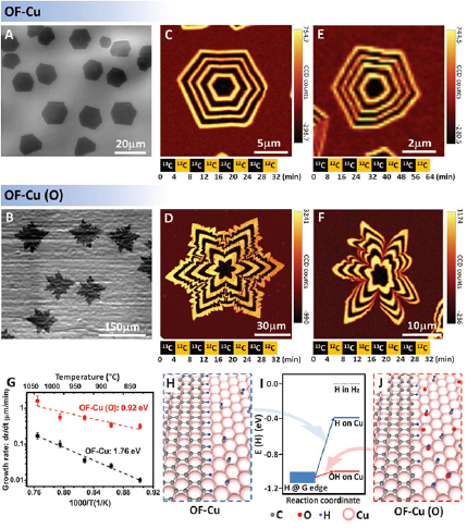
Figure V.19. Effect of O on graphene growth kinetics. SEM images of graphene domains grown on (A) OF-Cu and (B) OF-Cu (O). Isotope-labeled Raman maps of I(2D) on Si for growth at (C) and (D) 1035 °C and (E) and (F) 885 °C. The isotope switching intervals are indicated below each image. (G) Logarithmic plots of graphene domain growth rate dr/dt versus 1/T. The error bars are from calculations of different domains for each case, and the activation energy Ea is extracted from the slope of the linear fit. (J) and (H) Atomic-scale schematics of graphene edge growth on Cu with and without the assistance of O, respectively. (I) DFT calculated energies of different configurations of H attachment, in reference to H in H2. The energy spread of H at the graphene edge is due to the computational uncertainty resulting from the lattice mismatch between graphene and Cu. Adapted from [791] with permission from AAAS.
Download figure:
Standard image High-resolution imageOn Ni another interesting growth mechanism can take place. This arises from the decomposed on-surface C atoms, catalytically produced from the CVD CH4 [888] (or other precursors like C2H4, among others) at high T (see figure V.20(A)). The favourable solubility and diffusivity permits the decomposed C atoms to diffuse into the Ni bulk during the annealing stage at high T [889]. Then, the inward carbon atoms precipitate (segregate) on the catalyst during the cooling period due to supersaturation of the diluted carbon into Ni. This supersaturation-by-cooling leads to the segregation of carbon atoms on the cooled Ni surface, which will promote the formation of the graphene domains. It is worth mentioning that this mechanism has been validated by a complex theoretical computer modelling protocol accounting for a large variety factors affecting the CVD graphene synthesis (solubility in Ni, growth time, growth T, cooling rate, Ni thin film thickness, among others) [886], and will naturally lead to the formation of MLG easier than in other metal substrates by the nature of the segregation mechanism. Another growth mechanism of graphene on Ni(1 1 1) was suggested in Ref. [887] at T < 460 °C. A surface-confined nickel-carbide phase coexists with SLG (see figure V.20(B)). This grows by in-plane transformation of the carbide along a phase-boundary, unlike other growth processes on other transition metals and on Ni above 460 °C, where carbon atoms attach to 'free' edges of graphene islands [887].

Figure V.20. (A) sketch of graphene CVD growth on a Ni surface [885, 886] through the carbon diffusion and cooling processes. (B) (Top-left) the hexagonal structure of the graphene domain can be identified in the STM image, while the right side shows the quasi-square structure of the carbide Ni2C. The domain boundary between the two phases is in the same atomic plane and without any defect pattern. This indicates that the two phases form a line interface. (Top-right) the carbide and graphene lattices are superimposed in the region indicated by the rectangle in the top-left panel. (Bottom) Top and side views of the optimized atomic structure of the graphene/Ni2C interface [887] (copyright American Chemical Society).
Download figure:
Standard image High-resolution imageV.1.9. Graphene growth on noble metals
Other low-interacting substrates have been explored. Ref. [108] reported the growth of graphene on Pt. This hand high crystal quality with lowest wrinkle height ~0.8 nm and µ > 7100 cm2 V−1 s−1 under ambient conditions. The repeatable growth of graphene with large single-crystal grains on Pt is nondestructive after electrochemical delamination of the grown graphene [108]. The growth of can be designed to control the graphene edges that range from zigzag to armchair orientations via growth-etching-regrowth by CVD on Pt [782]. Ref. [890] reported the nucleation and growth of graphene islands on Pt(1 1 1) at T ~ 1000 K by CVD of ethylene. Using a CVD method followed by a repeated etching-regrowth process on Pt Ref. [891], single-crystal graphene domains were reported up to 13 000 cm2 V−1 s−1 under ambient conditions. Ref. [892] engineered the grain size of SLG grown on Pt with a limitted carbon solubility, by a segregation–adsorption CVD yielding a grain size ranging from ~200 nm to ~1 µm, which enabled the determination of the scaling laws of thermal and electrical conductivities as a function of grain size. They concluded that the thermal conductivity of graphene decreases with grain size, while the electrical conductivity slowly decreases with a small grain boundary transport gap ~0.01 eV and resistivity ~0.3 kΩ µm. CVD-graphene growth on Pt substrates can provide an extra added-value, as it may exhibit catalytic properties towards H2 dissociation [893]. Pt is one of most commonly used materials for electrodes due to its thermal stability and chemical resistance.
The thermal expansion coefficient difference of Pt with graphene is smaller than for other transition metals [894]it is possible to tune the edge termination of the crystals via growth–etching–regrowth [108, 782, 793].
Efforts have been made not only in the growth of millimetre-sized hexagonal single-crystal graphene films on Pt but also in developping transfer methodologies. A bubbling method, was used to transfer SLG grown on Pt to arbitrary substrates, using a nondestructive process not only to graphene, but also to the expensive Pt substrates [108]. There are also studies focused on the growth on other noble metals, such as Ir [895], Ru [896] and Rh [896]. Moiré patterns have been explored on graphene on Rh(1 1 1) using in situ STM [897]. The synthesis of large-scale uniform graphene films on high carbon solubility substrates of Rh foils at ambient-pressure CVD was reported [898].The thickness of graphene can be tuned from multilayer to monolayer by increasing the cooling rate in the growth process graphene prefers to stack deviating from the Bernal geometry, with the formation of moiré patterns. Ref. [899] grew SLG on Ir(1 1 1) by LP CVD. The graphene layer had a very low density of defects. These are edge dislocation cores consisting of heptagon–pentagon pairs of carbon atom rings, related to small-angle in-plane tilt boundaries. Using Ir(1 1 1) as substrate at 750 °C–900 °C, growing rotated islands are more faceted than islands aligned with the substrate [895]. Further, the growth velocity of rotated islands depends not only on the C adatom supersaturation but also on the geometry of the island edge. Different growth mechanisms were proposed to explain the differences in the graphene edge binding strength to the substrate. Graphene growth by CVD of ethylene on a Ru(0 0 0 1) surface was also explored. At low pressures and high T the metal surface facets into large terraces, leading to ordered graphene layers [900]. Engineering of Ru surfaces with Ar+ sputtering to produce subsurface bubbles led to a tailored growth of graphene on Ru(0 0 0 1) and to anysitropic oxygen interacalation [896].
V.1.10. CVD growth on Ir (1 1 1)
The substrate Ir(1 1 1)/YSZ/Si(1 1 1) in principle allows integration with Si technology. However, the growth is ruled by the outermost Ir atoms, and therefore the process may be generalized to many other transition metals like Ir [895], Ru [896] or Rh [896].
In the case of Ir and Pt, the interaction with the substrate is rather low, and this presents pros and cons. As an advantage graphene can be transferred to other substrates. However, the main disadvantage is the small domain size, as many rotational domains can be generated [901, 902]. Work is underway in the search of optimization methods for enlarging domain sizes, even to millimeter scales. Ru and Rh are substrates were the graphene-substrate interaction is very strong and it is possible to grow large grains on single-crystal substrates, however transfer is difficult [1757, 1758].
SLG on Ir(1 1 1) thin films on YSZ-buffered Si(1 1 1) wafers [903] was reported [905]. The substrate was first cleaned by Ar sputtering (0.8 keV, 5 µA, 15 min) and annealing to 900 °C followed by an oxygen treatment (p(O2) = 5 × 10⁻⁸ to 1 × 10⁻⁷ mbar, T between 400 °C and 550 °C) and a final flash annealing (to desorb the oxygen) up to 900 °C.
SLG was grown using ethylene as a precursor CVD at T = 850 °C, starting from very low ethylene partial pressures (ideally <1 × 10⁻⁸ mbar for the first 20–30 min), then progressively increasing the pressure up to 2 × 10⁻⁷ mbar. This approach prevents the formation of multiple nucleation centers, which would result in the appearance of many rotational domains (mosaicity). The substrate should first be heated to the setpoint T and only then should ethylene be admitted into the chamber[905]. Surface processes such as oxidation and overlayer (including graphene) formation modify the work function of the metal substrate, the photoelectron yield measured while irradiating the sample with a pulsed UV source can be used to track the onset of the surface process under study and to monitor its evolution until saturation is reached [905].
V.1.11. MBE growth on Pt(1 1 1)
Several physical evaporation methods employing sublimation from a carbon source have been used, like electron beam evaporator [906, 907], or a resistively-heated piece of graphite [790, 908]. The growth of nanometer-sized SLG on hBNby MBE was reported [909].
Ref. [910] used a solid carbon source consisting of a glassy carbon filament connected by two refractory metal bars to a DC current source. Thanks to a 10 times higher resistivity of glassy carbon versus graphite, it is possible to use moderate electrical current ~14–18 A [911]. This makes this method simple and easy to install in a UHV system, significantly reducing contamination. Ref. [910] showed that for MBE growth of graphene, the substrate can be at lower T than in other methods [912, 915, 916]. This enables growth on dielectric substrates in an inherent transfer free process. Also, in situ surface science analysis techniques (LEED, RHEED, STM, XPS) can be used in a highly controllable growth environment (growth rate, substrate type, substrate temperature, in situ doping).
The evaporation growth rates are generally very as low as 3 × 10⁻⁴ ML s−1 to avoid a rapid degeneration of the glassy carbon filament. This requires a sample-to-source distance of tens of millimeters. At this distance the sample is radiatively heated.
An evaporation carbon source can be fabricated [913], using a resistively heated piece of glassy carbon [914], [915].
Using a 0.3 mm thick glassy carbon plate cut in the desired shape (see figure V.21) by laser or water-jet cutting, one gets the carbon source as shown in figure V.21(b). The glassy carbon filament is mounted on a standard UHV feedthrough, terminated with Ta rods, and fixed with Mo screws.
Figure V.21. A glassy carbon filament (a) is mounted on an UHV electrical feedthough (b) and resistively heated (c). T is simultaneously measured with an optical pyrometer and a type-C thermocouple located on the back side.
Download figure:
Standard image High-resolution imageThe C Source is placed in a deposition UHV system, base pressure 1 × 10⁻¹⁰ mbar heated using a DC current. The T calibration of the cell is performed in a separate UHV system with a base pressure 1 × 10⁻⁸ mbar. The T in the hottest spot of the filament is measured using a dual-color optical pyrometer through an optical window located in front of the cell. Evaporation of carbon starts above 2000 °C. Using a DC current ~14 A (~100 W) the filament is at 2014 °C. A clear correlation of the increase of the partial pressure of atomic mass unit number 12 (a.m.u.) is observed in a residual gas analyzer (quadrupole) with source temperature. The presence of amu 12 can be associated to the evaporation of monoatomic carbon. The deposition rate is 3 × 10⁻⁴ SLG s−1.
By exposing a clean Pt(1 1 1) substrate to the carbon source the formation of carbon structures is observed [910]. First, the glassy carbon filament his held at T > 2000 °C for degassing for 15 min. The pressure is kept <1 × 10⁻⁸ mbar. Before growth, the Pt single crystal is cleaned by cycles of Ar+ sputtering and annealing at 850 °C. The cycles are repeated until a sharp LEED pattern is observed, where only Pt peaks appears and/or STM images showing clean and flat extended regions. Then, one places the Pt (1 1 1) substrate at ~650 °C in front of the carbon source at 2000 °C with a distance between them of 20 mm. After 30 min 0.5 ML SLG is attained. During the process the pressure is ~7 × 10⁻⁹ mbar. The procedure works equally well if the sample is annealed after growth. The graphene formation is demonstrated by in situ LEED and STM. The LEED diagram in figure V.22(a) shows the spots corresponding to the Pt(1 1 1) plus a surrounding ring characteristic of graphene. Brighter spots along the ring are indicative of the preferential orientations of the carbon periodicity with respect to the Pt crystal orientation. Figure V.22(b) shows an STM image measured on the graphene areas. The bigger periodicity (bright bumps) of the image corresponds to one of the possible moirés. The smaller periodicity (diagonal lines) is the atomic corrugation of the graphene. Graphene covers extended regions of the surface with a surface morphology similar to growth from decomposition of hydrocarbons or aromatic molecules.

Figure V.22. (a) LEED pattern on SLG/Pt(1 1 1). (b) STM image showing a moiré and the atomic corrugation of graphene. Adapted from [910], with permission from Elsevier.
Download figure:
Standard image High-resolution imageThe MBE growth mechanism on Pt(1 1 1) by the evaporation of C atoms can be understood on the basis that the evaporated C atoms will not interact with each other or with gases until they reach the surface. This guarantees a continuum flux of atomic C on the surface, heated up to the desired T. The synergistic effect of surface T with the kinetic energy of the C atoms reaching the surface catalyses the initial graphene nucleation by atomic on-surface aggregation: C atoms reaching the surface are free to move until finding correct (stable) positions on the surface crystal lattice to bond and the epitaxial graphene growth undergoes by aggregation of on-surface diffusing C atoms or nucleated nanostructures (see figure V.23).
Figure V.23. Sketch of the coexisting processes leading to the growth of graphene on a Pt(1 1 1) surface by MBE.
Download figure:
Standard image High-resolution imageT-assisted on-surface diffusion of C nucleation centers, able to collide with others, favours graphene formation, which will epitaxially grow in their most stable graphene domains. The CI-NEB approach [916, 917] yields a minimum diffusion barrier of a C atom on Pt(1 1 1) of 0.45 eV, and a C + C → C2 on-surface aggregation reaction barrier <0.8 eV (with a net enthalpy gain ~3 eV), to be compared with barriers of 0.6 and 1.1 eV, respectively, reported for the Cu(1 1 1) surface [918], or the 0.58 eV for the atomic O diffusion barrier on Pt(1 1 1) [919]. These energy barrier values are easy to overcome in seconds at the typical surface temperatures in the MBE process on Pt(1 1 1). In addition, the graphene epitaxial growth-by-aggregation will be favoured as the nanopatches increase their size, which will be able to stabilize the incorporation of new diffusing C atoms and larger nucleated C nanostructures.
V.1.12. MBE growth on Au
The use of Au as a substrate is difficult, since the T needed to obtain graphene is too close to Au melting point [906, 907]. A solid-carbon source can be used to decrease the T.
The Au (1 1 1) substrate is kept at 550 °C, with a well degassed carbon filament. This step can last for days because the freshly new filaments are porous containing many impurities. The degas pressure needs to be <5 × 10⁻⁹ mbar when the glassy carbon filament is at ~1600 °C (12 A, 83 W).If this step is not performed correctly, the samples get covered by an amorphous layer and the substrate has to be cleaned again.
In case of graphene growth by supersonic molecular beam epitaxy (SuMBE) from C60 [920, 921], the two major issues to take into account are the substrate type and kinetic energy (KE). The main steps are the following:
- Surface preparation. Numerous (up to 40) Ar ion sputtering (0.5 keV) and annealing cycles of the Cu substrate (T > 700 °C for optimal LEED diffraction pattern) to avoid the presence of unwanted contaminants, such as oxygen, sulphur or remaining carbons, during growth.
- Carrier gas choice. He or H2The use of noble gases prevents strong interactions between carrier gas and the substrate and does not affect C60 internal dynamics, which is frozen unlike ordinary heating that increases the molecular vibrations.
- Aerodynamical acceleration of the highly diluted (less than 1% of the mixture) C60 beam by isentropic expansion of the flux out of the injection cell into vacuum through a nozzle. By changing the carrier gas and the seeding parameters (source T, gas inlet pressure), fullerene KE can be tuned, being inversely proportional to the carrier gas mass. KE ~ 10–15 eV using He carrier gas up to 30–40 eV using H2.
- Collimation of the expanded flux and impact of the organic molecules on the Cu reconstructed surface, keeping the substrate at RT.
- Thermal activated growth of graphene islands by increasing T to 645 °C.
Refs. [922, 923] showed that substrate T must be raised to 645 °C to synthesize graphene islands as C60 high-energy deposition on Cu, even at the highest KE reachable by SuMBE, does not lead to immediate C60 cage rupture.
The ultimate evidence of the presence of defected nanometric graphene islands comes both STM and Raman spectroscopy [923]. This process is expected to be self-limiting and to stop completely as soon as the Cu surface is entirely covered by a monolayer of carbon atoms [923].
Ref. [923] reported a coating of graphene-like material at 645 °C using H2 as carrier gas. These nanoislands also contain pentagons, which come from the original buckyball structures. Thus, at this stage this is just a proof of principle approach. The technique might be applied to a wide range of substrates, such as semiconductors and insulators, avoiding transfer.
V.1.13. UHV-thermal decomposition on Cu foil, Cu(1 1 1), Pt(1 1 1) and Ir(1 1 1)
This method consists in the growth of graphene in a UHV environment, using surface decomposition of C60 [924] as a carbon source. The same method applies to Pt(1 1 1) and Ir (1 1 1), Cu(1 1 1)single crystals [901, 912, 925] and Cu foil [926].
The combination of a UHV environment together with the use of C60 molecules provides some advantages with respect to conventional CVD [927, 928]. On one hand, this procedure is self-limited, which assures the growth of SLG. On the other hand, the controlled and clean environment (UHV chamber with a base pressure ~10−10 mbar) results in samples almost free of impurities with a lower growth T than CVD.
Ref. [926] used commercial C60 (Sigma, 98% purity). To control the evaporation rate, a molecular evaporator is needed, that can be either commercial or homemade, as in this case. Figure V.24 shows a homemade one with a Ta crucible on which a type-K thermocouple is spot-welded. The molecules are placed inside the crucible. Acurrent is passed through the Cu rods and the molecules are evaporated at 450 °C–500 °C. Molecules are outgassed in UHV conditions prior to growth. To this aim, C60 is heated 10 °C above the growth T, until the initial pressure is restored (~10−10 mbar) after elimination of impurities (water, CO, CO2). Usually the crucible is spot welded to two pieces of steel that are clamped to Cu rods. It is important to have a good electrical contact between Ta crucible and rods, otherwise the whole evaporator will be heated and the result will be a rise in the base pressure of the chamber and, therefore, a dirty evaporation.

Figure V.24. Homemade C60 evaporator.
Download figure:
Standard image High-resolution imageCu, used as a substrate, is cleaned with several sputtering and annealing cycles. A standard preparation consists in five cycles of 10 min Ar sputtering and 10 min annealing by electron bombardment at 800 °C. For the first cycle the sample current is 10 µA. For the last cycle, the sample current is reduced to 5 µA to prevent large surface roughness. With this sample current value a surface roughness of 0.4 nm is obtained. T > 800 °C may promote the diffusion of impurities from the bulk to the surface as well as an excessive Cu sublimation, leading to higher roughness.
Figure V.25(a) shows a Cu foil mounted on a typical sample holder by using two lateral Ta wires to support it. Other fixing procedures, like the use of glue or carbon tape, are not possible in UHV. The way the sample is mounted is important because the sample might bend during annealing if the thermal contact with the sample holder is not homogenous (figure V.25(b)). The simplest and more efficient way of improving the thermal contact is the use of thicker Cu substrates.
Figure V.25. (a) Mounting of a Cu foil in a Ta sample holder. (b) Bending of the 25 µm Cu foil produced by Cu thermal expansion.
Download figure:
Standard image High-resolution imageIn situ surface techniques such as LEED, AES or STM can provide valuable information with no need to expose the sample to the air, thus avoiding surface contamination. Figure V.26 is a LEED pattern of a Cu foil after cleaning, where multiple spots, corresponding to different grain orientations, are observed.
Figure V.26. LEED pattern at 107 eV of a Cu foil after cleaning and prior to the C60 evaporation.
Download figure:
Standard image High-resolution imageOnce the substrate is clean and the molecules purified, the growth consists in exposing the substrate to the molecules at the chosen growth T. Typical parameters are: evaporation T ~ 450 °C, substrate size ~15 × 20 mm2, 10 cm evaporator/sample distance and growth time ~90 min. Coverage can be tuned by changing the exposure time. An important step is to have initially the substrate at the growth T before the C60 molecules start to sublimate, avoiding any C60 arriving to the sample surface when this is still cold. Different growth trials have been made by first depositing the molecules on the cold surface and making a post-annealing, but this procedure shows less satisfactory results. Once the evaporation is finished, it is important to keep the sample hot until the evaporator gets cold.
This procedure provides polycrystalline SLG on Cu. The next step involves sample characterization. Figures V.27(a) and (b) exhibit LEED patterns taken at of 50 and 56 eV with a typical ring of a polycrystalline graphene surface. AFM images (figures V.27(c) and (d)) show very large and flat Cu terraces (hundreds of nanometers) free of contaminants where graphene wrinkles cross all over the area, assuring a complete coverage. Figure V.27(e) shows a Raman spectrum at 532 nm, after background subtraction, taken in the area delimited in the optical image that appears in the inset. The spectrum exhibits a symmetric and narrow 2D peak located at ~2703 cm−1 with FWHM(2D) ~28 cm−1, compatible with SLG [105], with a significant D peak that could be due to grain boundaries and defects.

Figure V.27. LEED patterns with a beam energy of (a) 50 eV and (b) 56 eV, where the ring of polycrystalline graphene is observed. (c) and (d) AFM topography images where Cu flat terraces are observed. Wrinkles crossing the terraces (pointed by black arrows). (e) Raman spectrum at 532 nm. The inset shows an optical image with Cu grains visible.
Download figure:
Standard image High-resolution imageAs the solubility of carbon in Cu decreases with decreasing T with this method the solubility is reduced four times with respect to CVD [790]. For this reason, with this process mainly SLG is growth, without contribution of BLG.
The growth of graphene on single crystals by thermal decomposition of C60 does not differ much from the polycrystalline ones. All surfaces must be clean, several sputtering and annealing cycles are mandatory, otherwise defective samples are obtained. Figure V.28 shows three STM images of graphene grown by on Cu(1 1 1) and Pt(1 1 1), Ir(1 1 1) for comparison. Some of the typical moiré patterns that depend on the substrate can be seen. These appear due to the mismatch of the graphene and metal network, meaning that only SLG has grown. This leads to a clean graphene not only because it takes place in a UHV environment but also because the precursor contains only C atoms.
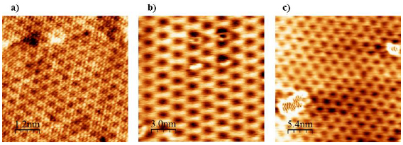
Figure V.28. STM images of SLG grown from C60 on: (a) Pt(1 1 1), (6 × 6)nm, 0.11 V, 2.3 nA. (b) Ir(1 1 1), (15 × 15)nm, 1.2 V, 2.6 pA and (c) Cu(1 1 1), (27 × 27 nm), −0.4 V, 2.7 pA. In every image different moiré superstructures are shown.
Download figure:
Standard image High-resolution imageThe same method works for other metals like Pt or Ir. Table V.1 shows the differences between the growths on the various substrates.
Table V.1. T and typical evaporation times needed to grow SLG from thermal decomposition of C60 for different substrates (at a sample-evaporator distance ~10 cm).
| Substrate | T sample during evaporation (°C) | Time to have SLG |
|---|---|---|
| Cu foil | 800 | 90' |
| Cu(1 1 1) | 900 | 30' |
| Pt(1 1 1) | 850 | 30' |
| Ir(1 1 1) | 900 | 30' |
There is still a lack of a precise atomic mechanism rationalizing the thermally-assisted on-surface decomposition of fullerenes on metals, whose foundations still remain unclear. The process needs the synergistic effect of surface T and availability of enhanced reactivity sites on the metal surface: such as atomic metal vacancies, kink/add surface metal atoms or metal surface steps. The combination of these factors favours the anchoring of the C60 molecules to the surface strongly enough to disrupt their stable geometrical arrangement (see figure V.29). A strong interaction of C60 with the sites with enhanced-reactivity could lead to an efficient weakening of the C–C bonds within the cage-like configuration contacting with the surface, in particular, of the C–C bridges participating in pentagon-rings of the C60 molecules, which store less energy than those connecting hexagon-rings. The process will start with the molecular cage rupture toward the on-surface disaggregation of the molecules into C atoms or other flatter C-based structures, free to diffuse on the metal surface by effect of the T.The epitaxial graphene growth will undergo by aggregation of the mentioned on-surface diffusing C atoms or C-based nanostructures (see figure V.29), which will lead to the formation of the most stable graphene domains on the metal substrates.
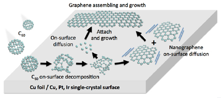
Figure V.29. Pictorial sketch corresponding to the thermal PVD decomposition of C60 on the mentioned Cu foils, and Cu, Pt and Ir single-crystal surfaces, as well as the coexisting subsequent processes leading to the growth of graphene.
Download figure:
Standard image High-resolution imageV.2. Graphene growth on semiconductors
Working conditions in CMOS fabs are extremely restrictive in particular regarding metal contamination [1718] Transfer technologies are being improved to provide a very clean environmentDirect growth on semiconductors would be the ideal alternative.
V.2.1. Graphene growth on Ge
It would be desirable to grow graphene on high quality single crystals. Graphene on SiC is of high quality and may satisfy some applications. However, these are limited to the use of SiC as a substrate. Other than on SiC, most of the high-quality isolated graphene has been grown on metal surfaces because of their high catalytic activity and limited C solubility. While as a single crystal is not widely used in the semiconductor industry, it is used as an alloy with Si (SiGe) in the sources and drain of advanced transistors and it could also be deposited selectively onto Si. With respect to its ability to be a good graphene substrate, Ge like Cu has an extremely low C solubility and it does not form a carbide, [930] thus potentially making it a good candidate for graphene growth. Ref. [931] took advantage of this and found CVD growth conditions for SLG. Additional work was performed on the growth of graphene using other techniques such as APCVD, [932] and MBE, [933] on Ge(1 1 0), Ge(1 0 0) and Ge(1 1 0)/Si(1 1 0) and Ge(1 0 0)/Si(1 0 0). Although Ge is more 'compatible' in Si device flows, there are still challenges: transfer and crystallinity. These could be overcome by developing growth selective techniques on isolated Ge/Si post transistor fabrication. Ref. [934, 935] reported the CVD growth of graphene on monocrystalline Ge(1 0 0) on Si(1 0 0), the preferred orientation of Si for CMOS technology. The growth took place between 900 and 930 °C with a ramp-up rate of 1–20 °C min−1 and CH4 flow in the (0.4–5 sccm) range. The optimal roughness of the substrate was achieved when the step growth was preceded by annealing at 750 °C–800 °C in pure H2 to reduce native oxides in situ [936, 937]. Ref. [934, 935] also grew SLG on Ge(1 0 0)/Si(1 0 0) under laminar conditions with a Aixtron VP508 horizontal CVD hot wall reactor. The SLG growth was perfromed at 890 °C–910 °C with a ramp-up rate ~1 –10 °C min−1 and a pressure ~850–990 mbar. CH4 at flow rate ~0.1–0.5 sccm was used in an Ar flow ~3 l min−1. The step growth was preceded by substrate annealing at 800 °C–850 °C in H2.
V.3. Graphene growth on insulators
V.3.1. High temperature CVD growth
The production of large area polycrystalline graphene and graphene single crystals has been demonstrated via chemical vapor deposition (CVD) on metal catalyst. Currently, the major drawback is the transference of the large area graphene film to the desired substrate for applications that normally induces contamination, wrinkles or even breakage of graphene. In this scenario, the game changing breakthrough would be the development of processes to deposit directly high quality graphene films and single crystals on arbitrary substrates avoiding the transference step and, if possible, at lower T than catalytic approaches. The first route involves the direct CVD synthesis on insulators or dielectrics at T > 1000 °C with examples of synthesis surpassing 1500 °C [943]. Along the high T, atmospheric pressure and CH4 as precursor diluted typically in Ar and/or H2 are the most common parameters. Synthesis of SLG and FLG films was on reported on Si3N4 [938, 939], sapphire (Al2O3) [940–943] and silicon oxides in different structures [944–946] with final Rs between 5 kΩ [944] and 800 Ω [945]. FLG grains were also deposited on h-BN flakes at 1000 °C in atmospheric pressure CVD [947] and on MgO nanocrystal powder by LP CVD at lower T between 325 and 875 °C [948]. Other substrates include SiC [611] and SrTiO3 [949] with µ ~1800 and 1050 cm2·V−1·s−1. Even though, the typical grain size is smaller (between 0.5 and 10 µm) and the amount of defects higher in comparison with the graphene synthesized with the catalytic approach, the final properties of the deposited graphene resemble transferred material grown on catalytic metals [945].
V.3.2. SiO2
SiO2 whether in bulk form as transparent quartz or fused silica or on thin films grown on Si wafers (SiO2/Si), are the most frequently used insulators to directly growth graphene. In the case of the transparent substrates, the typical features of these films include transparency from 80% to 95%, nearly maintaining the transmittance of the substrate itself in some cases, and tunable Rs depending on process parameters [950–954] with values ranging from 1 kΩ sq−1 [954] to few kΩ sq−1 [952]. Those transparent materials have demonstrated potential for a broad range of daily life applications as heating elements in smart windows, high performance defoggers with fast response (one minute) [951], anti-icing glasses or as mechanical strain or rupture sensors (demonstrated GF ~600 [955]), to name a few. The main limitation to transfer this knowledge to the industrial environment is the high growth T.
Given that Si based electronic technology is the established standard, it would be also extremely interesting to grow graphene on SiO2/Si wafers so as to integrate graphene in Si-based devices. Many approaches have been developed in this area, but the temperature required, typically over 1100 °C [944, 945, 951, 954, 956–958], poses some problems derived from the poor thermal stability of SiO2. Among them, desorption of SiOx from the exposed surface [956] and diffusion of carbon or silicon species from the interface) [951] are well known phenomena that play an undesirable role during synthesis, affecting the structure and quality of the deposited graphene. These effects are more pronounced in thin oxide layers (less than 90 nm) [951] that, in turn, are an important issue in CMOS technologies [959]. Confinement of the substrate was suggested to eliminate desorption [956]. Even so, the final µ ranged from 410 to 760 cm2·V−1·s−1much lower than catalytic CVD. In order to manage the stability issue, PECVD has been considered as an alternative approach to direct deposit graphene at lower T [962].
V.3.3. PE CVD on SiOx and Si/SiO2
PECVD enables catalyst free direct growth by the activation of molecules in gas phase and reduces the high T in conventional CVD or in attempts to use pyrolysis [938, 939, 941, 942, 944–948]. The most important drawback is the resulting small grain size.
PECVD has been reported on non-metallic substrates, resulting in films with small grain sizes -from 2 to 30 nm-, and amorphous carbon [816, 960, 961]. Ref. [774] reported an enlargement of grain size by a 'two-step' growth strategy in remote electron cyclotron resonance plasma assisted chemical vapor deposition, r-(ECR-CVD), figure V.30. The entire protocol is shown in figure V.31.

Figure V.30. Schematic illustration (left) and picture (right) of a r-(ECR-CVD) Plasma system. This consists of a gas delivery system with flow controllers, an ASTEX AX 2000 microwave power source with optic fiber coupling the power to the discharge plasma chamber with an ECR magnet surrounding it. The activated gases are transported by forced convection, with two electrodes attracting electrons and ions. The substrate is independently heated. A two stage pumping system generates the vacuum. Adapted from [816], © IOP Publishing Ltd.
Download figure:
Standard image High-resolution image
Figure V.31. 'Two step' synthesis protocol schematics.
Download figure:
Standard image High-resolution imageThe various parameters (time (t), T and partial pressures of C2H2 and H2, PC2H2 and PH2) were tuned 'in situ' in the nucleation (t1, T1, P1C2H2/P1H2) of high quality graphitic seeds and growth from the seeds edges (t2, T2, P2C2H2/P2H2) stages. A post-growth annealing is applied in UHV, improving the final properties of the film. The detailed procedure is usually as follows:
- Evacuation down to 10−5 mbar, introduction molecular H2 at a P1H2 = 10−2 mbar (typical flow of H2 = 55 sccm) and increase T up to T1 = 500 °C–700 °C in 40–60 min (t0, figure V.31) for stabilization. Subsequently, annealing the substrate for 5 min. In some cases is interesting to bias the substrate with a positive potential (0 V–50 V) if the auto polarization due to the plasma is not positive.
- Step 1 (NUCLEATION): Introduction of C2H2, at a P1C2H2 = 10−4 mbar, typical flow = 0.25:0.20 sccm and turn on the plasma (100 W) during 5 min (t1, figure V.31).
- Step 2 (GROWTH): Modify T2 in a range of 30 °C–100 °C or P2C2H2/P2H2 in the 0.1–0.9 · 10−4 mbar range (between 10%–20%), maintaining it for few hours (t2, figure V.31), until the substrate is completely covered. As a general rule, P2C2H2 is modified, due to its minimal relevance in the final pressure.
- Turn the plasma and bias off and cut the flow of precursor (P2C2H2), cooling down in hydrogen atmosphere (P2H2) during 40 min (t3, figure V.31) preventing oxidation. Post growth annealing in UHV at 650 °C, to desorb some chemical species attached to grain boundaries and to improve the coalescence among the grains.
V.3.4. PECVD on quartz substrates
Following the above protocol graphene was deposited on quartz as depicted in figure V.32. AFM images of lateral force contrast are shown in figures V.32(a)–(c). Raman analysis indicates the formation of predominantly highly defective SLG at 650 °C, figure V.32(d).
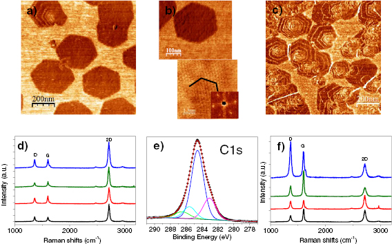
Figure V.32. Graphene on quartz at H2/C2H2 = 55/0.25:0.20 (sccm), PT = 5.4 × 10⁻² mbar, P = 100 W for 5 min nucleation time, 9 h growth. AFM lateral force image of the sample grown at (a) T = 650 °C and, (b) high magnification lateral force image of a single flake from sample and below the corresponding atomic lattice periodicity of the flake along with the Fast-Fourier transform in the inset of the periodicity image in (a)–(c) AFM lateral force image of the sample grown at T = 700°. (d) and (f) Individual Raman spectra acquired at grain positions, for samples in (a) and (c), respectively. (e) High resolution XPS C1s core level spectrum (black dots) of the sample grown at 650 °C. The C-sp2 graphitic component (blue, 284.6 eV), C–H (green, 285.6 eV) likely from H-terminated edges, and C–O (cyan, 286.5 eV) species. The component at (magenta, 283 eV) can be ascribed to remainders of the growth process (e.g. C2H4Si at 282.5 eV) or to the interaction with substrate (e.g. SiC C(1s) is 282.5–283.5 eV). Adapted from [774], © IOP Publishing Ltd.
Download figure:
Standard image High-resolution imageFigure V.33 presents an AFM characterization of continuous film, confirmed by four point probe measurements, with a RS ~ 3.4 kΩ·sq−1. The coalescence of graphene grains follows two different trends (figures V.33(a) and (b)). Hexagonal graphene domains of similar orientation often generate a smooth lateral merging, presenting boundaries without linear defects (figure V.33(b), black arrows) [611, 931, 962–965]. On the other hand, rough lateral merging also takes place at many points, where linear defects occur (figure V.33(d), pink line). On these defects, carbon species accumulate as in vertical graphene deposition [966] that indicates that the process is not completely self-limiting. From UV–vis-NIR spectrophotometry transmittance (figure V.33(c)), it is also clear that there is an influence of this accumulation (values ~95%).

Figure V.33. Characterization of continuous film T = 650 °C, H2/C2H2 = 55/0.25:0.20 (sccm), PT = 5.4 × 10⁻² mbar: P = 100 W. (a) and (b) AFM topographic images of graphene deposition on quartz for 5 min nucleation time and 10 h growth. (c) Transmittance spectra before (95%) and after (92%) post-growth annealing. (d) Height profiles taken along the corresponding lines in (b) (film thickness, cyan).
Download figure:
Standard image High-resolution imageAfter growth, the sample can be annealed in UHV to improve the final properties. Ref. [774] increased T stepwise up to 600 °C. The height and density of the linear defects is lower after annealing. RS decreased from ~3.4 kΩ·sq−1 to ~900 Ω·sq−1, with transmittance > 92%. The protocol is scalable it is likely accelerated by changing plasma power and pressure.
The r-(ECR-CVD) mode activated by microwave (MW) source provides higher efficiency in the dissociation of gases than other plasma and it is especially efficient in the dissociation of H2. It is one order of magnitude more efficient than other DC (continuous polarization) and RF (radiofrequency) plasma sources. Along with the activated species and neutral radicals, ions and electrons coexist, being mostly the highly energetic ions a potential cause of etching of films. From a geometric point of view, a minimum distance between the plasma zone and the substrate (20 cm) should be respected ('remote plasma activation'). Moreover, the inhomogeneous plasma activation (plasma ball) results in different deposition rates on different sites. For this reason, to make de process reproducible the position of the sample in the holder is critical and must be respected. Apart from geometric considerations, one parameter that can minimize the presence of remaining ions reaching the sample is the positive bias of the substrate [967–969]. The activation of the substrate is also minimized preventing high nucleation density. The last fundamental plasma parameter is the power; the higher the power, the grater is the gas activation. However, as this protocol is a competitive process between etching and growth, assessing the role of power is not straightforward. The increase of power itself does not reflect a proportional increase of all species.
A T increase keeping the other parameters fixed, results in an increase of the reaction rate but at the expense of an enhanced nucleation density due to the present dangling bonds in freshly activated oxide surfaces. As a minimum T > 400 °C is needed for graphitization, the key is to favor the reaction at the graphene edge instead of reaction with substrate by carefully playing with the local saturation of carbon. In figure V.32, a deviation in T from the established recipe affects the nucleation density, growth rate, microstructure and N. Figure V.32(a) shows single layer grains at 650 °C. At 700 °C, figure V.32(c) more flakes of few layers are predominant. Side chemical and topological effects take place, as covalent bonding with substrate or etching, hindering the desired van der Waals interaction. Formation of carbide phases or volatilization of oxide species (CO, H2O, OH, SiO...) can be produced. There are interdependence between pressure and T, as the unbalanced pressure has similar effects, as observed in figure V.34 (variation of 20% of gas flow). If hydrocarbon flow is below the critical value at a given T, there is no deposition in the nucleation step. If it is over, the deposited nuclei suffer from amorphization. In the second step, a similar effect occurs with (T2) or partial pressures relation, P2(C2H2)/(P2H2), resulting in secondary nucleation or etching of the deposited material. In figures V.34(a) and (c) a deposition of submonolayer graphene can be seen in topography and friction images. In figures V.34(b)–(d) more few layer flakes are deposited increasing pressure.
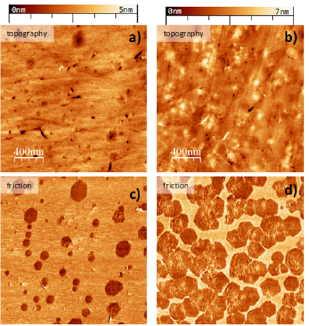
Figure V.34. Graphene on quartz T = 650 °C, PT = 5.4 × 10⁻² mbar: P = 100 W. t1 = 5 min. t2 = 690 min. Topographic (top row) and corresponding lateral force (bottom row) AFM images of samples grown at increasing pressure from (a) and (c) H2/C2H2 = 55 0.25:0.20 (sccm) to (b) and (d) H2/C2H2 = 55/0.30:0.25 (sccm). The increase in the number of FLG with increasing pressure is seen.
Download figure:
Standard image High-resolution imageThe precursors and atomic hydrogen, also play a critical role. An appropriate H/CxHy ratio in the atmosphere is necessary to grow crystalline material [970]. There is a competition between growth from CxHy radicals and etching of amorphous deposits by atomic H [971, 972]. The etching rate depends on T and N.
Ref. [774] found that C2H2 is a suitable precursor for low T, and no relevant differences between the films deposited with CH4 and C2H2 diluted in hydrogen, once the appropriate H/CxHy relation and T) settings are selected. For C2H2 the activation is much higher due to combination of plasma and thermal activation (that does not happen with CH4) [973]. This enhances the reaction rate because the plasma environment is full of activated carbon dimmers, postulated as the main precursor, or at least the main intermediate product, in the case of the synthesis of graphene, due to their higher mobility [974, 975].
Ref. [774] used fused silica at high T up to 700 °C. However, some kind of modification was detected in the surface and changed to quartz.
Dangling bonds in freshly activated surfaces (oxides or insulators) promote strong chemical interaction between the surface and gases. To overcome this limitation the two step process was developed Ref. [774] where the edge growth from seeds is highly favored over the nucleation on substrate. Even so, some limitations continue as the process is slow and not completely self-limiting as can be seen in figure V.34(d) where several layers conforming a multilayer deposit (rose petals shape) is apparent. The origin of this multilayer deposits is the slight reduction of the quartz surface.
The reduction process of the quartz surface has been computationally simulated by modelling the quartz [1 1 − 2 0] facet (x-cut), assessing the activation energies for the most probable reaction paths within the CI-NEB approach [916, 917] (see figure V.35(a)). Protonation of surface oxygen with atomic hydrogen from plasma and subsequent water vapour release are highly probable in this surface at Si synthesis T[774]. The passivation of the silicon enriched surface with hydrogen prior growth is also favoured because the Si detachment is more energy demanding. Simultaneously to the different steps along the reduction of the quartz surface (figure V.35(a)), plasma products, acting as reaction precursors toward the formation of graphene, start to adsorb on the surface, which will lead to their decomposition and dehydrogenation, favouring the nucleation at specific enhanced-reactivity sites, depending on the surface reduction stage (see figure V.35(b)). Graphene nanopatches will grow from the incorporation of dehydrogenated carbon atoms, as well as from nucleation centers catalysed by the surface. The coexistence of these processes with the plasma atomic hydrogen maintains the H-passivation and de-passivation (by surface-assisted H2 formation) equilibrium in the surface promoting the plasma precursors into graphene.
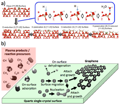
Figure V.35. (a) Side view of the different DFT-computed steps along the reduction process of the [1 1 − 2 0] quartz surface (adapted from [774], © IOP Publishing Ltd): starting from the clean hydroxylated surface [976] across subsequent protonation barrierless steps and detachment of H2O molecules (see inset), which lead to slight surface reconstructions, and H-passivation of the surface. (b) sketch corresponding to the coexisting processes leading to the growth of graphene on a quartz single-crystal surface from the different plasma products by PECVD: adsorption, decomposition and dehydrogenation of the reaction precursors, toward graphene nucleation and formation.
Download figure:
Standard image High-resolution imageV.3.5. PECVD on Si/SiO2
PECVDis as an alternative approach to directly deposit graphene at low T. Several studies were reported on the grown of graphene by PECVD over Si/SiO2 with thick (250–300 nm) and medium oxide layers [977, 978], resulting in BLG or FLG [979, 980]. Ref. [981] addressed the direct growth of graphene on Siwafers with ultrathin native oxide by r-(ECR-CVD) using the two-step protocol discussed throughout this section to separately control nucleation and growth stages [977, 774], enabling tuning of grain size and thickness.
Figure V.36 is one example of graphene nuclei obtained at 550 °C following the two step protocol using two C2H2 flows. The increase of C2H2 flow in the nucleation step from 0.8 to 0.9 promotes a moderately increase of the nucleation density for a particular nucleation time (~30 nuclei µm−2). Also, the increase of C2H2 flow from 0.7 to 0.8 sccm increases the grain size during a given growth time. The height profiles in figures V.36(a) and (b) evidenced that, despite the different graphene nuclei sizes, for both experimental conditions, the thickness of the nuclei remained below 1 nm, resembling the features of SLG on quartz [774]. During the synthesis, the SiOx surface is not affected in terms of surface roughness.

Figure V.36. AFM topographic images of graphene nuclei and corresponding profiles at 550 °C, PT = 5.4 × 10⁻² mbar, P = 200 W, H2 = 50 sccm, t1 = 5 min, t2 = 150 min. (a) C2H2 flow: 0.9 sccm in the nucleation and 0.8 sccm in the growth step. (b) C2H2 flow: 0.8 sccm in the nucleation and 0.7 sccm in the growth step. Adapted from [981], with permission of The Royal Society of Chemistry.
Download figure:
Standard image High-resolution imageAfter nucleation, the enlargement of the nuclei in figure V.37(a) follows to complete the deposition of a continuous film. Figure V.37(a) shows the submonolayer coverage of the substrate. Longer t2 (seven hours) enables the creation of graphene domains up to 300 nm in lateral size. Flake thickness, as shown in figure V.37(b), corresponds typically to SLG. The coalescence of the domains occurred without vertical growth at the grain boundaries as seen in figure V.37(c) but the surface of the film is not completely flat. Inhomogeneous stitching between grains is apparent, along with lack of continuity in some others (darker contrast). Figure V.37(d) presents the corresponding Raman spectra before and after annealing. The Raman spectrum from submonolayer coverage shows the characteristic graphene peaks. I(2D)/I(G)~1 and 2 and FWHM(2D) 38 cm−1. The high I(D)/I(G)~ 1 is due to the high density of grain boundaries and defects. Along with grain boundaries, another source of defects could arise from the hydrogen enriched atmosphere during deposition, which functionalizes the graphene grains and boundaries, inducing some re-hybridization in the corresponding carbon atoms [982]. The Raman spectrum in black from the continuous film in figure V.37(c) shows similar results. The continuity of the film in figure V.37(c) was also confirmed by four point probe measurements (Rs~15 kΩ·sq−1) This high value can be related to these aspects mentioned: incomplete stitching in some grain boundaries due to randomly oriented grains and functionalization [972]. Thisdecreased to 8 kΩ·sq−1 after annealing at 650 °C in vacuum at 10−6 mbar, lower than reported for low T procedures [977]. After annealing, I(D)/I(G)decreases from ~1.1 to 0.9. This could be related to H desorption from the film inducing sp2 hybridization in the carbon atoms [774]. The decrease of Rsafter annealing could be also related to the same reason: H desorption from grains and boundaries and conversion of carbon hybridization [774, 982, 983].
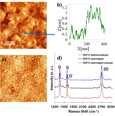
Figure V.37. (a) AFM topographic image of graphene nuclei at 550 °C, H2/2H2 = 50/0.9:0.8 (sccm), PT = 5.4 × 10⁻² mbar: P = 200 W, t1 = 5 min t2 = 7 h. Vertical scale: 0–5 nm (b) Corresponding profile from a graphene flake in (a). (c) Continuous film, t2 = 10 h and same conditions than (a). Vertical scale: 0–5 nm. (d) Corresponding Raman spectrum of sample (a) (blue) and (c) before (black) and after annealing (red).
Download figure:
Standard image High-resolution imageV.3.6. PECVD of vertical structures
PECVD can be used to synthesize graphene on insulators. In Ref. [854–856] a cold wall chamber was pumped by a turbo pump and an RF plasma power of up to 1000 W is applied on top of the chamber, through a matching network. H2 and CH4 are used as precursors (figure V.38(a)). Different growth conditions were investigated and the highest film uniformity was achieved by using a 1000 W RF plasma, a T = 750 °C and a growth time of 20 s. Figure V.38(b) shows an AFM image of the grown film directly on Si/SiO2, highlighting a film roughness of 0.624 nm. The film thickness was 3.33 nm (figure V.38(c)), indicating MLG.
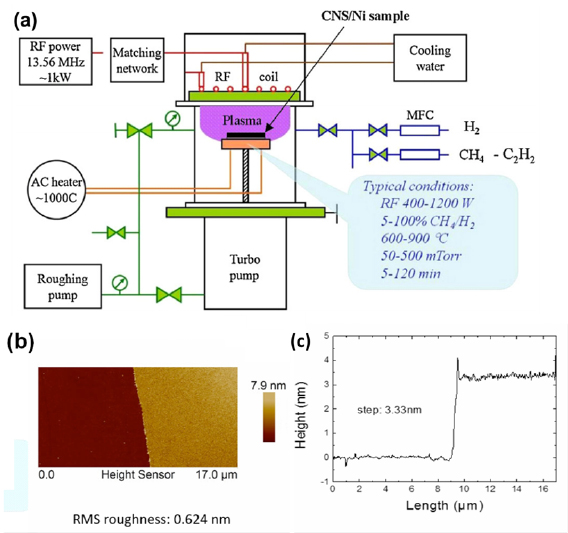
Figure V.38. (a) Schematic PECVD system used to grow graphene on Si/SiO2. Figure reproduced from [856], with permission from Elsevier. (b) AFM image of the grown graphene film (c) Height profile.
Download figure:
Standard image High-resolution imageV.3.7. CVD graphene by sacrificial metal layers on Si/SiO2
By replacing Cu foil with a thin sacrificial metallic film one may arrive at an alternative route for graphene deposition on dielectrics. The proposed approach is based on the fact that in the CVD process, graphene grows on the Cu-substrate interface provided that carbon precursors have access to it [802, 984]. Thus, by removing graphene from the Cu surface by RIE and then removing the Cu catalyst by wet etching, one can obtain graphene on a silica substrate [802, 984].
Ref. [984] used up to 300 nm thick thermally evaporated sacrificial layers of 99.999% pure Cu on silica or Si/ SiO2. Cu evaporation does not require UHV, although the higher vacuum reduces the oxidation of the deposited Cu film. Ref. [984] indicated that a vacuum level ~10−5 Bar is sufficient. Since the surface of the deposited Cu layer rapidly oxidizes in an ambient atmosphere [985], it is advisable to start the CVD process soon after evaporation to minimize the amount of Cu oxide. Otherwise, Cu oxide can be removed by treatment of the deposited layer in acetic acid [985, 986]. Ref. [984] placed the substrate into the CVD chamber immediately after Cu deposition and pumped down the chamber for an hour. While pumping, 5 sccm H2 is admitted to remove moist and air remains from the chamber. Thereafter, the chamber is heated up to 700 °C in H2 (5 sccm, 0.5 mBar, 20 °C min−1). At 700 °C the CVD chamber is vacuumed and CH4:H2 (1:1) gas mix injected (8 mBar, static atmosphere). T is risen (10 °C min−1) up to 950 °C and kept for 5 min and then the chamber is cooled down to 700 °C in one hour. At 700 °C the CH4–H2 gas mix is replaced with H2 (10 mBar) and the chamber is cooled down to RT overnight (see also [984, 987]).
Surface melting is a key process that governs the deposition of graphene [984]. Although the melting T of bulk Cu is 1084 °C, the melting of low dimensional systems takes place in a much lower range [988]. Therefore, although the hydrocarbon catalysis starts ~800 °C–900 °C [989, 990], in Ref. [984], CH4 was injected into the chamber at 700 °C. At this T, catalytic decomposition of CH4involves mobile atoms of molten Cu. Since the carbon solubility in Cu is very low (<10 ppm at 950 °C) [790], the migration of the carbon atoms bound to Cu atoms is mainly restricted to the surface [802, 881, 882]. When a few hundred nm thick Cu film melts, melting of each Cu grain results in well-defined grain boundaries [802]. Highly mobile Cu atoms carry carbon atoms along the molten grain boundaries allowing them to penetrate into the Cu film and arrive at the substrate surface [802, 984]. This effect eventually results in graphene synthesis on substrate-Cu interface. After reaching the maximum T ~ 950 °C the reactor cools down very slowly, i.e. the carbon precursor (CH4–H2 mixture) is available for graphene synthesis at the surface of the molten Cu grains until the Cu solidifies at 700 °C.
The Cu film thickness is an important parameter [984]. When the thickness of an original Cu film is <100 nm the molten Cu film recedes forming mainly round droplets of submicron radii covered by graphene, with no graphene between those Cu droplets. When the thickness is ~300 nm the Cu film remains solid after the process, resulting in a grainy but continuous graphene film to the Cu-substrate interface [984].
The topmost layer of graphene can be removed from Cu by oxygen plasma (20 sccm/100 W/1 min), while the remaining Cu protects the graphene layer at the Cu-substrate interface. The remaining Cu is etched by ferric chloride solution. If the topmost graphene is not removed, it will usually stay on the substrate surface as small, arbitrary ribbons and fragments.
Raman characterization in figures V.39(c) and (d) shows a small D-peak and the absence of amorphous carbon [991]. The SEM image in figure V.39(b) indicates that the material is grainy and consist of µm and sub µm flakes. Ref. [802] reported a rather poor µ ~300 cm2 V−1 s−1. However, the linear and nonlinear optical properties of directly deposited graphene are somewhat comparable to graphene grown on Cu foil [992].
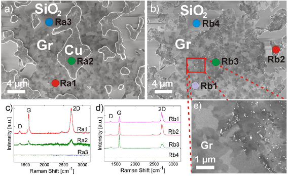
Figure V.39. SEM images of sample with (a) and without (b) and (c) Cu catalyst remains after CVD. Raman spectra with (c) and without (d) Cu catalyst. (e) High resolution SEM image from border area where Cu remains are removed. Adapted from [984], with permission from Elsevier.
Download figure:
Standard image High-resolution imageOne major part of the process is that of the substrate surface. Similarly to controlling the water droplet behaviour by modifying the surface wettability [993], surface modifications can be used to control molten Cu [987]. In figures V.40(a)–(c) one can observe a grating structure that has been under the Cu film during CVD. The continuous Cu film has first molten and receded in between grating lines. Under those Cu lines, graphene lines are located. When the width of the grating lines is sub-µm, the lines are no more discrete but sometimes merge together [987].

Figure V.40. (a)–(c) SEM images of sample before CVD, after CVD and after Cu removal in FeCl3. (d) and (e) Raman mapping reveals graphene on the grating. (f) Raman spectrum of the grating area is comparable to that grown outside. Adapted from [987], with permission from Elsevier.
Download figure:
Standard image High-resolution imageDeposition on thin Cu film does not offer an ideal route for graphene synthesis. An important drawback is the very high, 900 –1000 °C deposition T. This makes graphene deposition impossible on some substrates because (i) substrate melting (e.g. polymer substrates), (ii) recrystallization of a thin film (e.g. amorphous titanium dioxide) or (iii) thin film-substrate thermal expansion mismatch, which may cause thin film material to crack out from the substrate surface. Moreover, high synthesis T may start a chemical reaction between the metal and the substrate (e.g. Si may react with Cu or Ni).
Another approach demonstrated that even at near RT (60 –160 °C) graphene can be deposited from graphite powder by using Ni as catalyst [814]. A thick Ni polycrystalline film was firstly deposited over the substrates (SiO2/Si, glass and PMMA). Then the stack heated at low T. Ref. [814] suggested that carbon diffuses through the Ni film boundaries to the interface. At 160 °C continuous graphene films of reasonable quality (~667 cm2·V−1·s−1) was deposited on SiO2, however N was barely controlled. At lower T (from 60 °C to 160 °C) the deposition of continuous films is avoided being the coverage from 60% to 98% and the grain size and quality of the deposits deteriorate. At 60 °C on glass and PMMA the Raman signal shows the deposition of highly deteriorate graphene layers with nanometric grain size.
Another route is the use of alloys as catalysts, an approach well-known in heterogeneous catalysis to tune the reactivity and selectivity of precursor molecules. Low T (~450 °C) SLG (74%) was demonstrated via the catalysts alloying (sputter deposited polycrystalline Ni films covered with evaporated Au. The initial Au top-layer dissolves into the Ni upon annealing) [878]. The nucleation density is reduced and the graphene domains exhibit lateral dimensions >15 µm. The main limitation is the lack of control in the deposition of monolayer films without multilayer areas [877].
Pd–Coas a catalyst was introduced to realize low T graphene growth on glass substrate by using remote RF PECVD [877]. FLG films were formed with high transmittance ~88.8% and Rs~66 kΩ·sq−1 at T as low as 400 °C, in contrast with Ni catalyst in which no graphitic layer was formed. High decomposition rate of hydrocarbon gases and formation of nanosize aggregates enhances the carbon incorporation into PdCo alloys and as a consequence, a graphene layer is formed at low T. The graphene may be further improved by optimizing Co composition and CVD conditions.
V.3.8. Conversion of amorphous carbon and other carbon sources on sacrificial layers
For this purpose, one can employ liquid and solid carbon precursors for graphene synthesis [814, 847, 994–997]. Regarding the substrate, due to higher carbon solubility and lower reaction T, Ni can be considered a more aggressive catalyst in comparison to Cu. Its use may be advantageous when solid carbon precursors are chosen. Ni-catalysis is activated at a few hundred degrees lower T than Cu [182, 802, 814, 984, 994–997] and may open pathway for direct deposition on bendable substrates [881, 882, 995, 998]. The drawback of Ni is the high C solubility (~0.6 w% Ni at 1326 °C [999] that makes difficult to control the deposition process.
Typically, the amount of carbon precursors determines number of carbon atoms available for the catalysis, while the temporal evolution of the process T governs N [1000]. The cooling rate is important since it defines either the dissolved C will stay inside Ni or be squeezed on a Ni surface forming SLG or FLG films [1000], while the amount C dissolved in the Ni is determined by catalyst amount. Ref. [1001] minimized the thickness of Ni to decrease the amount of dissolved carbon because precise T control of the bulky hot wall CVD of was hardly possible. Ref. [1001] used 10 nm thick Ni film on a silica substrate as a catalyst and the carbon precursor was nLOF photoresist (AZ nLOF 2070, negative tone resist diluted with AZ EBR 70 thinner). The pyrolysis T of the photoresist film in the CVD chamber varied from 600 to 900 °C and resulted pyrolyzed photoresist film (PPF) with and without Ni [1001]. Since during the CVD process some part of the resist layer is expected to evaporate, the Ni film was deposited under the nLOF layer. Thus the Ni layer did not prevent the evaporation from the resist layer.
Similarly to Cu, Ni will also melt and recede during CVD. Since the thickness of the original Ni film was only 10 nm the particle size is in sub-µm range. Figures V.41(a) and (b) show the appearance of the Ni particles on PPF pyrolyzed in 800 °C. In Ref. [1001] the T dependence to the PPF graphitization was observed by Raman spectroscopy. Most significant changes in the structure of the PPF with Ni took place For T = 800 °C or above (see figures V.41(c) and (d)) [1001]. A 2D peak appeared at 2705 cm−1. The D and G peaks became narrower, indicating higher degree of crystallization in to comparison to PPF pyrolyzed in 700 °C and lower T or without Ni catalyst.
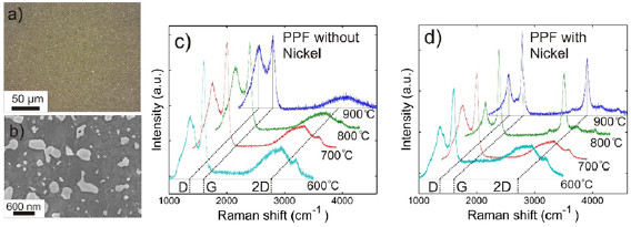
Figure V.41. (a) optical microscope and (b) SEM image of PPF with Ni particles fabricated at 800 °C. SEM reveals non-uniform size and shape of Ni particles (bright particles). Raman spectra shows the evolution of the carbon film as a function of temperature (c) without and (d) with Ni in the process. Adapted from [1001].
Download figure:
Standard image High-resolution imageOne approach to control the growth process and improve the quality of graphene grown by catalytic transformation of solid carbon sources was the introduction of a carbon diffusion barrier (Al2O3) between Ni catalyst and carbon layer [817]. At thin Al2O3 barrier enabled the growth of SLG at 600 °C, with domain size >50 µm and quality that equals the CVD grown films at similar T.
The direct formation of graphene on various dielectric surfaces via a single-step rapid thermal processing (RTP) of substrates coated with amorphous carbon and nickel (Ni) thin films has been reported [1002]. Here, high-quality graphene was obtained uniformly on the whole surface of wafers with a controlled N. SLGshoewd a low Rs and a high optical transmittance in the visible.
V.4. Brief comparison of all methods
There is a wealth of methods to grow graphene on a variety of substrates. Some are more suitable to grow on catalytic substrates while others are better for insulators. Most of them exploit a variety of precursors. Table V.2 summarizes methods, substrates, precursors and optimal growth conditions.
Table V.2. Methods, substrates, precursors and optimal growth conditions.
| Method | Substrate | Precursor | Temperature | Pressure | Lateral grain size |
|---|---|---|---|---|---|
| CVD | • Cu Foil | CH4, C3H8 | 1000 °C < T < 1084 °C | 0.5 mbar–1 bar | 10 µm |
| • Partially oxidized Cu foil enclosed | Few mm-cm | ||||
| CVD | Cu foil | C2H4 | 850 °C | 2 mbar | 1 µm |
| CVD | Ir(1 1 1)/YSZ/Si(1 1 1) | C2H4 | 850 °C | 1 · 10−8—2 · 10−7 mbar | Up to a few mm |
| CVD | Ge(1 1 0) on Si(1 1 0) | CH4 | 900 °C–930 °C | 850–990 mbar | <1 µm |
| CVD | Ni Foam | CH4 | 1000 °C | 50 mbar | Depends on metal foam structure |
| CVD | Cu Foam | CH4 | 1000 °C | 400 mbar | Depends on metal foam structure |
| CVD | Cu film on Silica wafer | CH4 | 950 °C | 8 mbar | <1 µm |
| PT-CVD | Cu | CH4 | 950 °C | 7–20 mbar | 1 µm |
| MBE | Au (1 1 1) | Glassy carbon filament | 550 °C | UHV | Tens of nm |
| PVD | Cu (1 1 1), Pt(1 1 1), Rh(1 1 1) single crystal or polycrystalline | C60 | 800 °C–900 °C | UHV | Tens of nm |
| PECVD | Glass or quartz | C2H2 | 600 °C–720 °C | 0.1–0.9 · 10−4 mbar | 500 nm |
VI. Graphene transfer, placement and decoupling from substrate
VI.1. Wet transfer
Many advances have been reported on the transfer of nanolayered materials such as graphene since the isolation of graphene on silicon dioxide and the growth of graphene on metal substrates [759, 765, 1003, 1004]. In 2007, Gölzhäuser et al were first to disclose a method to transfer nanolayers. Patents for this method were issued in 2013 and 2017 (Gölzhäuser; Armin, Nottbohm; Christoph, and Beyer; Andre, US Patent No. 8,377,243 B2 (19 February 2013), A. Gölzhäuser, C.T. Nottbohm, and A. Beyer, European Patent No. EP2144711B1 (31 May 2017)); this process is a wet transfer procedure very similar to the one published in the papers above. The nanolayer can be a single layer (SLG), bilayer (BLG) or multilayer (MLG) graphene but this aspect is not substantial for the purpose of the description of the transfer process. GRMs are covered with a polymeric layer that acts as surface protection as well as a carrier after the metallic substrate is removed by a chemical etchant. The polymeric layer, PMMA, with a thickness of several hundred nm, is used to coat the surface of GRM. One of the advantages of this process is that the polymeric layer conforms with the GRM surface without macroscopic damage. The resulting polymer/GRM/substrate structure is then dipped into a liquid etchant to dissolve the substrate or, alternatively, detached from the substrate. The latter can be achieved by electrochemical methods. After the substrate is removed/etched away or 'detached' an optically visible, several hundred nm thick polymer, with the GRM is left floating on the etchant surface. This 'hybrid layer' is then transferred onto a second desired substrate, typically a dielectric surface. Finally, the thick polymeric layer is dissolved or removed and the GRM remains on the target substrate.
VI.1.1. Etching of a metallic substrate
VI.1.1.1. Cu foil substrate
The wet transfer of CVD graphene on metals like Cu and Ni or its alloys by etching the metal is now broadly used [759, 764, 1003, 1004].
Once the graphene is grown on a large Cu metal substrate (foil) by CVD, the desired sample size is cut and transferred onto a 125 µm-thick PET foil, which acts as a mechanical support. Then a A4-950K poly-methyl methacrylate (PMMA) resist is spin coated on the GRM/Cu/PET stack at 4000 rpm for 40 s to achieve the desired thickness, up to ~400 nm, after which the PET support is removed. Since graphene grows on both sides of the Cu foil, that on the uncoated by PMMA has to be removed to prevent it from being combined with graphene under the PMMA. This graphene can be removed from the Cu surface using a reactive ion etch (RIE) process, typically using O2plasma at 20 W for 20 s and at 200 mTorr. The PMMA/graphene/Cu stack is then immersed/placed on the surface of a metal etching solution such as ammonium persulfate (APS), ~2.0 g in 150 ml of DI H2O, to etch Cu as shown in figure VI.1 and enable transfer of graphene onto a dielectric substrate. After Cu is dissolved, the remaining PMMA/graphene stack is lifted with the desired substrate (PET, SiO2/Si, or other) substrate and transferred to a container with DI H2O for washing. The procedure is repeated a few times to ensure that all of the etching solution is removed. After washing, the PMMA/graphene stack is removed from the water bath and left to dry. There are many implementations of this process and thus a lot of room for improvement as the processes are transferred to a pilot line or production environments. The PMMA/graphene/target substrate is then first transferred in a beaker with acetone for PMMA removal for 1 h, second to a beaker with isopropyl alcohol for 5 min and then dried with nitrogen, leaving the GRM on the target substrate.

Figure VI.1. Transfer of SLG from a Cu substrate to a dielectric surface. The top-right and bottom-left insets are the optical micrographs of SLG transferred on SiO2/Si with 'bad' and 'good' transfer, respectively. The bottom-right is a photograph of a 4.5 × 4.5 cm2 SLG on quartz substrate. Adapted from [1005], copyright American Chemical Society.
Download figure:
Standard image High-resolution imageVI.1.1.2. Au coated mica substrate
The transfer of a CNM grown on a Au coated mica substrate follows a slightly different path and can be applied also to the transfer to many target substrate [75, 76, 78, 1006]. The procedure is as follows: PMMA (950 K, AR-P 671.04, Allresist) is spincoated at 4000 rpm for 30 s, followed by a soft bake at 90 °C for 5 min. Optionally, a double layer of PMMA can be applied: (i) a first layer (50 K, AR-P 631.09, Allresist) is spun to a thickness of 130 nm at 2000 rpm for 30 s and baked on a hotplate at 90 °C for 5 min; (ii) a second layer of PMMA (950 K, AR-P 671.04, Allresist) has a higher molecular weight to provide mechanical stability. The latter is spun to a nominal thickness of 310 nm at 4000 rpm for 30 s and also baked at 90 °C for 5 min. The advantage of the additional PMMA layer with '50 K' is that it can be removed more cleanly than PMMA with a higher molecular weight in direct contact with the GRM. After the formation of the PMMA transfer medium, the edges of the sample are cut in order to ease the release of the PMMA/GRM from the mica substrate. Then, the sample floats on the liquid level of I2/KI etching bath (I2:KI:H2O with ratio of 1 g:2 g:10 ml) for ~10 min. Au is slightly etched from its lateral interface The separation of polymer/GRM/Au from mica is attained by dipping into water. To remove the Au layer, PMMA/GRM/Au floats on the liquid level of I2/KI etching bath for ~20 min. After wards the Au layer is completely removed, the polymer/GRM is transferred to a fresh water bath for rinsing. The hybrid transfer layer can be taken out of solution and placed onto a target substrate following the same protocols used to rinse it as detailed in the previous paragraph.
If the new host substrate is not solid and the GRM is to be free-standing on a grid-like substrate, removal of PMMA can be done by critical point drying [78, 1009] (CPD-) that avoiding the damaging effects of surface tension. The mounted sample is immersed into acetone. After 60 min, the chamber is cooled with liquid CO2 and then liquid CO2 is introduced into the avoiding turbulence. Liquid CO2 substitutes acetone according to a predefined time (15 or 20 min). Finally the dryer heats and pressurizes CO2 to its critical point, and gas CO2 bleeds off to leave nanolayer dry. A scheme of the procedure is shown in figure VI.2.
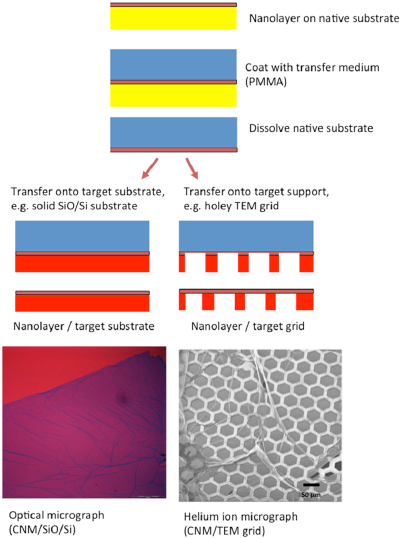
Figure VI.2. Top: Schematic of GRM transfer using polymeric media. Bottom, left: Optical micrograph of CNM transferred onto SiO2/Si showing interference contrast; bottom right: HIM of CNM transferred onto a metal grid without critical point drying. Ruptures and faults, as well as large intact areas of the freestanding nanolayer are visible. Adapted from [75, 1009].
Download figure:
Standard image High-resolution imageA HIM [1007] image of a CNM, placed onto a Cu grid with hexagonal pores of 40 µm, after removing PMMA without CPD, is show in figure VI.2. Note the appearance of wrinkles. The effect of critical point drying can be seen in figure VI.3(a) that shows a flat CNM on a grid with 40 µm openings. Figure VI.4(b) shows a very large free-standing CNM transferred onto a hexagonal grid with openings of ~0.5 mm [1007]. In both images, no folds and wrinkles are visible.
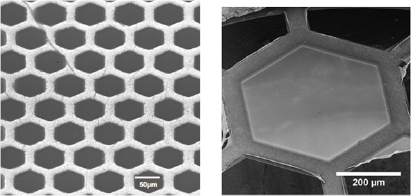
Figure VI.3. HIM image of large freestanding CNMs transferred onto hexagonal TEM grids. (left) The size of each hexagon is 50 µm and the grid is uniformly covered by the CNM.Scale bar is 50 µm. Right) The size of the hexagon is 500 µm and it is completely covered by CNM, no wrinkles or folds seen. Scale bar is 200 µm. Adapted from [1007].
Download figure:
Standard image High-resolution imageAn additional option of removing the PMMA is the inverted floating method (IFM) [1008]. Therein, only the PMMA covered side of the sample is in contact with acetone. Large graphene membranes were reported, covering circular holes in SiO2 substrates. This approach is most effective in circular support structures and it requires full coverage of the substrate openings. In contrast to IFM, CPD avoids surface tension related forces on the membrane. Therefore, if available, CPD seems to be a better choice for removing the PMMA layer.
Ref. [1009] systematically studied the effect of annealing of transferred graphene by PMMA by FTIR and XPS in oxidative environments (CO2, O2 and NO2) and found it more effective than in reducing ambients, such as forming gas or vacuum [1010]. More specifically, they found that annealing in an atmosphere of CO2 at 500 °C in a few minutes is very effective in removing PMMA (mainly carbon) without damage to the graphene. Atomic level cleaning of PMMA was also performed using radiolized water at high T. The cleaning process was studied by [1011]. The radiolized water was obtained via interaction of the electron beam in the TEM with water at high T. In this process of radiolysis, as the electron beam interacts with water and the graphene surface forms atomic hydrogen and hydroxyl radicals at high T. This process was reported at the submicron scale and will have to be demonstrated at much higher scales before considering it as a viable practical process, although it is contributing to the basic understanding of graphene surface cleaning.
VI.1.2. Electrochemical delamination
The use of PMMA as a carrier layer followed by chemical etching of the metal substrate is an effective way of graphene transfer. This process, however, can be time consuming and the whole metal substrate is etched away. The latter makes the process costly and environmentally unfriendly. It would be desirable to use a process whereby the graphene film is removed from the substrate without significant metal loss and without damaging the overlying graphene layer. Electrochemical delamination was introduced to accomplish this task. Ref. [779] reported this processes for graphene transfer from Cu substrates and in Ref. [108] for the delamination of graphene from Pt. This technique is nondestructive not only to graphene but also for the metal and preserves the quality of the substrate so that it can be reused [108, 779, 780, 896, 1012]. After the growth process, the Cu foil with graphene on top is spin-coated with a thin layer of PMMA (4% in anisole, layer thickness ~350 nm) and cut into suitable pieces. PMMA also serves as a support preventing the graphene film from collapsing during Cu removal. A cleaner support for graphene transfer was suggested:rosin [1012]. As shown in figure VI.4, this technique takes advantage of the electrochemical process of metals in various solutions of e.g. (1) KOH [1013],(2) NaOH [1014], (3) K2S2O8 etc to dissociate the weakly bound graphene from the metal substrate, Cu, Pt, etc [779, 1013, 1015]. K2S2O8also etches Cu and thus is not totally non-destructive. However, at low concentrations one might be able to use it and still reuse the Cu substrate.
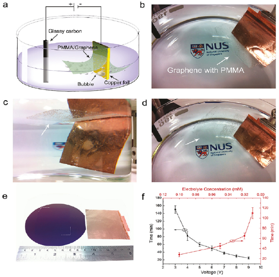
Figure VI.4. Electrochemical exfoliation of graphene from Cu. (a) Schematic diagram of electrochemical cell used for exfoliation, (b)–(d) optical images showing the 'whole film' peeling of PMMA-covered graphene form Cu. (e) Graphene film wet transferred onto a 4 inch wafer. (f) Time needed for complete film exfoliation of a 5 cm × 5 cm foil as a function of voltage and electrolyte concentration (at 5 V, red line). Adapted from [779], copyright American Chemical Society.
Download figure:
Standard image High-resolution imageUsing a custom-made mechanism (figure VI.4) (utility model P.411053) the Cu/Graphene/PMMA stack is placed in KCl, 1 mol dm−3, at a rate of 1 mm s−1 or an aqueous solution of K2S2O8 (0.05 mM) to perform the delamination. The graphene/Cu cathode is kept as the negatively polarized (from 4 to 10 V) and the anode can be made of a number of materials including glassy carbon. Hydrogen bubbles appear then at the graphene/Cu interface due to the reduction of water molecules and allow graphene to gently detach. The current depends on the Cu foil size and can be adjusted to control the delamination rate to ~1 mm s−1.
In order to obtain the best results, the samples are gradually immersed in the electrolyte solution at an angle ~45° as in figure VI.5. At this angle the graphene/PMMA stack slowly moves towards (floats) the top of the solution and the Cu foil moves toward the bottom of the glass container. After the delamination process, the detached Graphene/PMMA stack is rinsed with DI water, transferred onto the substrate, heated to 130 °C, and treated with acetone to remove PMMA. Next, graphene samples are dried for 1 h at high T (~350 °C) in high vacuum [851, 1010] or high pressure [1016] furnace to be sure that the organic residues and impurities are removed, although other methods claim no polymer residue [851, 1017]. After the delamination process, the detached Graphene/PMMA is rinsed with DI (deionized) water [1011], transferred onto the substrate, heated to 130 °C, and treated with acetone to remove PMMA. Additionally, UV-irradiation was suggested to facilitate PMMA rinsing [1018]. When substrates other than Cu are used to grown graphene, such as Ir, an additional step before the main electrochemical delamination process is needed. It was shown that an effective transfer could be achieved in SLG/Ir samples after treatment with a 0.1 M tetraoctylammonium-bromide TOABr/acetonitrile solution prior to the electrochemical delamination [1019, 1020]. Figure VI.5 presents the scheme of the graphene transfer process. Figure VI.6, shows the iteration of the transfer process to place MLG on PMMA [1021]. Ref. [1015] found that the delamination of graphene from Pt and Cu electrodes (substrates) increases with Na(OH) concentration, making this attractive as practical process to remove graphene from metal surfaces. More work is needed to bring this process from laboratory to 'production'.
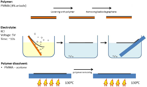
Figure VI.5. High-speed electrochemical delamination graphene transfer. Adapted from [1021], with the permission of AIP Publishing.
Download figure:
Standard image High-resolution image
Figure VI.6. (a) Images of stacks of 2, 4, 9, 12, 24, 37, 50 LGs on PMMA. (b) Optical transmittance of MLG stack.
Download figure:
Standard image High-resolution imageOne of the most difficult challenges are residues left by the PMMA used as the carrier µ. Ref. [1022] studied the surface of CVD graphene before and after transfer and compared it to HOPG. They found that there are significant organic residues that limit µ [851]. It is difficult to completely remove all impurities using only the organic solvent and the PMMA residue from the graphene surface. High-T treatment in high-vacuum is additionally needed for a more effective and cleaner transfer. To examine the effect of T during this treatment, x-ray photoelectron spectroscopy was used (see section IX.2/ARPES) to determine the chemical composition of graphene surface before and after heat treatment. A large O1s [812] peak on the XPS graphene spectrum before the heating is apparent in figure VI.7. An enhancement of the intensity of the characteristic C1s XPS peak located at 288.9 eV, which represents the C–C=O and O=C–O groups [812], is a signature of an incomplete PMMA removal. After heat treatment in 350 °C in high-vacuum, the C1s and O1s XPS peaks in figure VI.7 are the same as those corresponding to graphene samples that had never had been into contact with PMMA, confirming that the removal of the polymers is complete.
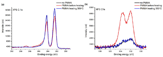
Figure VI.7. High resolution XPS C1s (a) and O1s (b) spectrum of transferred graphene samples before heating (red line), after heating (blue line) and graphene samples without contact with PMMA (black line).
Download figure:
Standard image High-resolution imageAn additional method for the confirmation of the PMMA residue removal is scanning near-field optical microscopy (s-SNOM) [1023, 1024] (see section IX.1/AFM for an introduction to the technique). Topography and near-field images recorded on graphene samples on SiO2/Si before and after heat treatment are shown in figure VI.8. After heating the graphene surface looks much cleaner, the wrinkles smoothen and the particles derived probably from PMMA are fewer. As the probing depth of s-SNOM is larger compared to the graphene thickness, the recorded optical contrasts show not only the local defects in the graphene layer but also differences in the substrate composition and in the distribution of the PMMA contamination

Figure VI.8. AFM and near-field IR images recorded from samples before (a) and after (b) heat treatment. Scan size for each measurement was 10 × 10 µm2.
Download figure:
Standard image High-resolution imageA spectroscopic method based on imaging an area at different wavelengths was used to test whether the contamination particles randomly spread across the graphene samples are indeed PMMA molecules. As the dielectric function depends on the wavelength [1025], the scattering coefficients (amplitude and phase) of the investigated materials varies with the tuning of the laser wavelength [1026]. Imaging at 1150 cm−1 illumination frequency, on resonance with the SiO2 vibration (asymmetric stretching vibration of the oxygen atoms bridging the Si-O tetrahedral groups) the optical contrast between graphene/SiO2 and PMMA particles is the largest. The near-field IR images recorded on a PMMA particle in figure VI.9 show a stronger phase at 1740 cm−1 due to the carbonyl band absorption at this wavelength [1027], while the optical phase on the graphene and substrate is larger at 1150 cm−1, matching the SiO2 phonon absorption [1028]. For both wavelengths, the optical amplitude (scattering efficiency) is stronger on the inorganic materials compared to PMMA, due to the lower reflectivity coefficient on the polymer [1029]. These measurement together with the XPS strongly suggest that the particle residue is PMMA.

Figure VI.9. Sequential imaging of a PMMA particle at 1130 cm−1 and 1740 cm−1. Scan size: 200 × 200 nm.
Download figure:
Standard image High-resolution imageRef. [1012] studied the use of rosin (C19H29COOH) as a support layer. The advantage is a high solubility in organic solvents, weak interaction with graphene, yet strong enough to enable support and transfer. These potentially make it a more suitable support in comparison to PMMA, as for the XPS data comparison of the transferred graphene using the two different materials [1012]. Therefore, through a combination of support material selection and surface treatment process/cleaning one can in principle create a graphene surface that is clean enough for many applications. The cleanliness needed will depend on the application.
Another way to ensure a clean graphene surface is to coat it with a metal or an oxide to eliminate the adhesion of any organic compounds. Ref. [1017] used Au as interface layer between graphene and PMMA and demonstrated a decrease in contact resistance of a factor of two. Ref. [1030] used Ti as an interface material to clean the graphene surface after transfer. Ti reacts with the residues on the graphene upon deposition. The 'reacted' Ti is then removed using a dilute HF solution. This also led to a decrease in contact resistance.
VI.1.2.1. Chemical delamination
There are two main techniques that have been evaluated to delaminate graphene from metals chemically: (1) Tetraalkylammonium (TOA)-assisted electrochemical delamination and (2) water delamination. The first is is a modified electrochemical delamination ('bubbling') method which enables the exfoliation of SLG and FLG or h-BN from substrates which are more strongly interacting than Cu [1031]. The TOA pretreatment was introduced in Ref. [1019] to enable the subsequent delamination of Graphene on Ir. Tetraalkylammonium compounds are weaken the interactions of sp2 materials with the underlying metal [1019, 1020, 1032], thus facilitating the subsequent detachment from the substrate. TOA+ intercalation is a 3-electrode electrochemical procedure which requires the use of a potentiostate to ensure a fine control on the bias between working and reference electrode. In the following, reference will be made to graphene grown on Ir, but the same protocol applies to many other LMs, including h-BN/Rh and MoSe2.
The experimental set up of the electrochemical cell can be seen in figure VI.10. The cell is open to the air or Ar atmosphere. The Working Electrode (WE) is the graphene/Ir sample. It is fixed to one corner by an alligator clip. The reference electrode (RE) is an Ag wire (alternatively one can use a standard Ag/AgCl or any other reference electrode, in which case one needs to correct the bias between WE and RE to account for the potential offset of the RE). The Counter Electrode (CE) is a Pt wire. The WE and the RE should be placed as close as possible facing each other (avoiding contact); the CE should be facing the WE (with the RE between the two) and should be immersed in such a way to expose a large area. The operation of the vessel follows several steps. Fill the vessel with 10–20 ml of TOABr/acetonitrile solution (0.1 M concentration, i.e. 5.46 g of TOABr every 100 ml of solution). Subsequently, degassing the solution with Ar or N2 for 15 min is required. After, leave the Ar/N2 capillary tube above the vessel, in order to maintain an Ar or N2 atmosphere and prevent air from dissolving into the solution. Then, apply −1.9 V between WE and CE for 10 min to promote TOA+ to the graphene/metal interface. A partial discharge of the sample for 20 s at −0.2 V follows to obtain Ir/TOA/graphene stack. This step is needed to prevent the negatively charged graphene from reacting with the PMMA and facilitate subsequent PMMA removal.

Figure VI.10. 3-electrode setup used in TOA intercalation and voltammetry experiments. Adapted from [1020], with permission from AAAS.
Download figure:
Standard image High-resolution imageAfter TOA-pretreatment, the samples must be rinsed in acetonitrile, dried in N2 atmosphere, and spin-coated (or drop-coated) with PMMA. The samples can be then exfoliated according to the electrochemical delamination explained above [1021].
Water intercalation has also been found to be an effective method of decreasing the bonding between graphene and underlying metal substrate [1033]. In this process, water is intercalated between metal substrate, e.g. Pt, and graphene. The intercalated graphene film/metal substrates is then placed on a hydrophilic SAM surface, dry bonded and transferred through an electrolysis process. This process enables the reuse of the growth substrate without significant metal loss.
VI.1.3. Electrochemical oxidation by cyclic voltammetry
Electrochemical oxidation can be described in terms of the formation of a metal-oxide layer at the interface between graphene and metal. A rational optimization of the parameters of this process follows the methodology described below. The voltammetric profile of Pt in a non-adsorbing electrolytes is known [1034], but the conclusions can be extended to other metals. It was reported [1035] that the processes that occur at the metal surface can be described by the reaction

where * stands for a free Pt adsorption site. In a first step, the water molecules interact with the graphene/Pt electrode, intercalating through graphene, then dissociate in the Pt surface forming Pt2(OHads). A charge ~101.50 µC cm−2 is transferred, corresponding to the formation of Pt2(OHads) with a coverage close to 1 monolayer. Even though SLG presents a barrier to direct access to the metal surface, the water molecules are able to diffuse onto the metallic substrate via surface defects [1036]. The intercalated water between SLG and metal surface is responsible for the oxidation of the outermost Pt atoms when an appropriate potential is applied.
Voltammetric measurements were performed under N2 in a three-electrode set up (figure VI.11) [1037]. There is a N2 gas inlet and outlet to assure an inert environment during the electrochemical oxidation. A Pt wire (99.99% purity) serves CEand all the potentials are quoted with respect to the Ag/AgCl (RE. The Ag electrode is specific for the cell (Ag/AgCl electrode driref-25H, WPI). The WE is the Pt(1 1 1) sample covered with a SLG. The WE area exposed to the solution is 0.33 cm2 in all experiments. The electrochemical cell is set into a Faraday cage in order to reduce the signal-noise ratio. The electrolyte employed is 0.1 M HClO4 and the water is purified with a Millipore Milli-Q purification system. A scan rate of 0.05 V · s−1 is selected to control the oxidation reaction. The anodic potential is varied to obtain the optimal conditions to decouple graphene from Pt avoiding side reactions, such as the evolution of CO2 and O2, and defects in the graphene network. The sample is placed on the electrochemical cell for 1.5 h soaked into the previously deoxygenated acid solution so water molecules are able to diffuse onto the metallic substrate via surface defects [1036]. Figure VI.12 shows four cyclic voltammograms with different experimental conditions used to decouple an area ~0.33 cm2 of graphene from Pt(1 1 1).The first protocol (A, figure VI.12(a)) is an anodic potential scan from 0.36 to 1 V followed by a cathodic potential scan between 1 V to 0.7 V. The second B, figure VI.12(b)) is similar, but with a higher applied potential (1.05 V). In the third cycle (C, figure VI.12(c)) the potential is even higher (1.45 V). In the last one (D, figure VI.12(d)) two cycles are involved: a complete oxidation-reduction in the range 0.45–1.1 V and a subsequent oxidation up to 1.1 V, followed by reversing the potential finishing at 0.7 V. The applied potential in A is not high enough to decouple graphene. D is the most aggressive and the sample is decoupled but also damaged. B and C accomplishthe best decoupling, meaning that every method in between those ranges will be appropriate to decouple graphene from Pt.
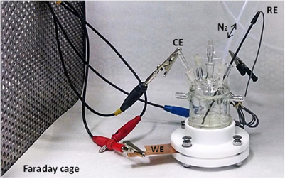
Figure VI.11. Electrochemical cell used for the electrochemical oxidation of Pt in the Graphene /Pt (1 1 1) stack. RE, is the Ag/AgCl reference electrode, CE the Pt counter electrode and WE the working electrode (i.e. stack graphene/ Pt(1 1 1). The cell is purged with N2 and installed inside a Faraday cage.
Download figure:
Standard image High-resolution image
Figure VI.12. Cyclic voltammetries for graphene on Pt(1 1 1) in 0.1M aqueous HClO4 solution. Four different voltammetric treatments have been applied (A, B, C, D), being the scan rate 0.05 V · s−1 in all the cases. The right panels plot the potential programs applied to the SLG/Pt electrodes, producing the corresponding cyclic voltammograms of the left panels.
Download figure:
Standard image High-resolution imageTable VI.1 summarizes the potentials and scan rates for the shown cyclic voltammograms. It also includes the parameters to oxidize Pt and the charge involved in the oxidation process, as well as the charge to get 1 monolayer of Pt2OH. The presence of SLG delays the oxidation process compared with the clean Pt(1 1 1) sample, requiring higher overpotentials to attain a comparable oxidation charge. The charge obtained by integrating the anodic peaks for the other treatments is lower in comparison with the target. The process starts when the oxide coverage is much less than one monolayer (~0.25 of monolayer). Table VI.1 also includes the parameters to decouple graphene from Ir(1 1 1).
Table VI.1. Parameters for potential-controlled electrochemical oxidation of Pt(1 1 1) and Ir(1 1 1) with SLG on top. Ei stands for the initial potential, Esup for the upper limit of the potential, Ef for the final potential, v for the scan rate and Q for the charge.
| Ei (V) | Esup (V) | Ef (V) | v (V · s−1) | Q (µC · cm2) | ||
|---|---|---|---|---|---|---|
| 1 ML Pt2OH | 120 | |||||
| SLG/Pt(1 1 1) | A | 0.36 | 1 | 0.7 | 0.05 | 10 |
| B | 0.36 | 1.05 | 0.7 | 0.05 | 32 | |
| C | 0.36 | 1.45 | 0.7 | 0.05 | 106 | |
| D | 0.46 | 1.1 | 0.7 (cycle and a half) | 0.05 | 24 | |
| Pt(1 1 1) | B | 0.36 | 1.05 | 0.6 | 0.05 | 101.5 |
| Gr/Ir(1 1 1) | 0.2 | 1.0 | 0.9 | 0.05 | 140.8 | |
VI.2. Semi-dry transfer: hot press lamination and UV assisted transfer
UV adhesive (UVA) and hot-press lamination (HPL) [1040], which can be broadly classified as semi-dry transfer. This is the process of transferring graphene without complete immersion of substrate and graphene in an aqueous environment [115]. In particular this refers to the use of melt techniques whereby a liquid interfacial layer is solidified by various means [1759]. Both methods are large-area-compatible [115], and are capable of producing transferred layers that are optically transparent and electrically conductive whilst retaining areal uniformity with only a few percent variation. UVA and HPL are stable under bending stress and fatigue with a resistance towards micro-crack formation compared to ITO and FTO platforms [1760].
Figure VI.13(a) outlines the HPL process [1040]. Thermally activated ethylene vinyl acetate (EVA) treated PETsubstrate were used, however other supports such as thermal release tape (TRT), with different adhesive strengths ranging from 2.5 to 7.0 (N/20 mm), can be also used. First, the as-synthesized graphene-on-Cu stack is sandwiched between the polymer and a 125 µm-thick PET substrate, the acting as mechanical support. The sandwich structure then traverses a dual roller laminator, which is, contingent on the laminate used, either cold [1761] or heated to ~100 °C [1040]. Following lamination, the backside laminate, i.e. the side in contact with the heated stage during CVD, is mechanically detached. This exposed graphene-coated-Cu face can then be ashed to remove residual organics along with the defective graphene layer. The Cu catalyst is then etched, in this case, using (NH4)2S2O8 in de-ionised (DI) water (1 M) for 12 h. The transferred films are subsequently rinsed in DI water and dried in high-purity N2. Up to 0.1 m2 areas were transferred using this method, though larger areas and subsequent integration into roll-to-roll process lines are easily accommodated. EVA is also suitable for flexible substrates, which cannot withstand solvents such as acetone and/or isopropyl alcohol [1762]. Following transfer, the resulting polymer/graphene stack remains attached to the target substrate. Repeated lamination, at RT or elevated T, can be undertaken to further remove absorbates, bubbles, voids and non-conformalities in the transfer [1719, 1720]. In the case of TRT, the support-coated substrate is finally baked at 120 °C to remove the TRT.
Figure VI.13. Graphene transfer by (a) HPL and (b) UVA, and (b) corresponding optical images and (c) and (d) 550 nm optical transmission maps. Adapted from [1038–1040].
Download figure:
Standard image High-resolution imageFigure VI.14(b) outlines the UVA transfer [1040]. The UV adhesive is first coated onto a polymer substrate by spin coating at 5000–8000 rpm for 30–60 s, following a preliminary casting at 500 rpm for 10–20 s. This coated substrate is then placed in contact with the as-grown graphene-on-catalyst. This sandwich is subsequently compressed at 0.2 MPa using a cold-roll laminator, to avoid air pocket formation at the interface. The UVA is subsequently cured by exposing the backside of the PET to a UV optical source (365 nm, 20–25 mW m−2) for 10–15 min. The Cu foil is etched in aqueous ammonia persulfate for 12 h, rinsed in DI water and dried in high-purity N2. All at RT, making the approach applicable to a wide range of polymer substrates. Figure VI.14(c) shows typical optical micrographs of transferred samples that exhibit long-lasting adhesion between substrate and graphene[1040].
Figure VI.14. (a) Change in normalised resistance (ΔR/R0) with bend radius. (b) 〈ΔR/R0〉 for all bending diameters for UVA, HPL, PMMA and ITO. (c) peel strengths for transfer methods. Inset: Typical AFM height maps of fatigued transfers. Adapted from [1038–1040].
Download figure:
Standard image High-resolution imageVI.2.1. Benchmarking and ageing effects
Ref. [1040] reported that the optical transmittance (%T) for HPL and UVA transfers was ~10% and 12% lower than the uncoated substrates. This was assigned [1038–1040] to the transferred graphene and the augmented optical properties of the interfacial binding layer. The spatially averaged 550 nm transmittance of HPL and UVA is ~58.6% ± 3.6% and 76.5% ± 3.8%, respectively [1040]. Both techniques result in equivalent areal uniformity with <4.0% variation. The increase in absorption is likely due to folding and wrinkling of graphene during transfer. Ref. [1040] reported a rms of HPL ~26% higher than UVA. The agglomerates, 5.5 ± 5.6 µm (UVA) and 7.9 ± 3.9 µm (HPL), are most likely adhesive residues.
Using PMMA transferred graphene on quartz, with Cr/Au van der Pauw structures on the order of tens of micron in channel size, graphene showed Rs~5.47 ± 1.20 kΩ sq−1. Rs for HPL transfers was ~9.9 ± 3.8 kΩ sq−1, whereas UVA showed lower values ~3.5 ± 2.3 kΩ sq−1 [1040]. Elemental analysis revealed significant (S) and (O) peaks in UVA transfer, attributed to Cu etchant exposure [1763]. Such peaks were absent for HPL transfers [1764]. S is a strong dopant of graphitic carbons [1765].
The 550 nmtransmittance of UVA transfers tends to increase with time (~80%) [1040]. No observable change was reported for HPL transfers, likely due to the absence of doping. The metallic component of may be central to the doping temporal stability [1039].
HPL transfers were reported with a time invariant Rs (5.0 → 5.2 kΩ sq−1), whereas Rs of the UVA transfers increased from an initial 2.2 kΩ sq−1 to 3.5 kΩ sq−1, after 200 h, suggesting the need for an hermetic capping layer [1766]. Such deleterious increase in Rs in due to time and ambient unstable Sdoping associated with the necessary Cu-etching. Rs doped graphene remains approximately one order of magnitude larger than achieved by doping strategies reported elsewhere [1051, 1041, 1042]. This may be, in part, associated with the macroscale measurements undertaken, and the necessarily higher areal density of defects within the measured channels.
To attain a robust mechanical interface, graphene requires proximal contact to the substrate [1767]. In both transfer approaches, the as-grown graphene-on-catalyst achieves contact the EVA melt and to low-viscosity UVA prior to curing. Graphene transferred in this way showed lower surface energy and higher adhesion (UVA: 4.40 ± 1.09 N m−1, HPL: 0.60 ± 0.26 N m−1) compared to PMMA transfers (PMMA: 0.44 ± 0.06 N m−1) [1040].
To assess the bending fatigue performance, transfers were assessed during 104 bend cycles with the differential resistance extracted after each (figure VI.14(b)) [1040]. ITO on PET showed a 95-fold increase in differential resistance, up to ~190 kΩ. After such testing, the fatigued ITO showed a significant difference in resistance between its bent and relaxed state. The differential resistance of graphene, in both UVA and HPL increased from ~46 kΩ to 74 kΩ, with less than ±0.5 kΩ difference between bent and relaxed states [1040], highlighting the robustness in maintaining electrical continuity even after many thousands cycles. The is was~60 times higher than ITO/PET.
The differential resistance as a function of angle and bend radius was also investigated (figure VI.14(b)) [1040]. All transfers demonstrated a low normalized resistance even at bend angles ~100° (1.05, PMMA; 0.94, UVA; and 1.04, HPL), almost two orders of magnitude less than optoelectronically comparable ITO on PET (79.8) [1768]. The mechanical robustness of transferred graphene is, regardless of the transfer method, much improved over ITO. UVA transfer showed consistently lower resistance for all bend angles, though HPL graphene repeatedly showed the lowest for bend angles >40°. These bend angle experiments suggest that UVA and HPL are somewhat more robust than PMMA in high-bend-angle applications, such as e-paper and wearable sensors. For bend radii Rb = 1 − 5 mm Ref. [1039] reported that ITO normalised resistance increased ~20/90 at Rb = 5/1 mm. Conversely, the change in the normalised resistance of all graphene transfers, including PMMA, were much smaller (PMMA: 0.5 − 0.9, UVA: 0.5 − 0.8, and HPL: 0.2 − 1.2) and showed no measurable dependence on Rb for the bend radii considered. UVA and HPL approaches seem to offer a viable solution to the limited flexibility, with maintained conductivity, of transparent electrodes used in flexible electronics.
T-peel tests were also conducted to explore the level of adhesion between graphene and flexible substrate [1769]. A low peel strength represents weak adhesion between laminate and substrate, while a high peel strength suggests that graphene is strongly adhering. As depicted in figure VI.14(c), UVA-transfers showed the highest peel strength (4.39 ± 1.09 N m−1), followed by HPL (0.60 ± 0.26 N m−1) and PMMA (0.44 ± 0.06 N m−1).
VI.3. Dry transfer using h-BN
A contamination- free transfer process utilizes exfoliated hBN flakes to pick up graphene from Cu [823, 832]. Figure VI.16(a) is an optical microscopy image of a graphene crystal on Cu, exposed to ambient conditions for a few days, resulting in the oxidation of the interface between Cu and graphene. The oxidation of the interface does not only make the graphene optically visible, but also decouples it from the substrate.
For the transfer process, a polymer stack consisting of PDMS, PVA and PMMA is prepared. First, a glass slide is covered with scotch tape and drop coated with a 13% aqueous solution of PVA and baked at 95 °C for 5 min. Subsequently, the slide is spin coated with PMMA (4%, 50 k, in ethyl lactate) at 1000 rpm and baked for 10 min at 110 °C. Then, h-BN is exfoliated on the PVA and large, thin and defect free flakes are selected and cut out in a 5 mm × 5 mm square. The polymer stack can be lifted off the scotch tape using tweezers and placed on a 3 mm thick cushion of PDMS, resting on a glass slide. As depicted in figure VI.15(b), the h-BN is aligned with a graphene flake brought into contact and heated to 125 °C. During the cool down (at ~75 °C), the polymer and Cu foil are separated again, resulting in an h-BN flake covered with graphene on the polymer stamp. Next, an arbitrary substrate, e.g. an h-BN flake on Si/SiO2, is aligned with the h-BN/graphene stack, brought into contact at 125 °C and peeled off the PDMS. Subsequently, stack of SiO2/h-BN/graphene/h-BN/PMMA/PVA is placed in hot water, acetone and isopropanol, in order to dissolve the polymers. Figure VI.15(c) depicts such an h-BN/graphene/h-BN sandwich on a SiO2 substrate.
Figure VI.15. (A) Graphene crystal onCu grown as described in section VI.1.2. after exposure to ambient conditions for several days. (B) Schematic of dry transfer. (C) h-BN/Graphene/h-BN fabricated using contamination free dry transfer. Panel (B) is adapted from [832], with permission from AAAS. Panel (C) is adapted from [823], copyright American Chemical Society.
Download figure:
Standard image High-resolution imageVI.4. Graphene/PMMA sandwich structures
Removing PMMA after transfer is not allways necessary as there are potential benefits of building graphene/PMMA heterostructures [1040]. PMMA is a colorless polymer, commonly used as a glass replacement (acryl glass). Very thin, transparent PMMA could be beneficial. The dielectric constant of PMMA is 2.6 and comparable to fused silica (~3.5) [895], making PMMA a decent insulating layer between multiple graphene layers. PMMA has been used to prevent the contact of graphene with water during transfer, therefore enabling the use of water-sensitives substrate and in applications to fabricate flexible, air-stable, low-voltage GFETs [1043]. A polymeric bilayer consisting of PBU (bottom) and PMMA (top) can be used as a supporting layer for graphene transfer without affecting its promising intrinsic characteristics [1770]. The Dirac voltage and field-effect µ of GFETs with the polymeric layers kept the intrinsic properties of graphene unaltered in air for more than 130 days, whereas GFETs without polymers underwent significant and rapid degradation. High resolution positive tone electron beam resists, ARP-661.08 and ARP-672.08 (by Allresist(tm)), have been used to build PMMA/Graphene heterostructures [1044, 1045]. ARP-661.08 has molecular mass ~600 000 g mol−1 and requires chlorobenzene as a solvent or a thinner, while ARP-672.08 has molecular mass ~950 000 g mol−1 and requires anisole as a thinner. Both thinners consists of a benzene like structure and are small size weight ~110 g mol−1). The higher molecular mass of ARP-672.08 can increase the resist film durability, which can be beneficial if the resist film needs to be transferred or made free standing. When the PMMA/Graphene film is deposited on a substrate, long PMMA molecules can be reduced in size by electron beam lithography [904, 1046]. This may open up an interesting route for graphene patterning [1046].
PMMA layers with thickness ~600–800 nm have been used in heterostructures [1044]. After spin coating, Cu/graphene/PMMA was baked at 60 °C for 10 min to evaporate most solvents. The transition temperature of PMMA from soft polymer to acryl glass is ~100 °C [904]. Similar recipes can be used to transfer the PMMA/Graphene hybrid or as a free standing. Elastic and thin graphene/PMMA films can be stacked [1044]. Figure VI.16 shows a free standing 500 nm graphene/PMMA sandwich placed on an Al aluminum plate with 10 mm diameter hole. The sample is prepared by using ARP-672.08 resist (4.5% diluted with anisole). Similar 1 µm thick free standing films were fabricated using ARP-661.08 (4.5% diluted with chlorobenzene) [1045].
Figure VI.16. Free standing 500 nm thick and 10 mm in diameter graphene/PMMA structure. The film is transparent and thus convenient for optical experiments.
Download figure:
Standard image High-resolution imageMulti-layered structures, where graphene is sandwiched between two PMMA layers, can be prepared and used as EMI shielding layer by absorbing >50% of electromagnetic waves at 30 GHz [1044].
VII. Growth and transfer of other layered materials
VII.1. Hexagonal BN
BN, has been extensively studied as a dielectric material for LM-based devices It has a large bandgap (>6 eV), atomic flatness, chemical inertness and small lattice mismatch (1.8% larger) with respect to graphene [1047]. H-BN is a natural dielectric to GRMs as SiO2 and Si3 N4 are to Si-based devices. The quality and structural characteristics of the hBN film can impact the performances of GRM-based devices. h-BN bulk single crystals, are very small, millimiters at most, and do not satisfy manufacturing requirements. In order to meet future, GRM based device manufacturing requirements, it is necessary to develop processes capable of providing large area single crystal or polycrystalline films that can meet both device and high volume production needs. The growth process selection depends on the materials requirements. Up to now most devices have used multilayer h-BN with only a few using monolayer films. It is likely that many applications will require multilayer films rather than 1L-h-BN, and some applications can use use polycrystalline films. The exact requirements will guide the selection of the film growth/deposition process.
Hexagonal hBN has been grown on metals, dielectrics and graphitic surfaces by various techniques and under different conditions. The basic growth techniques used so far are the following: (1) growth on dielectrics and graphitic surfaces by CVD and PA-MBE; (2) growth on metals by a diffusion and precipitation as well a surface limited processes; (3) Growth by ion beam assisted deposition and by physical vapor deposition. Each of these have advantages and disadvantages. When considering the use of any material for devices it would be desirable to deposit or grow it at low T on a desired surface as done for materials integrated in Si-based devices. In the case of GRMs it has been difficult so far to integrate/grow/deposit the m directly on the desired surface in a fully integrated flow. This issue has necessitated the development of specific film transfer processes which will be discussed a the end of this section. Therefore, the selection of a growth process will depend on whether the materials requirements can be met to satisfy the specifications of the individual application and on whether the material will be transferred or grown/deposited on the device being fabricated.
VII.1.1. Growth of h-BN on metal surfaces
h-BN was grown on Cu foils by LPCVD in a horizontal reactor using ammonia borane as BN source and H2 as carrier gas [1049]. The growth of h-BN on metals can be carried out in a hot-wall low-pressure ~10−3 mbar reactor, vertical or horizontal, as for figure VII.1. This process can be redesigned to a vertical furnace batch type reactor commonly used by the semiconductor industry. Borazine is a volatile liquid with a relatively high vapor pressure (280 mbar at 25 °C), and is air and moisture sensitive [1050]. Therefore, its use requires a specific set-up to have an accurate control of the gas flow. To avoid gas flash in the CVD chamber and have good control the flow rate, borazine is maintained at 0 °C with a chiller to control the vapor pressure and a system of mass flow controllers is used to transport the gas to the growth chamber. A cold trap was installed to prevent the damage of the scroll pump with potentially non-decomposed borazine. The process follows the typical cycle of heating, pre-annealing (30 min under H2 at 1000 °C) of the metallic substrate, usually polycrystalline Cu or Ni, growth at 1000 °C, a regulated pressure of 0.3 mbar, under 50 sccm of H2, with Pborazine = 10−2 mbar, for a time between 10 min and 2 h, and slow cooling under H2 flow.
Figure VII.1. Schematic diagram of vertical CVD growth chamber for hBN growth on metal.
Download figure:
Standard image High-resolution imageThe role of the underlying metal, Ni and Cu, microstructure on the BN film morphology was studied. Figure VII.2(a) shows an optical image of a BN film grown on Cu and transferred onto a 90 nm SiO2/Si. Yellow and pink areas correspond to folded edges of BN. The thickness of the film determined from the AFM profile is ~70 nm, with a 20 nm roughness (figure VII.2(b)). This behaviour is confirmed by TEM observation of the sample (figure VII.2(c)). The electron diffraction pattern, figure VII.2(d), shows several six-fold symmetry patterns and diffuse rings, indicating that the film is crystalline and turbostratic. This result is in agreement literature in the same range of T and borazine partial pressure [1051, 1052], for which a non self-limited growth, with a turbostratic stacking is expected. Due to its non-flatness and turbostratic structure, this hBN useful as a graphene substrate, as well as being good candidate to be used as dielectric compatible with GRMs as capping material in a device.
Figure VII.2. (a) Optical image of BN film grown on Cu and transfer red onto 90 nm SiO2/Si, scale bar is 50 µm. (b) AFM profile showing the 90 nm thickness and the high roughness. (c) TEM image with scale bar 4 µm and (d) electron diffraction pattern showing the rough/turbostratic nature of the ML-h BN film grown on Cu with scale bar 5 nm.
Download figure:
Standard image High-resolution imageHigher crystallinity is achieved if h- BN is grown on Ni [1053–1056] as compared to the growth on Cu. Few investigations were performed to elucidate the influence of the underlying Ni grain orientation on the BN growth kinetics and coverage but there is hardly any record in terms of crystallinity, morphology and thickness of the BN film [1057, 1058]. In order to fully characterize the influence of the grain orientations of the substrate on the BN film structure, combined SEM and TEM imaging and electron diffraction of both BN film and underlying Ni substrate are used. Figure VII.3(a) is a SEM image of the as-grown BN on its substrate showing an area at the intersection of three differently oriented Ni grains. Their respective crystalline orientation is determined by Electron Back Scattering Diffraction (EBSD) in figure VII.3(b). Two different surface aspects of the film can be identified and are dependent on the Ni orientation. In the blue grain with a (1 1 1) orientation, the film surface structure is striated and nearly smooth, while for other orientations (0 0 1), red grain, the surface appears to be very rough. Direct transfer on the TEM grid enabled TEM observations of the same area. The TEM image of figure VII.3(c) reveals the effect of Ni grain boundaries on the BN film and confirms the presence of different BN morphologies depending on the underlying Ni grain orientation: flat and rough [1059]. As on Ni (1 1 1) hBN displays an almost perfect lattice match, the BN growth is highly oriented resulting in the formation of a flat h-BN as shown in figure VII.3(c). By recording electron diffraction patterns in different areas as shown in figure VII.3(d), the single crystalline character of the h-BN film over the whole Ni (1 1 1) grain is assessed. For (0 0 1) Ni grain orientations, the h-BN growth domains nucleate at different places on the Ni surface and grow independently from each other. This process is responsible for the island morphology characterized by thickness variations from an island to another, discontinuity between the islands (darker and brighter contrast on TEM image figure VII.3(e)) and multiple orientation domains (several rotated electron diffraction patterns, figure VII.3(f)).

Figure VII.3. (a) SEM image and (b) corresponding EBSD mapping of BN on Ni. (b) TEM image of the BN film transferred polymer-free on holey amorphous carbon TEM grid. HR TEM images and corresponding electron diffractions of (c) and (d) a flat BN area and (e) and (f) a rough BN area with the schematic of the growth process: Van der Merwe for Ni(1 1 1) and Volmer Weber for Ni(1 1 0) and Ni(0 0 1).
Download figure:
Standard image High-resolution imageThis detailed analysis presented above on the growth of h-BN on polycrystalline Cu and Ni provides insights and guidelines for further optimization of the h-BN conditions leading to planar and single crystal layers needed for many applications.
The growth of h-BN at atmospheric pressure CVD (APCVD) may reduce the production costs of h-BN. Ref. [1062] synthesized h-BN by APCVD on polycrystalline Ni. Depending on growth conditions, the thickness of the obtained h-BN film is between ~5 and 50 nm with grain size limited by the size of the Ni single crystal grains. The controlled growth of h-BN on polycrystalline Pt foils by APCVD with ammonia borane as the precursor was also reported [1061]. 1L, 2L and FL-h-BN domains and large-area films were selectively obtained on Pt by changing the concentration of ammonia borane. 1L and 2L h-BN obtained are uniform with high quality and smooth surfaces.
In principle the quality of h-BN can be significantly improved by growing on single crystal metals. h-BN on Rh(1 1 1) (h-BN nanomesh) was first reported [1062]as well as on Rh(1 1 1)/YSZ-buffered/Si(1 1 1) [1063]. This substrate formation strategy may also be considered as a model system for growth of 1L- h-BN on transition metals (catalyst) surfaces at T < 1000 K. BN nanomesh has been extensively studied, starting from pure surface science [1062] to applications as electrodes in electrochemistry [1064, 1065] and exfoliation [1066]. It was used as a template for molecular assemblies in vacuum [1067], and is stable in air and in liquids [1065, 1067]. It was furthermore used to study the effects of hydrogen [1064, 1068] and metal intercalation [1069].
The h-BN nanomesh is a corrugated honeycomb superstructure and is the product of a high T CVD growth using (HBNH)3 as a precursor. The highly regularly corrugated structure with a lateral periodicity of 3.2 nm is determined by the mismatch between hBN and Rh. The unit cell consists of 13 × 13 BN units on 12 × 12 Rh atoms. It has one 'pore' with 2 nm diameter, and is surrounded by 'wire' regions [1062, 1067] (figure VII.4(c)).The high T CVD growth of h-BN nanomesh on Rh(1 1 1) single crystal or Rh(1 1 1) single crystalline films on YSZ-buffered Si(1 1 1) wafers [1063] proceeds as follows. The substrate is first cleaned in UHV by Ar+ sputtering (1.0 keV, 3.5 µA cm−2 sputter current) for ~30 min, and annealed to 700 °C. The substrate is kept at 700 °C for 5 min, and oxygen (P(O2) = 5–8 × 10⁻⁷ mbar) is dosed for 10 min. This is followed by a flash-annealing treatment up to 900 °C for 5 min. The substrate is then cooled to RT. The whole preparation cycle (sputtering + annealing + O2 dosing + flash-annealing) must be repeated twice to ensure high quality of 1L-h-BN on Rh(1 1 1). At the third treatment cycle, no O2 dosing is needed. The substrate is directly flashed to 900 °C for 5 min after annealing. Then the substrate T is stabilized at 800 °C, and borazine is dosed at P = 5 × 10⁻⁴ mbar for 5 min. Afterwards the sample is cooled to RT with an initial cooling rate of 10 °C min−1. The YSZ/Si(1 1 1) substrates may be coated with a large number of unary [903] and binary transition metals, which allows the tailoring of the growth products. The intercalation of other metals, such as like Au, was studied [1069]. On the binary transition metal PtRh it was found that the nanomesh unit cell may be tuned from 3.2 to 2.7 nm when increasing the substrate lattice constant from Rh to PtRh [1070].
Figure VII.4. (a) 800 °C hot 4 inch wafer in the growth chamber. (b) Low energy electron diffraction (LEED) pattern of h-BN/Rh(1 1 1) at 60 eV kinetic energy. (c) STM image of the same surface with Ut = −1.2 V and It = 0.5 nA.
Download figure:
Standard image High-resolution imageVII.1.2. Growth of h-BN on graphitic and dielectric surfaces
It would be advantageous to to grow h-BN on dielectrics or graphitic surfaces in the absence of a metal catalyst to satisfy device integration requirements for many applications. Direct growth of h-BN layers on graphite substrates was achieved using high T plasma-assisted MBE [1071]. The h-BN grown on HOPG is hexagonal with no chemical intermixing with the graphitic carbon layers. This processes seems to provide high qualtiy commensurated growth of h-BN on graphite.
There are reports on the direct growth of Graphene/h-BN heterostrutures. Ref. [1072, 1073] took advantage of the solubility of C in Ni to grow a graphene/h-BN heterostructure by a combination of C precipitation and MBE of h-BN on Ni/MgO(1 1 1). The growth process was performed first by saturating Ni(1 1 1)/Mg(1 1 1) with C, then growing h-BN on the exposed surface at high T (>730 C). The process can yield FLG/FLG-hBN heterostructures. The greatest difficulty is the control of thickness of both graphene and h-BN at the 1L level. While h-BN may be desired as a FL film, in most applications the graphene layer number would have to be precisely controlled (N = 1 ± 0, N = 2 ± 0, etc).
Ref. [1074] grew wafer-scale and high-quality ML-h-BN on sapphire by LPCVD. Spectroscopic and microscopic measureements revealed that the h-BN film had a wrinkle-free surface and AA' stacking, with a single orientation and a well-oriented superstructure with respect to sapphire. The electron transport in a GFET on h-BN/SiO2 was improved compared to SiO2. Ref. [1076] claims that these h-BN films can be transferred to any substrate making LMhs and LM-based electronic devices possible.
h-BNfilms were also successfully grown on (0 0 0 1) sapphire by metalorganic vapor phase epitaxy (MOVPE) [1075]. These were grown using triethylboron, B(C2H5)3, and ammonia (NH3) at various V/III ratios, ranging from 210 to 2100. The films grown at V/III ratios above 1280 showed two XRDpeaks, one from the (0 0 0 2) plane and the other from the (0 0 0 4) plane. These films also exhibited a Raman hBN peak at 1366 cm−1. In contrast, the films grown using V/III below 640 revealed an XRD pattern consistent with a turbostratic structure.
VII.1.3. Growth of h-BN by ion beam assisted deposition on metals and dielectrics
An alternative method of hBN growth is the physical vapor deposition (PVD) using a solid boron and nitrogen gas. This is not self-limiting, therefore the h-BN thickness can be controlled through the deposition time. This technique allows the deposition of thick layers of amorphous BN or cubic BN with different orientations and textures on almost any type of substrate, both metallic or insulator.
Among the possible PVD techniques, ion beam assisted deposition (IBAD) is specially versatile because it permits independent control of B and N fluxes, and fine tuning of the ion energy. The technique relies on electron beam evaporation of boron in vacuum and the simultaneous bombardment with N ions, [1076–1080]. Figure VII.5, depicts a typical experimental set up. BN is obtained in a vacuum by reaction between the evaporated B and the  ions. By using this technique, one can control the quality, texture and thickness of the h-BN layer by proper selection of growth parameters such as B/N impinging ratio, evaporation rate, deposition time, ion energy and substrate T. The composition of BN is adjusted by controlling the incoming B and N fluxes. The B/N ratio can then be measured by EDX, XPS, as shown in figure VII.6, and XANES,

Figure VII.5. IBAD set up.
Download figure:
Standard image High-resolution image
Figure VII.6. XPS from a stoichiometric h-BN produced by IBAD.
Download figure:
Standard image High-resolution imageTypical growth rates range from 0.1 to 10 nm min−1. Since the growth is not self limited in this process the thickness is controlled by the various deposition variables including deposition time. The quality of BN is determined principally by the substrate T and the ion energy, which controls the orientation of the basal planes, the defect density and surface roughness. A review of these parameters with regards to the formation of high quality h-BN: orientation, crystallite size and density of defects is given in Ref. [1081]. The deposited materials have been thoroughly characterized using spectroscopic analytical tools [1079, 1082–1085]. One of the most important properties is the extreme flatness, with a surface roughness ~0.1 nm for any film thickness.
VII.1.4. Transfer of h-BN
The goal of the transfer process is to get GRMs on suitable host substrates.
Transfer processes are based on the use of a temporary support, most of the time a polymer, as described in section VI for graphene. Several methods have been developed: (1) wet transfer, involving the use of a liquid aqueous solution, and (2) dry transfer, relying on solid adhesive layers. The second approach ensures the absence of water between layers, which can be detrimental to device properties. Table VII.1 scrutinizes advantages and drawbacks or difficulties inherent to both kinds of transfer processes.
Table VII.1. Comparison of the various procedures developed to date for transferring CVD grown BN.
| Method | Metals | Potential contamination | Special equipment | Re-use of the substrate | Time | Key parameters | Other | |
|---|---|---|---|---|---|---|---|---|
| WET | Chemical etching | Cu [1049, 1087], Ni [1054, 1058, 1062] | Etchant, polymer, metal residues, interfacial water | No | Several hours | Etchant nature and concentration | ||
| Electrochemical delamination (ECD) | Cu [1088], Pt [1061, 1189], [108, 1090] Fe [1091] | Electrolyte, polymer, metal residues, interfacial water | 5 V DC generator | Yes (smoothed) | A few minutes | Voltage, electrolyte nature and concentration | Possible damage due to gas bubbles produced at the interface | |
| TOA treatment + ECD | Rh [1066], Ni | ions, electrolyte, polymer, metal residues, interfacial water | 3 electrodes set-up | Yes | ~20 min | Voltage, electrolyte nature and concentration | ||
| Lift-off transfer | Cu [1092] | NaOH residues, polymer, metal residues, interfacial water | Yes | 2–3 h at 60 °C | Interface oxidation | |||
| DRY | PMMA/PVA [832] | Potentially any (depends on the interaction BN—substrate) | PMMA | Heating plate | Yes (if no BN remaining) | ~2 h | PMMA adhesion | Semi-dry transfer: water at the very end |
| Scotch tape | Adhesive residues | A few minutes | Scotch tape choice | Difficult release/deposition | ||||
Several parameters can impact the feasibility and quality of transfer, including the roughness and the thickness of the film, its homogeneity, the interaction with the substrate, and roughness and surface termination of the host substrate. These parameters determine best suited transfer for a particular growth on an specific substrate as it rules the basic properties of the grown film, (mechanical, defect density...) and interaction of film with growth surface and temporary support.
VII.1.5. Wet transfer
Wet transfer includes chemical etching, and electrochemical delamination, aided or not by a chemical intercalation
VII.1.6. Electrochemical
Using the bubbling method, Ref. [1061] achieved nondestructive transfer of h-BN from Pt to arbitrary substrates and the repeated use of Pt for h-BN growth, which not only reduces environmental pollution but also decreases the production cost of h-BN.
A PMMA layer is first spin coated on BN/Cu. For electrochemical delamination process, an aqueous solution of KCl (1M) is employed as electrolyte, with a glassy Pt anode and the PMMA/BN/Cu cathode is negatively polarized (5 V). The formation of H2 bubbles at the BN/Cu interface leads to the separation of PMMA/BN and Cu substrate. The film is then rinsed with DI water, deposited on the target substrate and, at 20 °C/10 min, heated to 120 °C to remove excess water and to stretch it. After one night, the PMMA film is removed with acetone at RT. An example of BN transfer from Cu onto SiO2/Si and TEM grid is shown in figures VII.7(a) and (b). Sizes 1 × 1 cm2 are achieved.

Figure VII.7. Examples of large areas BN film transferred on (a) 90 nm SiO2/Si, (b, c) TEM grid, fromCu and Ni growth substrates.
Download figure:
Standard image High-resolution imageVII.1.7. Chemical intercalation
The previously described electrochemical delamination does not work on Ni due to the stronger BN/Ni interaction compared to BN/Cu TOA-assisted chemical delamination, described in section VI for graphene, was tested and new strategies are required in order to remove the ions residues. In this particular case, chemical etching (see section VI.1) is used to remove the Ni substrate, without any polymer [763]. The Ni substrate is etched with a commercial solution (TFB Nickel Etchant, Transene) for one night. The BN film is rinsed with DI water, deposited on the target substrate and slowly heated to 120 °C to remove excess water. This polymer-free technique does not create any contamination andpreserves the film integrity. An example of BN transfer from Ni substrate onto SiO2/Si and TEM grid is show in figures VII.7(c) and (d), respectively. A size ~1 × 1 cm2 is achieved, and a full TEM grid coverage.
VII.1.8. Dry transfer
Dry transfer uses PVA/PMMA or scotch tape as the adhesive material. Most of the time using an adhesive strong enough to pick up the film is necessary but not sufficient, as the redeposition on the targeted substrate may be hard to achieve. If the adhesive material is transparent, it can be done under a microscope, which permits to target precisely the area to pick up and where to deposit it.
Ref. [1086] proposed a method for wafer scale dry transfer of thick h-BN films and other LMs and LMHs. The is based on controlled crack propagation between thick layer and saffire growth substrate. For that purpose a Ni film was deposited onto the h-BN film. An adhesive material is then placed on top of the Ni layer and the Ni and h-BN film are detached from the saffire wafer. Then another Ni layer is grown on fresh h-BN surface after the removal of the saffire wafer. Another adhesive tape is then placed onto the new Ni film and repeated splitting of the Ni-h-BN-Ni proceeds up to reaching a single layer h-BN.
VII.2. Layered semiconductors
VII.2.1. Thermal assisted conversion
While CVD provides a feasible route towards deposition of GRMs, other approaches offer simpler, scalable methods to grow thin films, at the expense of crystallinity. Thermally Assisted Conversion (TAC) [1093] of transition metals is one such technique. Figure VII.8 a shows a typical TAC set up. Thin films of the appropriate transition metal are deposited via sputter coating or electron beam evaporation onto appropriate substrates (often SiO2 or sapphire) and then exposed to chalcogen vapour at elevated T (400 –1000 °C). Controlling the thickness of the initial metal layer allows some control of the thickness of the final TMD film, but achieving consistent 1L remains a problem. Additionally, TAC films are polycrystalline in nature [1093, 1094]. Thinner films preferably align parallel to the substrates while thicker films form vertically standing grains, with crossover point roughly at 10 nm [1095]. These features limit the practical usage of TAC in certain applications such as electronic devices, as the abundance of grain boundaries compromises the electrical properties. However, they are suited to other areas, such as gas sensing and electrochemical applications [1093, 1094, 1096–1099].
Figure VII.8. (a) Two zone furnace for TAC of Mo to MoS2. (b) Photographs showing different thicknesses MoS2 films on fused quartz (top) and SiO2 (bottom) substrates. Adapted from [1093], with permission from Elsevier.
Download figure:
Standard image High-resolution imageA variety of TMD films via TAC have been grown and employed across a wide range of applications [1093, 1094, 1096–1099]. Thin films of Mo or W of varying thickness (typically 0.5–20 nm) were deposited on to SiO2 and heated to 750 °C in a quartz tube furnace under Ar flow (150 sccm), see figure VII.8(b), and annealed under these conditions for 30 min. Following this, S powder was heated to 113 °C in a separate heating zone upstream of the samples to generate S vapour. Sulphurization was carried out for 20 min, after which the supply of S vapour was shut off and the samples were annealed for a further 20 min. They were then cooled to RT by switching off the heating over several hours under Ar flow.
Raman spectra and PL (see section IX.2 for an introduction to these techniques) of MoS2 films grown via TAC from different initial thicknesses (0.5–20 nm) of Mo are shown in figure VII.9(a)–(c). Of note is the decreasing separation between the characteristic  and E' peaks and increasing PL intensity with decreasing film thickness. This might suggest that, although these samples are polycrystalline few layer films, thinner samples exhibit significantly more monolayer character [1093]. This is of particular interest if one wishes to tune the characteristics of such TAC films to suit a particular application. Figures VII.9(d) and (e) show the Mo 3d and W 4f spectral regions for MoS2 and WS2 films. The Mo 3d core level exhibits spectral features consistent with a M:S stoichiometric ration of 1:1.9, indicating signifying an almost ideal MoS2 film. A small amount (<5%) of surface oxide was also present in the form of MoO2 and MoO3. The W 4f core level is typical of WS2 with minimal oxides or unreacted S on the surface.
Figure VII.9. (a) and (b) Raman spectra and (c) PL of TAC MoS2 grown from Mo films of differing thickness. (d) Mo 3d peak for MoS2 grown from 1 nm Mo. (e) W 4f peak for WS2 grown from a 20 nm W film. Adapted from [1093], with permission from Elsevier. (f) HRTEM image of WS2 polycrystalline film. Adapted from [1100], copyright American Chemical Society.
Download figure:
Standard image High-resolution imageOne strength of TAC production of TMD films is the ability to pre-pattern the starting metal prior to conversion. This eliminates subsequent processing steps which would be necessary if one were to use lithography to pattern a pre-existing TMD film. MoS2 devices were fabricated by sputter-coating of Mo through a shadow mask, conversion to MoS2 and then contacting with a second metal deposition with a second shadow mask defining the contacts [1093, 1096]. A photograph of the resultant device is shown in figure VII.10(a). This device was employed as a gas sensor for NH3 (figure VII.10(b)), whereby adsorption of NH3 onto the MoS2 film surface causes a change in resistance, figure VII.10(c). This was used to generate a calibration curve, demonstrating the sensor response of the device in figure VII.10(d) [1096].

Figure VII.10. (a) MoS2 device with Ti/Au contacts. (b) NH3 gas sensing device. (c) Sensor response plot showing percentile resistance change versus time for the MoS2 film with a bias voltage of 0.5 V. NH3 exposures range from 300 ppb to 2 ppm. (d) Resistance change (black solid circles) and signal-to-noise ratios (gray open boxes) as a function of NH3 concentration. Inset: full calibration curve ranging from 300 ppb to 200 ppm. Adapted from [1096], © Wiley-VCH Verlag GmbH & Co. KGaA.
Download figure:
Standard image High-resolution imageHeterojunction devices with large (>tens mm) active layers were fabricated from TAC films for a range of applications [1099–1103].
VII.2.2. Physical vapour transport
InSe is attracting increasing interest for its desirable electronic and optical properties [1104]. More generally, compounds with different stoichiometry, InxSey , and their different polytype phases, e.g. α, β, γ, have physical properties relevant for several applications in electronics, thermoelectrics and optoelectronics [1105–1108]. They have band gaps in the NIR to visible range, 1.25–2 eV, high µ at RT (>0.1 m2 V−1 s−1) and an interesting 'Mexican hat' valence band energy dispersion [1109–1113], sensitive to the layer thickness [1110, 1111, 1113] and/or an externally applied electric field [1109].
Several methods have been employed for the synthesis of In-Se compounds with different stoichiometric ratios, such as InSe, In2Se3, and In4Se3, and their polytype phases [1114]. The synthesis of 1L was demonstrated for the α-[1115, 1116] and β-phase [1117, 1118] of In2Se3, and for γ-InSe [1119, 1120].
Figure VII.11 shows the crystal structures of α- and β-In2Se3 and γ-InSe. Electronic, thermal and optical properties of these flakes are still largely unknown [1118, 1121], although crucial to the implementation in several technologies, including molecular sensing [1106], high-performance thermoelectric devices with low thermal conductivity [1112], phase-change memories [1122], and high-gain photodetectors [1123].
Figure VII.11. Side view of the crystal lattice and unit cell of γ-InSe (left), α-In2Se3 (middle) and β-In2Se3 (right). Blue and red spheres correspond to Se- and In-atoms, respectively. The primitive unit cell of γ-InSe contains three layers, each consisting of four closely-packed, covalently bonded, atomic sheets in the sequence Se–In–In–Se. For both α- and β-In2Se3 phases, the unit cell contains three layers, each consisting of five closely-packed, covalently bonded, atomic sheets in the sequence Se–In–Se–In–Se. In α-In2Se3 the outer Se-atoms in each layer are aligned, whereas in β-In2Se3 they are located into the interstitial sites of the Se-atoms in the neighboring layers, thus leading to a smaller volume in β-In2Se3.
Download figure:
Standard image High-resolution imageThe grown layers by physical vapour transport are β-In2Se3. The presence of β-In2Se3 is confirmed using a combination of Raman spectroscopy XRD, elemental analysis and PL. In general, Raman spectroscopy can help identify the crystalline phase of In2Se3 due to the presence of distinct vibrational modes for the different phases [1120]. β-In2Se3 flakes grown by physical vapor transport are optically active with a RT PL emission that is blue-shifted relative to that of exfoliated layers of α-In2Se3 and γ-InSe [1117, 1124]. Also, the grown layers have distinct Raman lines [1117, 1120, 1121]. More importantly, the RT PL peak of β-In2Se3 is strongly sensitive to the thickness due to quantum confinement of carriers by the boundary of the layers and light electron mass [1117].
The synthesis of the In2Se3 layers by physical vapor transport involves three separate steps
For the growth of β-In2Se3 layers by PVT, ground powder of Bridgman-grown [1125] γ-polytype InSe was used as source material, see figure VII.12(a). Bulk Bridgman-grown γ-InSe crystals were ground into fine-grained powder using a pestle and a porcelain mortar. Then the powder was loaded into a quartz beaker and mixed with ethanol (96% purity) in a 1:4 weight ratio of InSe:ethanol, which acted as a dispersing liquid environment. The obtained suspension was sonicated for 18 h at RT (f = 21.2 kHz and P = 100 dB). The resulting solution was dried in a porcelain beaker at RT. The dried powder was rinsed with DI water five times and finally dried at 50 °C for 24 h. Then the powder was ground again using a pestle and a porcelain mortar. Finally, the InSe powder was sieved (200 × 200 µm2).
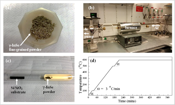
Figure VII.12. (a) Optical image of fine-grained powder of γ-InSe. (b) Tube furnace system used for the growth of In2Se3. (c) The source material and the substrate in the quartz tube. (d) Program profile of the furnace heater.
Download figure:
Standard image High-resolution imageThe β-In2Se3 layers were grown on different substrates such as Si/SiO2, mica and HOPG [1117]. Prior to growth, the Si/SiO2 substrate (7 mm wide and 3 cm long) was cleaned in hot acetone (T = 60 °C) and ultrasonicated in methanol and isopropanol (10 min in each solvent) and then cleaned by oxygen plasma at T = 100 °C for t = 10 min to remove ambient adsorbates from its surface. The cleaned substrate was immediately loaded into the tube furnace for the growth. Mica and graphite were cleaved prior to growth and the fresh surface was used as substrate.
A tube furnace system was used to grow the In2Se3 layers (figure VII.12(b)). The system comprised a Carbolite furnace, a 1 m long quartz tube, a rotary pump and an Ar flow controller (Hastings mass flow controller). γ-InSe powder (~300 mg) was loaded into a ceramic boat and placed at the center of the tube furnace. The substrate was placed in the downstream side 6–10 cm away from the source material, see figure VII.12(c). The pressure was lowered ~ 6 × 10⁻³ mbar using the rotary pump. Then an Ar gas was intoduced at a rate of 150 sccm for 2 h providing P = 1.6 mbar. Thereafter, the system was heated from T = 22 to 600 °C at a rate of 3 °C per minute and kept at 600 °C for 6 h or longer (up to 9 h), see figure VII.12(d). The vaporized In- and Se-atoms were carried by the Ar gas and deposited on the substrate. The system was then allowed to cool naturally to RT. Typically, the source material can be reused for a second cycle of growth.
Figures VII.13(a)–(c) show the as-grown β-In2Se3 layers on Si/SiO2, mica and graphite, respectively. The growth on Si/SiO2 substrates produces near-circular, slightly facetted films with lateral size between 1 and 15 µm (figure VII.13(a)), while highly facetted hexagonal films with lateral size ~100 µm grew on mica, see figure VII.13(b). On graphite, films with arbitrary shape grew (figure VII.13(c)) with preferential growth at step edge bunches on the substrate. The thickness, t, was measured by AFM. It ranges from hundreds of nanometers down to 2.8 nm on Si/SiO2.
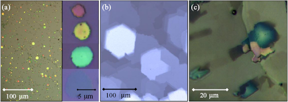
Figure VII.13. Optical micrographs of β-In2Se3 layers grown on (a) SiO2/Si, (b) mica, and (c) graphite (T = 600 °C, t = 9 h and Ar flow rate ~150 sccm). Different colors correspond to different thicknesses of the layers. This ranges from hundreds of nanometers down to 2.8 nm. Adapted from [1117], © IOP Publishing Ltd.
Download figure:
Standard image High-resolution imageFor the same growth conditions (T = 600 °C, t = 9 h and Ar flow = 150 sccm) β-In2Se3 layers were grown on mica with layer thickness between 80 and 5 nm and on graphite from hundreds nanometer down to 10 nm, (see figure VII.13(c)). Figures VII.14(a)–(c) show some examples of growth under different conditions. 'Hay'-like growth was obtained on mica at T = 620 °C for t = 9 h for an Ar flow of 150 sccm, see figure VII.14(a). Nano rods were grown on mica and Si/SiO2, respectively, at 570 °C or under 170 sccm Ar flow rates (figures VII.14(b) and (c)). The growth of different polytype phases of In-Se is highly dependent on the growth T [1114]. This results in a significant advantage of this method since, due to the T gradient within the tube furnace, it is possible to grow different phases and stoichiometries, including γ-InSe, during a single run [1120].
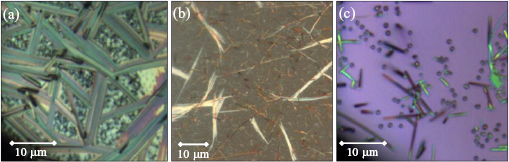
Figure VII.14. Optical micrographs of β-In2Se3 rods (a) grown on mica at T = 620 °C for t = 9 h under an Ar flow rate of 150 sccm, (b) grown on mica at T = 570 °C for t = 6 h under an Ar flow rate of 150 sccm, and (c) grown on Si/SiO2 at T = 600 °C for t = 6 h under an Ar flow rate of 170 sccm.
Download figure:
Standard image High-resolution imageThe electronic and vibrational properties of the as-grown films of different t were compared with those of thin α-In2Se3 and γ-InSe layers exfoliated with adhesive tape from Bridgman-grown ingots [1125, 1126]. The α- and β-phases of In2Se3 are characterized by distinct Raman modes [1117, 1120, 1121]. For the as-grown β-In2Se3 films, the Raman peaks are centered at ~110, 175, and 205 cm−1 at T = 300 K (figure VII.15(a)), corresponding to the intralayer vibrational A1-modes (110 and 205 cm−1) and the Eg-mode (175 cm−1) of bulk β-In2Se3 [1118, 1127]. For exfoliated flakes of α-In2Se3 the Raman modes are narrower and centered at ~104, 181, and 200 cm−1 at T = 300 K. β-In2Se3 flakes exhibit RT PL. RT normalized PL spectra of as-grown β-In2Se3 with t ~ 50 nm are compared with bulk α-In2Se3 and γ-InSe in figure VII.15(b). The PL emission for the β-In2Se3 films is peaked at higher energy compared to α-In2Se3 and γ-InSe, and it blue-shifts with decreasing layer thickness (inset of figure VII.15(c)).
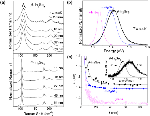
Figure VII.15. (a) Normalized Raman spectra of as-grown β-In2Se3 layers (top) and exfoliated flakes of α-In2Se3 (bottom) at T = 300 K (P = 0.1 mW and λ = 633 nm). (b) Normalized µPL spectra of bulk γ-InSe, β-In2Se3 and α-In2Se3 at T = 300 K (λ = 633 nm and P = 0.1 mW). (c) Measured and calculated dependence of the peak energy, E, of the PL emission on layer thickness t of as-grown β-In2Se3 (black dots) and exfoliated Bridgman-grown α-In2Se3 (blue dots) and γ-InSe (magenta dots) flakes. Inset: Normalized PL spectra of β-In2Se3 with t ~ 50 nm and 6 nm at T = 300 K. Adapted from [1117], © IOP Publishing Ltd.
Download figure:
Standard image High-resolution imageFigure VII.15(c) shows the dependence of the PL peak energy, E, at RT on t, as obtained from several PL and AFM studies of as-grown β-In2Se3 layers (black dots) and α-In2Se3 and γ-InSe flakes [1124] exfoliated from Bridgman-grown crystals [1117, 1125] (blue and magenta dots). The PL peak energy undergoes a blue-shift to higher photon energies with decreasing layer thickness consistent with quantum confinement of photo-excited carriers along the c-axis [1117]. This energy shift can be modelled by a quantum well potential of infinite height, i.e.  where
where  is the band gap for the bulk and
  is the electron–hole reduced mass for motion along the c-axis. For β-In2Se3, the best fit to the measured E versus t, gives
  = 0.04 me and
  1.428 eV, where me is the electron mass in vacuum. These values differ from α-In2Se3, i.e.
  = 0.08me and
  1.390 eV, and γ-InSe, i.e.
  = 0.05me and
  1.250 eV.
The comparison of the PL peak energies for the β-In2Se3 layers with those for α-In2Se3, and γ-InSe [1116, 1119, 1124] indicates distinct spectral ranges for these In-Se compounds and a wider spectral tunability for β-In2Se3 and γ-InSe, among the largest within the wide family of LMs. The larger quantum shift and lighter electron–hole reduced mass for the β-phase compared to the α-phase are assigned to the closer spacing of the layers in the β-phase (Δc/c ~ −1.5%) (figure VII.11), leading to a stronger inter-layer coupling. On the other hand, the larger value of  in β-In2Se3 compared to α-In2Se3 cannot be accounted for by a simple argument and may involve a redistribution of electronic charge between the Se- and In-atoms in neighboring vdW layers [1114]. This may be also affected by the presence of crystal defects, such as In- and Se-vacancies (VIn and VSe), which tend to form in In2Se3 due to the misvalency between the III- and VI-atoms [1114]. Vacancy ordering and bond relaxation due to vacancies are expected to modify atomic orbitals and increase the band gap of bulk layers [1128], and may play a more important role in LMs [1129].
VII.2.3. CVD growth
As is the case with graphene, CVD of LMs is a synthesis route which offers a compromise between film quality and large area coverage and uses techniques compatible with CMOS processing. CVD of LMs other than graphene typically requires two precursor materials which adds to the complexity of depositing uniform, 1L films. Precursors can be sourced as solids which sublime under heating with these vapours then reacting to complete the CVD process, or as gaseous. Gaseous precursors allow much greater control of parameters, such as flow rate, but are often toxic or highly flammable, such as H2S and H2Se [1008].
VII.2.4. Solid precursors
Figure VII.16 describes the microreactor set-up for CVD of MoS2 in which flakes of MoO3 and S powder are used as solid precursors to supply Mo and S, respectively. LPE MoO3 flakes in IPA were drop-cast on a SiO2 chip placed face-down on top. This assembly was heated to 750 °C in a quartz tube furnace under Ar flow (150 sccm) with S powder heated to 120 °C in a separate heating zone upstream of the microreactor. The samples were exposed to the resulting S vapour for 20 min before annealing at 750 °C under just Ar flow (150 sccm) for a further 20 min.
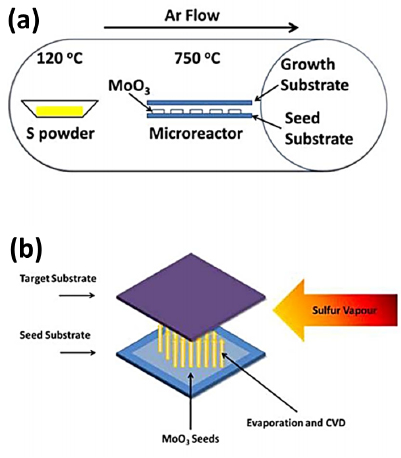
Figure VII.16. (a) Schematic set-up for CVD of MoS2. (b) mechanism by which MoS2 is deposited on the target substrate. Adapted from [1098] CC BY 4.0.
Download figure:
Standard image High-resolution imageImaging of the resultant deposit shows a film consisting of single crystal domains joined together to form a continuous film (figure VII.17(a)). Raman spectroscopy shows the  and E' peaks characteristic of MoS2 [1098] (Figure VII.17(b)), while the spectral contributions to the Mo 3d region of the XPS spectrum are consistent with that of MoS2 with a small amount of oxide present [1098] (Figure VII.17(c)). The
  to E' peak separation ~18 cm−1 and the strong PL (Figure VII.17(d)) are evidence for 1L-MoS2 [1098].

Figure VII.17. (a) SEM image showing continuous MoS2 film. Scale bar is 2 µm. (b) Average Raman spectrum measured across a 20 × 20 µm area of the film. (c) Mo 3d core level showing contributions consistent with MoS2. (d) PL measured across a 1L region (green) and 2L island (pink). Adapted from [1098].
Download figure:
Standard image High-resolution imageCVD of MoS2 on c-plane sapphire using solid inorganic precursors [1130–1132] has enabled an efficient route toward producing high quality 1L-MoS2 films with lateral dimensions (>cm2) beyond that of the mechanically exfoliated flakes (less than 100 µm) with electronic properties matching those of mechanically exfoliated samples [1133].
However, solid precursors such as S and MoO3 exhibit negligible vapor pressure at RT. This leads to the requirement of positioning the precursors inside the heated zone of the reaction chamber to reach T usually above 200 °C for S and 500 °C for MoO3 with fixed distances from the position of the substrates as shown in figure VII.18 with unseeded or seeded substrates. Since the available composition of the precursors in the atmosphere of the reaction chamber depends on the evaporation from the time-dependent masses and surface areas of the solid precursors, it is challenging to consistently control the flow of the precursor vapours reaching the substrates over the period that affects the uniformity and stoichiometry of the resulting film. There is also a practical issue of over-consumption of the precursor materials that may lead to unwanted deposition of residual by-products on the substrates and walls of the reaction chamber which also hinders the growth uniformity and technological feasibility.

Figure VII.18. (a) CVD setup for deposition of 1L MoS2 using solid precursors, MoO3 and S. (b) MoS2 deposited on c-plane sapphire. (c) 1L-MoS2 covering c-plane sapphire without complete coverage, scale bar is 20 µm. (d) 1L MoS2 with complete coverage, bar is 10 µm. Adapted from [1130], copyright American Chemical Society.
Download figure:
Standard image High-resolution imageVII.2.5. Gas precursors
In order to achieve a better control over the gas phase composition of the precursors in the chamber, gas sources with high RT vapor pressures (>0.1 mbar) can be used, which allow the precursors to be stored in a T-and pressure-controlled bubbler, outside the heated zoned of the reaction chamber where the vapour pressure and mass flow rate can be controlled independently, see figures VII.19 and VII.20.

Figure VII.19. Equilibrium vapor pressure of Mo(CO)6 as a function of T based on the measured thermodynamic constants in Ref. [1134].
Download figure:
Standard image High-resolution image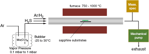
Figure VII.20. MOCVD setup, with a reverse bubbler configuration for Mo(CO)6.
Download figure:
Standard image High-resolution imageA large range of gas precursors containing Mo and S were developed for semiconductor and catalyst industries. They include Mo(CO)6 [1135], MoCl5 [1136], (NH4)2MoS4 [1137] for molybdenum and H2S [1136], diethyl sulphide [1138] for S. Often these techniques using gas precursors are named Metal organic CVD, MOCVD, even if the precursors cannot be considered proper metal organics.
Significant progress has been made using MOCVD in the growth of large-area, reproducible, high-quality TMDs. However, we still have to overcome the challenge of single crystal continuous film growth of MoS2 by MOCVD in a reasonable growth time (~1 h). Basic nucleation and growth processes will have to be developed and understood in more detail before this problem can be solved. More work needs to be done on understanding the basic growth mechanisms which may include in situ growth observations to determine the kinetics and rate limiting steps for systematic MOCVD control of film morphology and micro-nanostructures. Ref. [1139] reported the diffusion-controlled growth of WSe2 on sapphire, where a two-step process was used to nucleate WSe2 followed by growth from the seeds using process conditions to minimize additional nuclei while growing single layers. This is an example of many growth studies that need to be performed in order to achieve large area single-crystal TMDs. While this study has shed some light on WSe2 growth process, single 1L crystals across the whole wafer have not been achieved yet. Another growth process that could be used is atomic layer epitaxy, however at this time there does seem to be a significant effort in this direction, perhaps because a proper substrate has not been identified yet.
So far, the growth of 1L-MoS2 by MOCVD was demonstrated by a few groups with a varying degree of coverage, crystallinity, thickness uniformity, and scalability. Ref. [1140] developed a method to grow a wafer scale polycrystalline 1L-MoS2 films on SiO2/Si with Mo(CO)6 and (C2H5)2S (Diethyl sulfide; DES) with relatively low growth T (~550 °C), albeit with a rather long growth time to achieve a continuous film (~26 h) in low vacuum conditions (7.5 Torr). Ref. [1141] produced average-thickness controlled MoS2 1L-to-ML on cm scale SiO2/Si and sapphire after a thermodynamic modelling of vapor phase equilibrium reaction of the precursors Mo(CO)6 and H2S. The growth pressure (~1 atm to 1 Torr) and T (400 –850 °C) were considered as a main factor in determining the range of growth parameters for the synthesis of high quality MoS2 films of a good stoichiometry without any carbon residues originating from the carbon-containing Mo precursor.
Mo(CO)6 and H2S were used in Ref. [1142] as model precursors. The choice was based on the fact that both are readily available, well-established high purity (>99.9%) MOCVD sources with know thermochemical properties [1141, 1143–1147].
In designing how the sources are delivered, a solid precursor such as Mo(CO)6 is to be loaded into an inert, stainless-steel bubbler immersed inside a T controlled bath. Ideally, the evaporation of Mo(CO)6 is considered to be fast enough to always completely saturate the bubbler with equilibrium vapor pressure (figure VII.19) which would determine the concentration of the precursor exiting the bubbler with the carrier gas. However, the common problem with solid precursors is that the actual vapor transported out of the bubbler quickly decreases over multiple growth runs because of increased dead volume of the precursor and decrease in the available precursor surface area for an efficient evaporation (at least ~1 µl (min · g)−1). In order to tackle this issue, a reverse bubbler configuration (see figure VII.20) and packing of precursor with an inert silica beads ~2 mm are used to increase effective dwell time of the carrier gas and the precursor surface area [1148] by an order of magnitude. These approaches have been previously employed for solid metalorganic precursors to ensure efficient evaporation [1148]. The evaporation rate of the Mo(CO)6 precursor should now be fast (at least ~1 µl (min · g)−1) enough to assume an instantaneous phase equilibrium between gas and solid phases of Mo(CO)6 within the bubbler while the Mo(CO)6 precursor vapour is carried into the reaction zone of the system by an inert gas (specifically Ar). In this case, the partial pressure of Mo(CO)6 exiting the bubbler can be estimated by the vapour pressure of Mo(CO)6 at the T of the bubbler (Tb). Tb is preferably kept below the RT to prevent unwanted condensation of the precursor material upstream, before reaching the heated zone. Typically, a bubbler equipped with a chiller can reach a minimum bubbler T~–30 °C.
The actual amount of Mo(CO)6 introduced to the reaction chamber can be monitored by mass spectroscopy of the atmosphere inside the chamber. Although calibration of the absolute concentration of the precursor is somewhat challenging, the relative concentration can be obtained for every run of the experiment serving as an indicator for the amount of the precursor remaining in the bubbler. At the outlet of the bubbler, in order to abruptly turn on and off the flow of Mo(CO)6, a solenoid valve was installed, which can be automatically controlled, so that the precursor mass flow from the beginning to the end of the MOCVD growth cycle is timed precisely.
As for the S source, mass flow control is more straight-forward as H2S is in gaseous state at ambient conditions and high purity (99.999%) gas can be provided readily from commercially available compressed gas cylinders. However, extreme caution should be exercised since the H2S gas is a highly flammable and toxic gas with an acceptable exposure limit of 20 ppm (set by the Agency for Toxic Substances and Disease Registry, USA). In this regard, H2S gas level detectors both in the ventilated gas cabinet storing the H2S gas cylinder and near the CVD furnace are installed. They are connected to a sound alarm to alert the appropriate emergency services immediately. In addition, experiments thorough He leak test of the assembled CVD system need to the conducted before performing the experiments involving H2S to prevent anyone in the work area from exposure.
The CVD system used, as illustrated in figure VII.20, consists of a horizontal hot wall filament three-zone, quartz tube system (Carbolite HZS 12/-/600) commonly used for laboratory scale CVD synthesis as one of the most economical ways to produce cm scale thin films. The quartz tube is coupled to KF-standard (DIN 28403, ISO 2861) high-vacuum compatible flanges which can be evacuated by a mechanical pump to ~10−3 mbar. All the gas lines are made of stainless connections that prevent any outgassing and extraneous chemical reactions. The size of the sample is limited by the diameter of the tube and length of the heating zone.
MOCVD MoS2 was deposited onto single crystal c-plane sapphire substrates pre-annealed in air at 1000 °C for 1 h to yield atomically flat terraces [1130]. This substrate has yielded much better growth morphology than other amorphous substrates, such as SiO2/Si. The presence of an atomically flat surface is likely to be one of the prerequisites layer-by-layer epitaxy of LMs [1130, 1149, 1150]. Typically, c-plane sapphire substrates are cut into square pieces of 1 by 1 cm by first scratching them with a diamond tipped pen and snapping them into separate pieces by hand. Before the pre-annealing procedure at 1000 °C in air, they are subsequently cleaned in the IPA, acetone, and DI bathes inside a bath sonicator for at least 10 min.
Ref. [1141] computed the thermodynamic 'map' of all possible phases resulting from the vapor reactions for different compositions of Mo(CO)6:H2S:H2, T, and pressures. They found a set of growth parameters with a high growth T ~850 °C, presence of H2(99%), and high growth pressure ~1 atm leading to a good morphology with a large 1L domain size >1 µm and stoichiometry predicted from the equilibrium thermodynamic modelling of the vapor phase. However, vapour phase reactions may not translate very well to what takes place at the substrate surface level, as the non-equilibrium dynamics, mass-transport, presence of boundary layers due to the fluid dynamic condition, and surface reactivity also play an important role in the final surface mediated growth mechanism [171, 765, 1151].
E.g. excessive vapour phase reactions must be avoided, as they may lead to a significant formation of MoS2 particles rather than substrate assisted epitaxy of atomically thin layers [1152–1155]. In order to enhance the heterogeneous, surface reaction over the vapour phase ones, generally speaking, higher T (>800 °C) and pressure (>850 Torr) are preferred [1151].
H2 during MOCVD is used as a reducing agent to prevent the oxidation of MoS2 and deposition of carbon based species. However, H2 is detrimental to the grain size, as the nucleation concentration could increase by an order of magnitude increasing H2 [1140]. Performing the growth at high T, low vacuum environment (~800 °C and 10 mbar) in the presence of H2 would lead to Si contamination of substrate hindering the growth.
In turn, the growth conditions based on Ref. [1141] were used for initial growth studies. The saturated vapour of Mo(CO)6 at the bubbler T~30 °C was introduced into the CVD system (a quartz tube three-zone hot-wall furnace) through Ar carrier gas. c-plane (1 0 0 0) monocrystalline sapphire substrates were placed in the center of the furnace by loading them onto a larger sapphire plate (which serves as a boat) and were heated to the growth T (750 °C–1000 °C) and annealed for 15 min in Ar (75 sccm), followed by added flow of the S precursor, H2S (1.5–20 sccm), before introducing Mo(CO)6 to initiate the MoS2 growth in the S rich conditions that prevent the creation of vacancies due to S removal within the as-grown MoS2. At the end of the growth (typical growth time ~30 min), the Mo(CO)6 flow was shut-off by a solenoid valve and the sample was cooled naturally to RT with Ar and H2S gases still flowing through the quartz tube. All the stages of the MOCVD growth were performed under atmospheric pressure.
After each growth run, the inner wall of the quartz tube was rinsed with DI water and IPA and blow-dried with N2. Afterwards, it was annealed at 1100 °C in Ar (100 sccm) for 2 h and in air for 2 h order to eliminate all the residual precursor and by-product materials.
In order to optimize the growth morphology toward large lateral size (>1 µm) and crystalline 1L-MoS2, the growth parameter space was explored. The T dependent growth of MoS2 on sapphire in figure VII.21 shows the AFM height images of for the conditions that yield low overall coverage without merging of individual nuclei. The MoS2 nuclei form randomly over the surface.

Figure VII.21. Dependent growth morphology illustrated by AFM height images of as-grown MoS2 on sapphire samples produced at different using Mo(CO)6 and H2S as model precursors. Scale bar, 250 nm. Adapted from [1142], copyright American Chemical Society.
Download figure:
Standard image High-resolution imageThe nucleation concentration exponentially decreases with increasing temperature in an Arrhenius fashion (figure VII.22). This is consistent with a surface-mediated process, where the apparent activation energy is linked with various activated surface reactions such as adsorption, attachment, and diffusion [793, 1156].
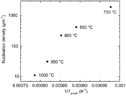
Figure VII.22. Nucleation density versus 1/T for the samples in figure VII.11. Adapted from [1142], copyright American Chemical Society.
Download figure:
Standard image High-resolution imageRaman and absorption spectroscopy (figure VII.23) demonstrate the high optical quality of the as-grown 1L-MoS2, comparable to exfoliated and CVD deposited MoS2 [1130]. E.g. the A, B, C, and D excitonic peaks are visible [1130, 1142], a clear optical signature of MoS2. Moreover, the wavenumber difference between the two prominent Raman peaks, relating to E' and A1' modes is ~19.7 cm−1, close to the standard value of 1L- MoS2. Nevertheless, the grain sizes even for high growth T (1000 °C) are less than hundreds of nm for these growth conditions. This makes further characterization of individual flakes difficult and the polycrystallinity of the film may lead to a significant degradation and non-uniformity in electronic quality for wafer-scale applications.
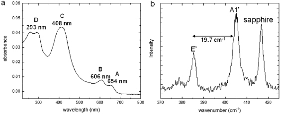
Figure VII.23. (a) Optical absorption and (b) Raman spectra at 532nm from 1L-MoS2 grown at 950° C. Adapted from [1142], copyright American Chemical Society.
Download figure:
Standard image High-resolution imageThe effect of partial and overall pressures of the gas species, Mo(CO)6:H2S:H2 on grain size was investigated. Using XPS, it was found that for low growth pressure (10 mbar or below), the MoS2 film becomes contaminated with Si (figure VII.24) likely originating from the quartz tube, with the reducing environment originating from H2 in the carrier gas and from the decomposition of H2S, not ideal for a clean, growth of 1L-MoS2. In addition, larger amounts of Mo(CO)6 compared to H2 tend to yield bulk particles of non-sulphurized, Mo oxides as probed by XPS (figure VII.25).
Figure VII.24. XPS survey spectra of MoS2/sapphire samples from the two growth runs with different chamber pressures (1 atm and 8.5 mbar). XPS measurements were performed with PHI Versaprobe II equipped with x-ray source, Al Kα; hv = 1486.6 eV.
Download figure:
Standard image High-resolution image
Figure VII.25. Influence of Mo(CO)6:H2S flow rate ratio on MoS2 film composition. (a) and (b) Optical images of two different Mo(CO)6 Ar carrier and H2S mass flow rates of (a) 15 (Mo(CO)6 flow rate of 0.0053 sccm) and 15 sccm, and (b) 5 (Mo(CO)6 flow rate of 0.0018 sccm) and 20 sccm with growth T~ 950 °C, bubbler T~ 30 °C, H2 ~10 sccm, growth pressure ~1 atm, and growth time ~30 min. Scale bar, 25 µm. (c) and (d) Mo 3d and S 2s core-level XPS spectra for the corresponding growth conditions of (a) and (b). (f) S 2p core-level XPS spectra for the corresponding growth conditions of (a) and (b). XPS measurements were performed with PHI Versaprobe II equipped with a Al Kα x-ray source; hv = 1486.6 eV.
Download figure:
Standard image High-resolution imageFigures VII.25(a) and (b) showoptical microscopy images of MoS2 films grown on sapphire, for two different Mo(CO)6:H2S ratios, 4:1 and 1:1 respectively. The core-level XPS spectra of Mo 3d, S 2s, and S 2p demonstrate that the low Mo(CO)6:H2S condition provides a good stoichiometric film of MoS2 with only small (<1%) amount Mo in different chemical state (Mo5+) than MoS2 (Mo4+), while the high Mo(CO)6:H2S condition leads to undesired deposition of thick Mo particles likely oxidized in 5+ state, with a poor Mo:S stoichiometry consistent with the thermochemistry of the Mo, O, S, H system [1147].
VII.2.6. Reduction of the nucleation density using alkali metal halides
So far MOCVD has produced 1L-MoS2 with average domain size <1 µm[1157, 1158]. This presents a challenge towards production of single-crystal 1L-MoS2 over the length scale of the substrates. In order to improve the domain size, one could employ alkali metal halide salts such as NaCl, KI, and KBr. The use of thes salts was documented in MOCVD experiments to improve domain sizes, involving precursor combinations of Mo(CO)6 and (C2H5)2S [1140], MoCl5, and (CH3)2S, [1159] and conventional CVD [1160] on SiO2/Si. A metal halide, such as NaCl or KI powders (~0.01–1 mg), was placed in the upstream area of the furnace either in a boat or plate of alumina [1142]. Mo(CO)6 was introduced at ~600 °C for 30 min before introducing H2S at higher T (750 °C–1050 °C). A nucleation suppression effect is observed [1140], where 1L-flakes > 10 µm can be achieved. Analysis by optical absorption, Raman, PL spectroscopy and XPS in figure VII.26 indicate that this MoS2 exhibits a direct-band gap without significant defects, strain, impurities and doping comparable to those of 1L-MoS2 grown by conventional CVD. Furthermore, the crystal facets are highly aligned in one direction, demonstrating a successful lattice-orientation matched epitaxial deposition of MoS2 on single-crystal sapphire. T dependent field-effect transistor characterization using polymer electrolyte gating demonstrated a promising n-type µ~100 cm2 V−1 s−1, similar to 1L-MoS2 deposited by conventional CVD [1149].
Figure VII.26. (a) Optical microscopy of 1L-MoS2 with NaCl placed upstream. Scale bar: 25 µm. (b) Raman spectroscopy on a single crystalline 1L-MoS2 area (c) optical absorbance. (d) PL spectra from single crystalline 1L-MoS2 flake as-grown on sapphire and transferred onto SiO2/Si. Adapted from [1142], copyright American Chemical Society.
Download figure:
Standard image High-resolution imageIt is currently not clear exactly how the domain enlargement or the suppression of nucleation by the metal halides occurs. The desiccating effect of NaCl salt as suggested by Ref. [1140] is not likely to be the dominant factor since even a very small amount of salt (<10 µg) could be used, where it would decompose before the growth reaction. Ref. [1159] suggested that salt helps to reduce the carbon contaminant, which might hinder crystallization, from organic parts of the MOCVD precursor. Refs. [1161, 1162] suggested that the presence of alkali metals leads to decrease in the melting point of oxide-based Mo precursors and even the melting point of a substrate [1163], increasing the reactivity. This in turn could lead to the increased diffusion and reduction in the nucleation density. Na oxides or compounds of sodium and molybdenum oxides (NaxMoyOz) [1160, 1162, 1164] may also play a role, as they were found at the interface between as-grown 1L-MoS2 and substrate [1164]. It was also found that after growth, where the salt was initially present, the halogen atoms evaporated away from the substrate surface while the alkali metals remained [1142]. Na2MoO4 alone (without any halogens) is effective precursor for growth of large domain sizes [1165]. Large area MoS2 growth of large domain sizes was acieved on Na doped glass substrates [1164, 1167]. Na especially impacts the growth of large crystalline domains at a wide range of growth T (720–1050 C). The exact role of the alkali metals remains to be investigated, as there are numerous competing atomistic processes, such as surface diffusion, nucleation site activation, attachment kinetics that control nucleation and growth, which all can influence the nucleation density and domain size.
This be extended to perform MOCVD of vertical and horizontal heterostructures of TMDs, such as MoWS2 and MoWSe2, using currently available metalorganic sources, such as W(CO)6, and dimethyl selenide [1168]. In addition, doping of TMDs may also be achieved by introducing dopant precursors, as done for MOCVD of other materials systems [1169, 1170]. Low toxicity, low-cost precursors should also be considered, in order to achieve a safer and more accessible production of TMDs.
VII.2.7. ALD
Atomic layer deposition (ALD) techniques were presented as a modified CVD to produce thin layers of MoS2 using the precursor pairs—MoCl5 and H2S [1171], Mo(CO)6 and H2S [1157], Mo(CO)6, and dimethyl disulphide [1172], Mo(NMe2)4 and 1,2-ethanedithiol [1173], on various insulating substrates such as SiO2/Si, sapphire, and mica. However, often the end products are misaligned nanocrystalline MoS2, with varying degree of thickness likely resulting from the low growth T ~300 – 600 °C). Although it is more challenging to prepare and control the stoichiometry of the product, MOCVD of MoS2 using single-source precursors, tetrakis(diethyl-dithiocarbamato)molybdenum(IV) [1174] and Mo(S-t-Bu)4 [1175] were also investigated.
7.2.8. Brief comparison methods for the growth 2D semiconductors
In the table VII.2, we summarize the methods for the growth of LM semiconductors presented in this chapter.
Table VII.2. Basic conditions for growth of TMDs.
| Method | Material | Substrate | Precursors | Temperature | Pressure | Reference |
|---|---|---|---|---|---|---|
| CVD | MoS2 | SiO2 | MoO3 and S | 750 °C | Atmospheric | [1008] |
| MOCVD | MoS2 | Sapphire | Mo(CO)6 and H2S | 600 °C–700 °C | Atmospheric | [1142] |
| TAC | MoS2, WS2 | Quartz, SiO2 | Mo, W, S | 750 °C | Atmospheric | [1093] |
| PVT | β-In2Se3 | SiO2, mica, graphite | γ-InSe | 600 °C | 1.6 mbar | [1117] |
VII.3. Layered materials heterostructures
Typically, heterostructures of semiconductor compounds have been fabricated using isostructural substrates with nearly lattice matched substrates. One of the advantages of LMs is that the lattice matching requirements needed for cubic materials systems is relaxed [1149]. Lateral heterostructures are also a focus of research [1176]. Growth of lateral and vertical heterostructure could enable a number of devices [1177]. Many groups have fabricated and studied aligned and unaligned LMHs with the objective of making new devices and scale transistors beyond the CMOS limit [1178–1183]. Many of these LMHs were fabricated using exfoliation and transfer rather than direct growth. It would be desirable to use CVD to fabricate them. In the case of h-BN and graphene, because of their refractory nature, a catalyst is used to grow them. HBN or graphene would be ideal substrates for other LMs. Thanks to its atomically flat surface, low interlayer electronic coupling and almost perfect reticular matching, h-BN is an ideal substrate for graphene [1184]. Many of the researched LMH devices also include TMD semiconductors [112, 1185]. However, these materials have challenges of their own as discussed in section VII.2 In order to create LMHs containing semiconducting TMDsor BLG, metals (TMD and graphene), and dielectrics (h-BN), a significant amount of effort is needed either via repeated transfer of the individual LMs or direct growth [1177].
LMHs of cubic systems were grown by MBE and CVD, MBE being the work horse for bulk III-V heterostructures today. Both CVD and MBE were used for the growth of TMDs [1186–1189] while CVD [765, 1038] has advantages for graphene [765, 1038] and h-BN [836, 1054, 1055, 1087, 1190, 1191]. CVD may be the most suitable technique for the scalable synthesis of highly-crystalline LMHs even though the selection of the final deposition equipment and preferred precursor types have not been finalized yet. Such CVD approach is not trivial as weak interlayer interactions favor 3d island growth [1192]. The formation of multi-layer islands is typically avoided by using high chalcogenide to metal ratios adopting short reaction times, which leads, however, to isolated crystals [1192–1196]. Growth LMHs, vertical or lateral, is challenging. In this section we will discuss a few materials options[1192].
There are several reports targeting the Controlled lateral and vertical TMDs heterostructure growth [1197–1199]. Controlled grown of lateral heterostructures of TMDs would enable quantum engineered devices, through band alignments, enabling new generation of electronic devices [1177, 1200]. 1L-TMDs can be grown sequentially to construct in-plane LMHs, otherwise not achievable through other processes such as transfer of grown or exfoliated films. Ref. [1200] demonstrated a direct synthesis of lateral LMHs of MoS2 − WS2 and MoSe2 − WSe2 by using ambient-pressure CVD with aromatic molecules as seeding promoters. Vertical LMHs, while simpler, will require significant effort is reducing 3d growth [1201, 1202].
VII.3.1. Graphene/h-BN stacks
There are several types of LMHs that can be envisioned for future devices: (1) vertical, (2) lateral, (3) twisted (controlled and uncontrolled). Graphene and h-BN have been grown by a number of catalytic CVD [1203, 1204] and plasma enhanced techniques [963]. Catalyst-free graphene growth yields poor crystal shapes and crystallinity, with low rates [947, 1204, 1205]. Ref. [836] used a catalyst-free CVD approach to synthetize crystalline graphene on exfoliated h-BN, with noticeable growth rates on single-crystal on-axis SiC substrates (either Si- or C-face). SiC was selected because of its high thermal stability [1206], in view of the high growth T, typically >1200 °C, needed for a non-catalytic growth approach. The SiC(0 0 0 1) samples were diced from commercially available wafers and then cleaned via wet chemistry, prior to mechanical exfoliation of h-BN. They were immersed in an ultrasonic bath of acetone and then IPA for 3 min each followed by a DI water. They were then cleaned in HF (48% solution) diluted in DI water (1:10 HF: DI-H2O) for 1 min to remove the native oxide and thoroughly rinsed in DI water. The samples were then subjected to an oxygen plasma (O2 flow, 80 W, 5 min) to completely remove the organic or carbonaceous contaminants. The SiC surfaces, which had polishing scratches in the as purchased form, were hydrogen etched in the same vertical cold-wall reactor (Aixtron, HT-BM) for 4 min in an atmosphere of high purity (6N) H2 and Ar at 1230 °C and a total pressure of 450 mbar using 500 sccm flow rate for each gas. AFM was used to measure the SiC surface roughness and only substrates with atomically flat surfaces were used for growth. PDMS stamps were used for mechanical exfoliation of h-BN on the hydrogen etched SiC. To this end, two PDMS stamps with dimension of 2 × 2 cm2 were adopted and the mechanical exfoliation process was repeated more than 40 times. The clean SiC substrate was then pressed on the PDMS stamp for 20s. This process yielded h-BN flakes with lateral size up to 150 µm. The PDMS residue on top of the h-BN/SiC was removed by using first acetone for 3 min and then IPA while gently shaking the beakers. Ultra-sonication was not adopted, since it causes detachment of the mechanically exfoliated h-BN flakes from the SiC substrate. Finally, the samples were treated with a 25 W oxygen plasma for 30 min. This last step was found to be crucial for obtaining single crystal graphene on h-BN as it allows for removal of adventitious carbon contaminations [836]. The h-BN/SiC substrate was then placed in the Aixtron HT-BM system and positioned in the central recess of the heater (see figure VII.27) for subsequent graphene growth.

Figure VII.27. Growth chamber of the Aixtron HT-BM vertical cold-wall reactor used for growth of graphene on h-BN.
Download figure:
Standard image High-resolution imageThe h-BN films on SiC were then annealed in an 8 mbar H2 pressure, with hydrogen flow of 1000 sccm at 1150 °C for 10 min. [836]. Single crystal graphene was then grown under the following conditions: 150 sccm H2, 1000 sccm Ar and 5 sccm of methane (CH4) for 30 min. The H2:CH4 ratio was found to be a critical parameter for the growth of high quality graphene. H2:CH4 ratios of 1:1 yielded polycrystalline graphene with rounded edges, and a ratio of 1:30 yielded hexagonally shaped single-crystal graphene domains. The optimum growth T was found to be 1150 °C. Lower growth rates were achieved at 1000 °C [836], but little to no growth was observed below this T. Above 1150 °C, growth was also achieved, but clustering of amorphous carbon was also often observed [836]. Growth was performed at different pressures ranging from 7 to 150 mbar. This yielded smaller (<0.5 µm) and bigger (>2.0 µm) domains for low and high pressure conditions respectively. Carbonaceous clusters were occasionally observed at the higher pressures (150 mbar). For this reason, the growth pressure should be limited to 25 mbar to prevent the formation of such clusters. Lower hydrogen flows (i.e. 100 sccm) and longer growth times were also be used to obtain continuous films. With hydrogen flows >150 sccm only partial growth of hexagonal single-crystals could be achieved. At the end of the growth process at high T, the system was cooled (300 °C min−1) in the same atmosphere of Ar and H2 used during growth. The sample was unloaded from the chamber for T < 120 °C.
VII.3.2. TMD/h-BN and TMD/grapheneLMHs
There are many reports on growth of sulfides [1196, 1197, 1207–1210] and selenide [1139, 1176, 1211–1213] TMDs using a variety of precursors using similar CVD systems, although this is far from the optimal or desired approach. Direct growth of WS2 on other LMs resulted in isolated grains at the micron scale [1194] or uncontrollable growth of FL-WS2 on graphene [1195] and isolated grains on h-BN [1196]. What is critical in the initial crystal growth process development, in addition to identification of the materials and the equipment and precursor selection and design, is the understanding of nucleation and growth of controlled TMD layers. Some inroads in the basic understanding for both MBE as well as CVD were reported in Refs. [1201, 1202, 1214].
A CVD approach to obtain continuous 1L-WS2 on h-BN and graphene was reported [1209] following similar growth procedure used for MoS2 [1189, 1215]. Ref. [1216] used a similar method to grow MoS2/h-BN LMHs, as well as growing h-BN by CVD as shown in figure VII.28.
Figure VII.28. Schematic of two fabrication processes of MoS2/h-BN LMHs. The first consists in transferring the CVD grown film from a Cu foil to the center of a Si/SiO2 chip, leaving four corners of the substrate to be bare SiO2. This substrate is then loaded face up into the CVD system to grow MoS2 on it. The MoS2 domains will cover both h-BN and SiO2 areas. The second approach is through a two step PMMA assisted process. The CVD grown h-BN film is first transferred onto the center of a SiO2/Si chip, followed by stacking another layer of CVD grown MoS2 on the whole substrate surface, obtaining transferred MoS2 domains on h-BN in the central area. Two of the transferred bundaries of h-BN on the SiO2 surface in the first fabrication method are labeled A and B. Adapted from [1216], copyright American Chemical Society.
Download figure:
Standard image High-resolution imageSulfurization of WO3 powder (Sigma Aldrich, 99.995%), was carried out within a horizontal hot-wall furnace. This is is basically a two-zone system with WO3 within a high T zone, and Sulphur (Sigma Aldrich, 99.99%) in a quartz crucible in a cooler zone, of the furnace as shown in figure VII.29. The system is connected to a scroll pump, which ensures a base vacuum ~5 × 10⁻² mbar. The h-BN and graphene substrates are prepared through MC on either quartz or SiCwith variable (up to 1 cm2) surface area. Quartz substrates are cleaned with a piranha solution (3:1 H2SO4:H2O2) for 15 min and acetone and 2-propanol semiconductor grade for 3 min each before flake exfoliation. SiC substrates are also threated with 5% HF in water for 1 min to remove the SiOx on the surface. After the exfoliation of h-BN, the substrates (either quartz or SiC) are treated with an oxygen plasma (5 min, 80 Watt) to remove possible scotch tape residue.
Figure VII.29. (a) Scheme of the furnace used to grow continuous films of WS2 on graphene and h-BN; (b) picture of the furnace. Adapted from [1217], with permission of The Royal Society of Chemistry.
Download figure:
Standard image High-resolution imageWS2 can also be grown on polycrystalline or single crystal CVD graphene [766, 841] transferred on quartz or SiC cleaned as described above. For WS2 growth on graphene on SiC, fresh as-grown samples are used. Both are cleaned for 3 min in acetone and for 3 min in 2-propanol. Crucibles are cleaned with 2-propanol wet tissue and subsequently annealed in the furnace used for the growth at 1100 °C for 60 min in 200 sccm Ar before each growth. This 'empty run' ensures having both a reactor and clean crucibles. After annealing usually the crucibles are electrostatically charged. This can alter the weighing of the reactants. The electric field interacts with the WO3 powder, which sticks to the crucible and spreads around in a not reproducible way. Hence, the crucible needs to be grounded before weighing.
There are many important details related to oxide powder preparation, loading and placement in the horizontal furnace. The substrate and WO3 are placed in the same flat 1-inch wide crucible, next to each other, but well separated to avoid accidental deposition of the powder on the substrate. The WO3 powder has to be spread uniformly on the quartz crucible after weighing in order to maximize the reaction surface. The distance, typically ~1 cm, between substrate and WO3 powder is also important to control the surface coverage. The S powder is placed outside the hot zone of the oven in the Ar upstream part, ~20 cm away from the furnace (see figure VII.29). A heating belt is wrapped around the tube region where the S is placed to control evaporation. It is important that the growth reaction occurs under S rich conditions. To ensure this, two aspects are crucial:
- 1)S and WO3 powders have to be in a ratio between 50:1 and 100:1. If not, the reaction typically stops at the intermediate step of WO2 cluster formation. Optimum weights ~100 mg of S and 1 mg of WO3 were reported.
- 2)S has to be delivered when WO3 has reached a stable optimal T. To achieve this, this process can be followed. Once crucibles and target sample are in place within the reactor as shown in figure VII.29(b), the growth can start. The ramp-up phase has two steps: (i) ramping up to 350 °C at 10 °C min−1 with no gas flowing to favor sample outgassing; (ii) ramping up to 900 °C (still at 10 °C min−1) while the Ar flow is set at 500 sccm (tube pressure equals 4 mbar) in order to keep the S powder solid. The purity of the Ar gas is 99.9999%. Once the hot zone reaches the working T~ 900 °C, the Ar flow is reduced to 8 sccm (i.e. tube pressure ~0.5 mbar) to ensure S delivery. The heating belt wrapped around the S zone has to be turned on in order to reach 200 °C when the hot zone reaches the working T. This ensures S feeding for ~30 min. The total process is ~1 h long to anneal the surface of the sample after the growth reaction. The sample is then cooled to RT by shutting the power to the furnace and, once 400 °C are reached, the furnace lid is opened to speed up cooling.
VII.3.3. TMD/TMD LMHs
CVD and MOCVD can also be used for growing different types of TMD LMHs [1176, 1198, 1199, 1218]. Lateral LMHs between different TMDs show atomically sharp interfaces with an abrupt transition between constituent materials, without voids and other defects. Using direct growth instead of material transfer has the benefit of a residue-free LMHs and scalability to large areas.
Lateral and also vertical 1L-LMHs both based on the same metal such as MoS2 and MoSe2 [1218], WS2 and WSe2 [1218], as well as different metals, such as WSe2 and MoSe2 [1176], MoS2 and WS2 [1198], MoSe2 and WSe2 [1176], and WSe2 and MoS2 [1199] have reported using CVD based on solid sources. Control over gas flow during the CVD process can also allow the growth of superlattices with well-controlled spatial modulation [1220, 1221].
Some of these materials can be used as lateral p-n junctions without employing in situ doping, as e.g. in the case of MoS2 and WSe2, where the boundary between the two materials serves as a p-n junction [1222] and can be used as a LED. Theory also predicted novel behaviours, such as efficient charge separation [1222] and spin/valley filtering [1223].
While these methods yielded perfectly stacked materials, they are limited to very small lateral dimensions and a few selected material sets. TAC methods are an alternative for large scale production of TMD/TMD heterostacks. TAC opens various avenues for the formations of large scale LMHs as in figure VII.30. Figure VII.30(a)) shows the subsequent deposition of two different metals by PVD followed by TAC. This works for sulfides or selenides of metal in which the conversion takes place at a similar T. The second example in figure VII.30(b) is the growth of a TMD by TAC followed by a second metal deposition and TAC. The third is the large scale mechanical transfer of one TAC film on top of another (figure VII.30(c)
Figure VII.30. Different method used to create TMD LMHs, (a) Co- conversion of both metal films together to form TMDs. (b) Sequential conversion of metal films. (c) LMH formation through stacking pre-converted films.
Download figure:
Standard image High-resolution imageRaman spectroscopy was employed to analyse the interface between the two TAC films in a LMH. It was used to analyse the effect of co-converting the two metal films versus sequentially converting them. This experiment was performed with MoS2 and WS2 as they both can be sulfurised in the same T range, 800 °C. The co-sulphurized sample had both metals sputtered and converted to the equivalent TMD together, while the sequential sample had the Mo deposited and converted, then the W deposited and converted. Shadow masks were used to give the cross structure indicated in figure VII.31(a). Both samples were then Raman mapped, with a spectrum taken every 300 nm over a 10 µm × 10 µm area. All spectra are normalised to the SiO2 peak ~520 cm−1. This data was then used in figures VII.31(d) and (e), which show the frequency position map of the MoS2  peak. For the MoS2 area the peak is at ~383 cm−1 (blue) in both maps. The WS2 and SiO2 areas, with no peak in this frequency region, show only random noise. In the overlap region, for the sequentially sulphurized sample figure VII.31(d), the maximum intensity is very close to the same frequency as the MoS2 area. However, in the co-sulphurized sample figure VII.31(e), there is a noticeable shift to a lower wavenumber as shown by the green colour. This is an indication of increased alloying at the interface in the co-sulphurized sample. A similar effect was seen in Ref. [1224] where they saw increasing shift of the MoS
  to lower wavenumber with increasing alloying with W.
Figure VII.31. (a) Legend for Raman maps. (b) and (c) Raman map of MoS2/WS2 A1g peak position for sequentially and co-converted films. (c) and (d) Raman map of MoS2/WS2  peak position for sequentially and co-converted films. (e) and (f) Raman spectra of MoS2/WS2 for sequentially and co-converted films respectively.
Download figure:
Standard image High-resolution imageTo confirm this, the A1g peaks of MoS2 and WS2 were analysed, position maps are shown in figures VII.31(b) and (c). These peaks are both in the same frequency region ~400–430 cm−1 so to distinguish between changing peak intensities and peaks shifting frequency, these peaks were fitted. What is expected in the case of alloying between the layers is that the A1g peak of MoS2 and WS2 will both shift towards an intermediate value, as observed. For the sequential conversion there is a small shift of both peaks towards each other by ~1 cm−1. For the co-conversion the peaks each shift by ~4 cm−1 towards each other, indicating more alloying in the co-conversion case.
Even though large scale LMH formation by co-conversion was successful [1224], the electrical performance was poor probably due to the roughness of the films and some level of alloying during the TAC process. Co-sulfurisation (figure VII.31(a)) was used to create catalyst for hydrogen evolution, [1225] while the subsequent sulphurization of Mo and W (figure (b)) was employed to create PDs [1226].
VIII. Functionalization of GRMs
A number of strategies have been developed for the functionalization of GRMs. On one hand, this is driven by the curiosity of chemists to master controlled surface modification. On the other hand, functionalization is of great practical importance, as it has the potential to tune the properties according to the needs of specific applications. In this section, an overiew is given in particular focusing on the practical requirements for successful modification of GRMs. A broader overview, is also given in Refs. [160, 165, 1227–1229].
Typically, functionalization is classified as noncovalent or covalent as outlined in Ref. [160] and brifly summarized below. Noncovalent involves the adsorption of other species without covalent bond formation. It is therefore often considered as 'non-destructive', since the lattice is not altered, or referred to as physisorption. However, physisoprtion is not a precise term for noncovalent functionalization. This is because not only van der Waals interactions can occur. Often, more specific, stronger noncovalent interactions are exploited, e.g. dipole and ionic interactions [1771], or π–π stacking, which is specific to graphene with a conjugated sp2 carbon network. The term covalent modification is used when covalent bonds are formed [1329]. Often, this is referred to as chemisorption. For graphene this includes various cases: from new C–C bonds on the basal plane leading to a rehybridization from sp2 to sp3 [1772, 1773], to modifications of defects (e.g. edges [1773–1776]) or the production and derivatization of GO [156, 160, 1799].
In all cases, the properties of the parent material are modified, but in a different way and to a different extent. E.g., the grafting of other species on the surface can be used to form functional architectures or to adjust the compatibility with other materials in composites. Functionalized GRMs typically also display a better dispersibility (higher concentration), especially in solvents that can otherwise not be used. In terms of electronic properties, noncovalent functionalization can be considered as a 'milder approach': while it can be used to controllably dope graphene, it does not harm the conjugated basal plane network and thus does not alter the intrinsic electronic properties dramatically. In turn, covalent functionalization of GRMs essentially creates new materials with distinct properties. E.g., covalent functionalization of graphene is a tool to open a band gap, but at the cost of reducing µ [1780, 1781].
VIII.1. Covalent functionalization of graphene
VIII.1.1. Reductive bulk functionalization
The covalent functionalization of carbon allotropes, especially graphene, is a major research topic in the growing field of functional nanomaterials. The development of novel architectures built-up from graphene requires the availability of a cheap source with low polydispersity. Chemical bulk functionalization of graphene using graphite as starting material has gained significant interest since it allows (i) the generation of exfoliated graphite sheets in large quantities compared to other exfoliation techniques [375, 377, 1230], (ii) access to solution-processable graphene [373, 374], (iii) access to modified physical properties compared to pristine graphite [1231, 1232], and (iv) the investigation of the intrinsic chemical and physical properties of graphane [160, 1230]. Graphite can be activated by reductive charging using an alkai metal, which subsequently leads to a Coulomb driven, solvent-based exfoliation [160, 373, 375], as sketched in figure VIII.1. The intermediately generated material is negatively charged and commonly referred to graphenide [1233]. It can be reoxidized by benzonitrile or other chemical agents [1234], yielding SLG and FLG [375], or trapped by a variety of different electrophiles, yielding covalently functionalized graphene with a variety of functional entities. By this route, hydrogenated [369, 1235, 1236], alkylated [368, 1237–1239] and arylated graphene [370, 1240, 1241] are accessible in a one pot synthesis.
Figure VIII.1. Reductive exfoliation/functionalization of graphite.
Download figure:
Standard image High-resolution imageThe entire functionalization sequence has to be carried out without oxygen and moisture under inert gas atmosphere in a glove box, otherwise a substantial amount of side products is formed [375, 1247, 1242, 1243]. Reductive graphene functionalization represents a versatile protocol which can be applied to graphene in dispersion as well as to SLG on substrates. The latter approach can be used to elucidate topological and mechanistic details of the reaction [1237, 1244].
A variety of experimental conditions are reported in the literature [160, 1777–1779]. From the starting graphite sources, to the composition of the GICs, the employed solvents and/or the used equivalent number of the organic addends, to name a few. We will overview different aspects of fundamental importance for the successful covalent functionalization of graphene, starting from reductively activated bulk graphite: (a) Type of starting graphite, (b) solvents used for the exfoliation, and (c) type of GIC and electrophilic trapping reagent [371, 1238]. Covalently functionalized graphene, without initial reductive activation of graphite, can be accessed by a variety of other synthesis approaches [1245–1247].
VIII.1.1.1. Type of starting graphite
In the context of the reductive graphite exfoliation/functionalization protocol, almost any type of graphite, can be used. A variety of graphite starting materials with different physical and morphological properties were screened [1248] and based on that their covalent functionalization studies focused on 3 types of graphite [1238]: (a) Natural flake graphite (Kropfmühl AG, Passau) with a particle size of 18 µm and a low intrinsic density of defects as expressed by I(D)/I(G) ~ 0.2, with a regular stacking order, (b) PEX 10 (Future Carbon AG)—an expended powder graphite with grain size of ~3–5 µm and I(D)/I(G) ~ 0.3 and, (c) SGN18 (Future Carbon AG)—a spherical, defect-rich graphite with I(D)/I(G) ~ 0.4, with a grain size ~20 µm.
In general, the chemical reactivity of graphite with respect to a reductive covalent functionalization scenario strongly depends on the nature and in particular the morphology of the starting material. It is key that the starting material is dry and free of oxygen. Therefore, a thermal annealing step (300 °C, vacuum, 4–5 d), is used to remove any oxygen inclusion. For materials with intrinsically large graphene basal planes (e.g. natural flake graphites) a reductive charging/exfoliation is very difficult. The intrinsic flake size can be reduced by grinding with NaCl, in particular, the graphite is ground with 5 times the amount of NaCl in a mortar for 20 min. After the elution of NaCl with distilled water and drying in vacuum, smaller and easier dispersible flakes can be obtained.
For the reductive charging/activation of graphite, 4 approaches can be pursued: (a) Electron transfer reagents [1239], (b) Birch-type based reduction [1249–1252] in liquid ammonia with alkali metals [374], (c) reduction with sodium/potassium alloy [1253], and (d) the generation of alkali metal/GICs [373, 1254]. In the latter two cases, the balanced combination of intercalation-driven layer expansion in combination with a Coulomb-repulsion-driven interaction facilitates exfoliation and the wet chemical functionalization of the electronically activated graphene sheets. The solid-state-based graphite intercalation process (d) allows for a fine tuning of the different alkali metal to carbon stoichiometries from KC4 to KC24 [370]. K is used to reduce graphite and to generate the respective GICs. The metal is directly mixed with graphite in an inert gas atmosphere (glove box <0.1 ppm O2, <0.1 ppm H2O) at 150 °C overnight. By changing the alkali metal amount, different intercalation compound stages can be obtained e.g. KC4, KC8, KC16, and KC24. The reductive activation of flakes, deposited on substrates, or CVD SLG can be carried out by applying of a droplet of liquid Na/K alloy (1:3) in 1,2-dimethoxymethane (DME). The deep-blue Na/K alloy solution can be prepared inside a glovebox and stirred for 3 d in an Ar atmosphere. After the graphene activationfollowed by the addition of the trapping electrophile, the remaining reagents can be rinsed off by dry and degassed DME.
The type of graphite activation used prior to the addition of the trapping electrophile has a significant influence on the outcome of the functionalization sequence and the obtained graphene architectures [1235]. The hydrogenation of graphite the GIC (d) yields polyhydrogenated graphene with the highest hydrogen content when alcohols are used as trapping reagents [1235], whereas for the Birch-type reductive activation (b) the highest hydrogen content is obtained for water [369]. This can be explained by the nature of the solvent. In the latter case, ammonia is used at −75 °C and interacts with the trapping water (formation of ammonium hydroxide in an equilibrium reaction). This underlines that the applied reductive activation conditions of graphite have a fundamental influence on the outcome of the reaction.
VIII.1.1.2. Solvent preparation
Water- and oxygen-free solvents are mandatory for the successful exfoliation of the reductively activated graphite starting material and in order to suppress side reactions during the functionalization sequence [375, 1242, 1243]. The solvent has to be stable against the intermediately generated negatively charged graphene sheets (graphenides). The most suitable solvents with respect to these prerequisites are tetrahydrofuran (THF) [1242], 1,2-dimethoxymethane (DME) [1255] and N,N'-dimethylacetamide (DMAc) [1256]. Although widely used for the dispersion of negatively charged CNTs and graphene, DMSO is thought to partially quench the respective negatively charged carbon allotrope, yielding methylated side products [1242, 1256].
Regardless of solvent used, the most crucial step for the wet-chemical reductive functionalization of graphite is the initial solvent purification. Stabilizers, water and/or oxygen traces can influence the reaction outcome and may lead to undesired and uncontrollable side reactions [1242]. Ref. [1257] established a multistep solvent purification protocol using molecular sieve. Ethers (THF, DME) must be stored under light exclusion in order to suppress any auto oxidation processes. The water content of the solvent can be determined by a Karl-Fischer titration. A sufficiently low water content value, THF: < 2 ppm, DME: < 0.5 ppm, allows to proceed with the next solvent treatment step: the removal of oxygen traces by a freeze-pump-thaw degassing. For this purpose, the solvent is transferred into a Schlenk flask and frozen by the aid of liquid nitrogen. The flask is connected to a vacuum line in order to remove the gas phase. Afterwards, the solvent is allowed to warm to RT (gas bubble evolution from the solution). Subsequently, the solvent is frozen again and the gas phase is removed in vacuo (~10−2 mbar). This procedure is iteratively repeated several times (4–6 cycles) until no gas evolution is detected during the thawing process. In order to remove any residual water traces, a distillation over Na/K alloy is carried out. Here, a Na/K alloy (1:3) is freshly prepared and added dropwisely to the solvent. A water separator connected to the distillation apparatus and filled with dried molecular sieves allows additional drying of the solvent. Preferably, the solvent is stored in an Arfilled glove box in order to prevent any further contamination. The purity of the solvent can be checked upon addition of GIC. Here, the bronze color of the GIC must be preserved.
VIII.1.1.3. Type of GIC and electrophilic trapping reagent
Several electrophiles have been utilized in solid support and in homogeneous dispersion functionalization of graphenides, like the diazo coupling [1253], iodonium coupling [1240, 1258], alkylation [368, 1237–1239], arylation [370, 1241], hydrogenation [369, 1235, 1236], halogenation [1259], and silylation [1255]. In addition, by an iterative repetition of the charging/functionalization step, mixed functionalized graphene derivatives are accessible [1244]. However, there is a huge dispersion of the experimental conditions in literature [368, 1239, 1258, 1777, 1778]. In this sense, a complete study surveying all the reaction parameters and determining the most effective synthetic routes is highly desired. Even more important, a deeper understanding of the correlation between bulk approaches, aiming at functionalized SLG and direct functionalization is of utmost interest [368, 370, 371, 1227, 1238, 1253]. Ref. [371] compared 3 reductive functionalization pathways (phenyldiazonium- and bis-(phenyl)-iodonium salts as well as aryliodide) and the reductive alkylation route using hexyl- and dodecyliodide. The use of iodide derivatives with spherical graphite as starting materials is the most efficient to achieve functionalized materials. A single electron transfer (SET) process from the charged graphenides towards the electrophilic trapping reagent can be expected as the primary reaction step. This leads to the generation of radicals in the proximity of the graphene sheet, with subsequent covalent bond formation [1260, 1261]. In this line, the diazonium/iodonium coupling reactions are more expedite than the alkylation, because the generated phenyl radicals are significantly less stable than the alkyl ones due to the much higher bond strength of aromatic C–H bonds [1262]. This higher stability, as well as improved solubility, of the resulting functionalized graphene in DME, plays the major role during the functionalization process, favoring the reaction of hexyliodide with new graphenide activated surfaces, leading to higher functionalization and explaining the narrow Raman I(D)/I(G) distributions [371]. In contrast, faster reactions (i.e. diazonium) lead to broader distributions, probably related with a clustering of the functionalities [371]. The open question regarding the role of remaining negative charges after the initial electrophile addition step was also addressed [1242]. According to Ref. [371] the role of the remaining negative charges can be neglected. This is in contrast to unfunctionalized graphenides. The exposure of these air-sensitive intermediates towards air, leads to a covalent framework modification with an attachment of OH- and H- groups [375, 1243].
Refs. [368–374] demonstrated that GICs are suitable for the covalent functionalization of graphene. In typical covalent functionalization sequences, the negatively charged graphene layers first act as reductants for electrophiles, subsequently attacked by the intermediately generated organic radicals or H-atoms, yielding the covalently modified graphene architectures. This wet-chemical functionalization concept is facilitated by the fact that, due to Coulomb repulsion, the negatively charged graphenide layers within the solid GICs can be dispersed in suitable organic solvents [373]. One fundamental question is whether all negative charges of the graphenide intermediates can be controlled or completely removed in such redox reactions [376]. Only complete oxidation is expected to avoid reactions with moisture and oxygen during workup, leading to side products with undesired and additional oxygen- and hydrogen functionalities. More importantly, the controlled removal of all negative charges from the solvent-exfoliated graphenide intermediates with a suitable oxidation reagent allows for the bulk production of defect-free graphene. Ref. [375] reported that the treatment of K intercalated graphite with benzonitrile (PhCN), leads to a quantitative discharging of the individual graphenide sheets upon the formation of the colored radical anion PhCN•- (figure II.18), which can be monitored by the accompanying exhaustive and Coulomb force-driven migration of the interlayer potassium counterions (K+) from GICs into the surrounding benzonitrile phase. The suppression of any reactions of dispersed graphenides with moisture and air takes place when no treatment with benzonitrile is provided, followed by generation of SLG. This could be confirmed by Raman spectroscopy and AFM of exfoliated material on Si/SiO2, treated with benzonitrile, leading to SLG flakes over a lateral grain size of 10–18 µm. This represents a rather mild and inexpensive method for the wet-chemical graphene production on a small scale. This exfoliation approach was also extended to water as solvent [377].
VIII.1.2. Electrochemical functionalization
The high chemical stability of the SLG basal plane requires highly reactive conditions for its covalent modification. While reductive functionalization can be achieved after intercalation/activation of graphite via GICs, thermal or photo-induced cycloadditions of SLG with nitrene and carbene intermediates are employed [1263]. However their long (~3 h) reaction time and/ or low yield (<10% surface functionalization) hinders a facile and useful covalent functionalization.
Functionalization can be enhanced using electrochemistry [1263]. The electrochemical potential applied can shift the EF of graphene, graphite, glassy carbon or any conductive substrate, increasing their reactivity as compared to a direct attack of the covalent sp2 bonds with aggressive chemicals. Ref. [1263] demonstrated that electrochemistry can also be used to functionalize SLG with organic molecules, and that the functionalization can be controlled on the nm scale. In contrast to earlier work on electrochemical functionalization of graphite/graphene using diazonium salts [1264, 1265], a two-steps process was used that allows the independent control over the adsorption of the molecules on graphene as ruled by supramolecular interactions, and their successive covalent grafting (figure VIII.2). The molecule used is 4-docosyloxy-benzenediazonium tetrafluoroborate (DBT), an aryl diazonium salt comprising a long (C12) aliphatic chain and a diazonium grafting unit. The alkoxy chains promote the physisorption of DBT forming ordered patterns. Meanwhile, the highly reactive diazonium salt head group allows the covalent attachment of DBT onto graphene, disrupting its sp2 lattice, modifying its optical and electronic properties [1263].
Figure VIII.2. (a) Molecular structure of DBT. (b) STM image of DBT assembly on graphite, showing also the unit cell; the possible molecular packing is also schematized. The position of BF4-counterions is indicative. Lattice parameters: a = 3.9 ± 0.1 nm: b = 1.0 ± 0.1 nm: a = 89° ± 2°: A = 3.9 ± 0.1 nm2. (c) and (d) STM height (c) and current (d) images of DBT self-assembled on SLG. The quality of the image is not as good as on graphite, as a result of the few Å roughness of the underlying SiOx, causing a blurring effect. (e) Schematic representation of the electrochemical setup used for grafting. WE = graphene; CE = Pt; RE = Ag/AgCl (3 M KCl). Adapted from [1263], copyright American Chemical Society.
Download figure:
Standard image High-resolution imageIn Ref. [1263], DBT was physisorbed from solution onto SLG, allowing the molecules to self-assemble on the surface into ordered monolayers. The maximal amount of molecules deposited on the SLG surface depends on the packing density of the DBT monolayer, and could be as low as few ng cm−2. After drying in air, a polydimethylsiloxane (PDMS) circular mask was fixed on the top of SLG along with an electrochemical setup composed of a three-electrode cell: a Pt wire as CE, Ag/AgCl as RE, and the target substrate used as WE. The substrate was high-quality SLG obtained by CVD on Si, or on polymeric substrates. The PDMS mask confined the electrolytic solution laterally giving a fixed reaction area ~0.1 cm2 on the CVD graphene, making it possible to perform electrochemical treatments with very small amounts of solution (10 µl). An acidic solution (0.1 M H2SO4) was then deposited inside the mask as the electrolyte, and DBT molecules were not soluble in this acidic aqueous solution. The grafting process was done by ramping the voltage from +0.2 to −0.7 V at 100 mV s−1. After the electrochemical reaction, functionalized SLG was sequentially washed by DI water and dried under a gentle flow of nitrogen gas.
The versatility of this approach was demonstrated by using it on different carbon-based materials, graphite, glassy carbon and SLG on SiO2, PET, or quartz [1263] utilizing a homemade electrochemical setup (figure VIII.2(d)). Besides the easy packing of aliphatic chains, the two-step approach could be used in principle also with more complex patterns, e.g. based on arrays formed by adsorption of alternating complementary building blocks, or nanoporous organic frameworks, paving the way to a versatile, ordered and simple route to functionalize such a technologically important, yet poorly reactive material. The maximal amount of molecules deposited on the graphene surface depends on the packing density of the DBT monolayer and can be tuned using molecules of different packing density [193]. Combining the DBT surface density (as measured by STM) and the DBT molecular weight of 401 g/mol (with no diazonium group), a DBT coating ~35 ng cm−2 could be estimated for a uniform, perfect coverage, although the defects observed in the grafted layer will significantly modify this theoretical value [193].
Other examples of electrochemical functionalization have been reported. E.g., Ref. [1266] showed that amidation can be achieved directly after electrochemical exfoliation in nitrogen containing electrolytes such as (NH4)2SO4, and NH4NO3. RGO was also functionalized electrochemically with catechol derivatives [1267]. Electrodeposition of Au NPs selectively at edges of CVD graphene was demonstrated [1268]. In Ref. [1269], it is highlighted that arylmethyl groups can be reversibly grafted electrochemically onto graphene with controlled functionalization by adjusting the electrochemical conditions, rather than the concentration of the reagent α-naphthylacetic acid.
VIII.1.3. Reductive bulk versus electrochemical functionalization
Reductive bulk and electrochemical functionalization of graphene both rely on the principle that the reactivity of graphite can be enhanced though activation introducing negative charges on the lattice which then readily react with electrophiles [160]. Negatively charged graphene/graphite is highly reactive, so that it is difficult to suppress side-reactions [375]. In both cases, it is important to work under dry and inert conditions to achieve maximum control over the grafted functional groups. Both functionalization strategies can in principle be applied to a range of graphite/graphene precursors, even though electrochemical functionalization is often used for CVD-grown graphene or graphene grown from SiC [1778], while reductive bulk functionalization is mostly employed for graphite powders [1238].
A challenge is the control over the degree of functionalization and the homogeneity of surface modification. In the case of reductive bulk functionalization via GICs and graphenide dispersions, the functionalized flakes are extremely polydisperse, in particular when using natural graphite as starting material [1238]. Electrochemical functionalization should in principle offer a better control since the charge density can be controlled via the applied potential. However, as discussed in Ref. [1263], in practice, sp3 defects and functional groups are spatially poorly controlled resulting in a highly disordered morphology. This has been overcome by combining electrochemical functionalization with self-assembly of the addends [1263], a strategy that has not yet been successfully shown in reductive bulk functionalization. A downside of electrochemical functionalization is that the parameter space that can be explored is even wider than in reductive bulk functionalization, including parameters such as applied potential in combination with the electrolyte. Due to the required presence of the electrolytes, it is probably even more challenging to suppress unwanted side-reactions than in reductive bulk functionalization.
In summary, both of the discussed covalent reductive functionalization routes have seen remarkable progress. Currently, reductive bulk functionalization through chemically charged species is more widely used and the more versatile strategy enabling grafting of a range of functional groups via electrophilic addition reactions [160]. Compared to this, electrochemical functionalization is still in its infancy, but definitely holds great promise due to the better control of the charge density on the graphite/graphene.
VIII.2. Functionalization of GO
VIII.2.1. Covalent derivatization
GO is rich in polar oxygen-containing functional groups that make it highly soluble in a wide range of solvents [216]. The different functional groups (i.e. hydroxyl, epoxy, carboxylic, lactones, phenols, etc) can be exploited to prepare chemically functionalized GO for a wide range of applications [160, 1270]. Due to the presence of the different oxygenated functional groups and their high chemical reactivity, simultaneous reactions of these functions may occur, leading to uncontrolled GO derivatives. Most of the reactions reported in literature concern functionalization of carboxylic functions via amidation, using a variety of amine derivatives [1226, 1271]. However, other functional groups can participate. E.g., epoxy ring opening can take place in the conditions of amidation, as epoxides are highly reactive towards nucleophiles like amines [1272–1278] so that precise control is lacking. To clarify the chemical reactivity of carboxylic acids and epoxides, Ref. [1279] elucidated the structure of GO in the presence of amines and the reactivity of the functional groups towards amines. Magic angle spinning solid state NMR allowed to prove the absence of reactive COOH groups. As a consequence, the amidation reaction of carboxylic groups with amine derivatives did occur to a negligible extent, while the main reaction consists in epoxide ring opening. This is also the case in the presence of coupling reagents necessary to form the amide bonds. Therefore, the reaction between GO and amine functions involves mostly epoxy groups, and not carboxylic acids, present in a small amount. This situation cannot be generalized to all types of GO. Ref. [1279] underlined the importance to well characterize the starting material and use the appropriate controls (e.g. the conditions for amidation versus the epoxide ring opening reaction) to prove the reactivity of the different oxygenated functions on the surface of GO. A better understanding of the reactivity of GO is essential for controlled derivatization.
Although polymerization on the GO surface in polar solvents, e.g. water, has been widely studied, it remains a great challenge to achieve polymerization reactions on RGO in organic solvents due to the limited functional groups for dispersing RGO in organic solvents. RGO was produced from the reduction of GO by hydrazine hydrate [1280]. We found that RGO can then be functionalized using p -bromobenzene diazonium salt under aqueous conditions to produce p -bromobenzene functionalized RGO (RGO-Br). This was dispersible in DMF for further reaction. Afterwards, conjugated microporous polymers (CMPs) were prepared through the Sonogashira-Hagihara coupling reaction [1281] of 1,3,5-triethynylbenzene and halogenated aromatic monomers, by using RGO-Br as structural-directing template. 1,3,5-triethynylbenzene was selected as key monomer, mixed with another monomer of aryl halides (such as 2,5-dibromothiophene, 2,5-dibromo- 1,3-thiazole, and 2,6-dibromopyridine) or halogenated BODIPY (2,6-diiodo-1,3,5,7-tetramethyl-8-phenyl-4,4-difluoroboradiazaindacene) in the RGO-Br dispersion. The above mixture polymerized at 80 °C for 72 h catalyzed by tetrakis-(triphenylphosphine) palladium ([Pd(PPh3)4]), copper iodide (CuI), and triethylamin (Et3N), forming a series of CMPs on graphene-based template (RGO@CMPs). The as-prepared insoluble precipitated polymer networks were filtered and washed several times with chloroform, water, and acetone to remove any unreacted monomers or catalyst residues. Further purification of the polymer networks was carried out by Soxhlet extraction with acetone for 48 h. The powder was dried in vacuum (0.1 mbar) for 24 h at 60 °C to obtain the final product.
This method not only offers a new way to polymerize on RGO surfaces through the Sonogashira-Hagihara coupling reaction, but also paves the way for versatile reactions on the RGO surface in organic solvent.
GRMs are ideal for energy applications because of their large accessible specific surface areas and high electrical conductivity [563].The SLG theoretical specific surface area is ~2600 m2 g−1 [1282]. However, a common problem is the restacking of SLG sheets, i.e. the aggregation during wet-processing, resulting in a decrease of accessible specific surface area [1283]. E.g. the reduction of unmodified GO typically leads to the irreversible aggregation of RGO sheets [1284]. In order to overcome this issue, the bridging of GO layers into macroscopic porous structures is a key step to modify SLG-based multifunctional materials, which could preserve many of the unique properties of the individual SLGs [1285]. In particular, the high specific surface area and porous structures can provide space for hosting electrolyte ions, therefore increasing the performance in supercapacitors [1286]. In this context, graphene-based networks through covalent linkage between individual SLGs is one among the greatest challenges, with the aim to achieve a high control over the structures with a nanoscale precision and consequently tuning of the material's physical properties [1287–1289].
A method for the facile preparation of graphene-based covalent networks (G3DCNs) with adjustable interlayer distance upon covalent functionalization of GO has been reported [1290]. This relies on the condensation and ring-opening reactions of the carbonyl and epoxy groups on GO with benzidine (BZ) at different T. In Ref. [1290] the controlled polymerization of BZ with GO, to obtain the G3DCNs, was performed under catalyst- and template-free conditions. By varying the reaction temperature, BZ monomers or polymerized BZ units can bridge GO sheets to form covalent networks with tunable interlayer spacing. The reduced form of G3DCNs (RG3DCNs) was used to develop high-performance supercapacitors, taking advantage of the high specific surface areas (280 m2 g−1) combined with N doping obtained through chemical functionalization. A three-electrode configuration gave~460 F g−1 at a current density ~0.5 A g−1, while a two-electrode configuration resulted in ~156 F g−1 at a current density ~1 A g−1 in combination with a stability over 5000 cycles. This combination of physicochemical stability and high supercapacitor performance demonstrates that integration of GO into covalent tuneable structures is a promising route to obtain multifunctional graphene based hybrids.
Most methods towards porous carbons mainly focused on a hard template and activation approaches [1782], which suffer from poor rational design of the micropores and heteroatom components. In general, the preparation of layered porous carbon remains a challenge. In Ref. [1291, 1292] the as-prepared porous polymers (RGO@CMPs) were directly pyrolyzed at X °C (X = 700, 800, 900 and 1000) for 2 h under inert atmosphere, resulting in heteroatom-doped (B, N or S) porous carbon materials. This method not only provides a new way for preparation of porous carbons without using any inorganic templates, but also offers a rational approach to control the heteroatoms by choosing different heteroatom-contained monomers.
Chemical functionalization of GO is a key step to prepare covalent conjugates that can be exploited not only in for energy applications or in the biomedical field, but also in the studies related to the impact of such materials on health (i.e. biodistribution and biodegradation). In the context of pharmacokinetic studies, GO needs to be labelled with molecules that can be traced once the conjugates are injected into a body [289]. For this purpose, radiolabeling is extremely powerful, as the material can be followed using different imaging techniques and many radionuclei can be exploited. GO has been modified with the chelating agent DOTA (1,4,7,10-tetraazacyclododecane-1,4,7,10-tetraacetic acid) for complexation of the radionuclide [1 1 1]In to assess the in vivo biodistribution in mice [1293]. GO was initially functionalized with triethylene glycol diamine to open the epoxy rings and introduce amino functions on its surface. Then, the amino groups were derivatized with an isothiocyanate DOTA reagent. Structural characterization of both GO and GO-DOTA revealed that the thickness of GO was increased from 1L to FL after functionalization. GO-DOTA was subsequently radiolabelled with [1 1 1]In and injected into mice to follow its organ distribution, accumulation and elimination. An appropriate functionalization of GO can also be useful to modulate its biodegradability. Covalent functionalization was conceived by designing surface-functionalized GO with the capacity to be degraded more effectively compared to unmodified GO [463] The surface of GO was tailored with different ligands able to enhance the catalytic activity of horseradish peroxidase (HRP). GO was functionalized with two reducing substrates of HRP: coumarin (7-hydroxy azido coumarin) and catechol (3,4-dihydroxy benzoic acid) derivatives. The kinetic of the biodegradation process was enhanced in comparison to unmodified GO.
VIII.2.2. Noncovalent derivatization of GO for thermoplastics
When GRMs are incorporated into a polymer matrix, one of the most important problems is the lack of affinity between them, due to differences in polarity [1294]. Just a few polymers, such as polyaniline and Kevlar, contain aromatic rings in their structure [1783, 1784]. π–π interactions between these chains and SLG/GO can take place [1295], however most of the polymers do not have these moieties that facilitate interaction with SLG/GO.
Re-agglomeration or bad interaction between them and polymer chains leads to creation of defects and discontinuity regions, and loss of mechanical performance, such as a decrease of the elastic modulus at break [1695]. This affects the properties of the SLG/GO and the composite does not show the desired performance, i.e. electrical conductivity, thermal management, gas barrier properties, flame retardance or other due to the creation of these agglomerates.
To solve these problems, functionalization is needed to change the surface chemistry and improve the compatibility with the polymeric matrix. Another effect of functionalization is the reduction of agglomeration during the preparation of composites, due to the electrostatic repulsion that can be produced [1296, 1297]. Non-covalent functionalization can enhance dispersability, compatibility and binding capacity with the matrices, with less impact on the structural properties of the graphitic sheets than covalent functionalization, as this creates sp3 carbon centers [160]. Non-covalent functionalization helps in networking or connecting the molecules without forming covalent bonds. This process requires physical adsorption of suitable molecules by forming van der Waals bonds between functional groups and SLG, such as π–π interactions, electrostatic attraction, adsorption of surfactants and polymer wrapping [1298].
When organic molecules or hydrophobic character polymers are the functionalities, van der Waal forces are created between them and SLG/GO [282, 1785]. When the functional groups are molecules with an extended π-system, the predominant interactions are π-π based. Besides, hydrogen bonds and ionic interactions can be involved due to the presence of oxygen groups, especially in the case of GO, and in minimum percentage in the case of RGO or SLG [282].
For the design of the non-covalent functionalization strategies, an important decision regards the polymer matrix and the processing method. In the case of thermosets, most of the processes consist on liquid phase polymerization [1786]. For thermoplastic matrixes, most of the polymers are processed by melt mixing, and just in a few cases in situ polymerization can be an alternative [1786]. The polarity of the matrix, from very nonpolar such as the polyolephines, to polar such as polycarbonate needs to be taken into account. Besides, the groups on the surface of GO or RGO are of crucial importance for the functionalization strategy. In this regards, XPS is a useful tool to understand the distribution and binding of the moieties and functional groups over the GRM surface.
Many different organic molecules were used in literature [194, 218, 282, 1284, 1299–1302]. The selection is based on availability on the market, or ease to synthetize them and scale up. For the preparation of thermoplastics and thermoset composites, even at lab-scale, at least hundred g are needed. For scale-up at lab or pilot level, few kgs are needed. A typical amphiphilic non-ionic surfactant, commercially available as Triton X-100 (polyoxyethylene octyl phenyl ether, POPE) can be used to increase the compatibility of GRMs and the polymer matrix [1294].
Aqueous surfactant solutions of RGO above the critical micelle concentration (CMC) are enough to ensure physical adsorption and non-covalent adsorption. Aqueous dispersions of functionalized materials remain stable during long (more than one month) periods, while pristine graphene suspensions may sediment in less than one day [1303], due to low viscous and agglomeration problems. For laterally large (>20 µm) RGO, sonication is needed, in bath or tip, or even a combination of both processes. For RGO of lateral dimension >50 mm, two cycles of 10 min of tip and 10 min in bath is our recommended process to achieve dispersion without significant decrease in lateral size. After filtration and drying of the non-covalently functionalized RGO, the GRM can be dispersed in the polymeric matrix.
Polyvinylpyrrolidone, SDS, SBDS, CTAB and other surfactants can be added to water suspensions of GRMs to stabilize them thanks to the electrostatic repulsions created [1294, 1304]. In most cases, interaction occurs in the absence of ultrasound, which is required to increase the accessible surface area and it is especially helpful when lateral size is medium or large (>20 µm). The same strategy has been used to improve the dispersion of RGO in plasticized polymers and in epoxy resins before curing [1297, 1305]. The results of the dispersion have a strong influence on the final properties of the composites. Epoxy composites prepared with this functionalized graphene materials have shown better interaction to the matrix in SEM micrographs and improved mechanical behavior at very low loadings [1294, 1300, 1306, 1307].
Silanes can also be used for non-covalent functionalization of GO. From our experience, mild conditions [i.e. ethanol dispersions of GO and selected silane are mixed under bath sonication, and filtered in air, or oven dried <80 °C] are favoured to avoid covalent reactions with GO between the alkoxy groups of silane molecules and the hydroxyl groups of the graphene surface. It is also important to select a graphene material with lower number of hydroxyl moieties. Several silanes can be used, e.g. 3-(aminopropyl)triethoxysilane, 3-glycidoxypropyltrimethoxy silane, tris[3-(trimethoxysilyl)propyl]isocyanurate. Covalent silanization is a common strategy for the functionalization of GRMs for their use in polymers [1308]. For this, the GRMs need a high number of hydroxyl groups. This functionalization usually is done at RT, or under reflux conditions in organic solvents such as toluene, ethanol [1309]. Silanization of OH groups can also be accelerated using microwaves: coupling microwaves (energy source) with graphite (support) is responsible for a high T gradient leading to increased reaction rates as compared to conventional procedures.
The most commonly used strategy for noncovalent functionalization exploits π-π interactions. This has been discussed in several reviews and books [1327, 1310]. Some organic molecules can be used for non-covalent functionalization to improve the dispersion in polymers: i.e. melamine [1311], chitosan [1312], glycidyl 2-methylphenyl ether, anisole, 4-ethynylanisole among others [282]. These were dissolved in organic solvents of slightly acidic solutions in the presence of GRMs and agitated under bath sonication for 15–30 min, then filtered and dried [282].
To establish the success of the functionalization in the dispersion of GRMs in thermoset composites, a fast method is vertical casting (figure VIII.3). This employs two polished surfaces (e.g. glass) treated with release agent or covered with peel ply. Few silicone double tapes of 1 mm are glued at the same distance (e.g. 2 cm) to the polished surface. Another silicone tape is glued perpendicular to the other tapes to the bottom surfaces. This system is used as the mould, and the epoxy-graphene dispersions are introduced.
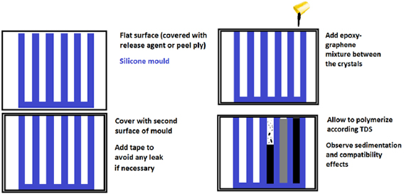
Figure VIII.3. Preparation of a vertical casting system for the evaluation of a graphene dispersion.
Download figure:
Standard image High-resolution imageIn the case of thermoplastics, a polymer adapted microtome which allows to obtain flat and smooth slices or ultrathin slices of the composite is needed [1311] and cryo-microtomography, working at temperatures between −15 to −185 °C, to avoid disturbing the positions or relocating NPs along the sample [1313, 1316]. The analysis of the graphene composites' mechanical and electrical properties is key to understand if the functionalization works properly, to improve the dispersion and interface.
By optical microscopy, even at low resolution, it is possible to characterize the effectiveness of functionalization, i.e. the homogeneity of the dispersion of GO in an epoxy composite, and the rate of decrease of large size aggregates.
VIII.3. Noncovalent functionalization of graphene
VIII.3.1. Functionalization in dispersion
Graphene can be exfoliated in water with the help of amphiphilic surfactants [182, 184]. Most published works use 'conventional' aliphatic surfactants (i.e. soaps) [182, 184]. However, stable dispersions can also be obtained using small polyaromatic dyes as surfactants [194, 214, 215]. Thanks to their aromatic core, these molecules can adsorb strongly on the graphene surface, forming also ordered layers [193], noncovalently functionalizing SLG/FLG. They have also a strong and unique absorption (molar absorption coefficient ε > 15 000 l g−1 m−1) and emission spectrum in the visible range, which allows to monitor their interaction with graphene in solution and in solid [216, 217]. Many of these molecules are also low cost dyes, already widely used in large-scale compounding of polymers, e.g. as industrial additives and colorants [218]. These molecules can exfoliate not only graphene but also a wide range of LMs, such as BN, WS2, MoS2, selenides and tellurides with concentrations up to 0.54 g l−1 [219].
Several pyrene derivatives with a varying number of polar functionalities were used as exfoliation agents [194]. A significant part of the solubilized material was composed of SLG (up to 22%), with most of the remaining material composed of FLG (50% to 60% <7L). The total concentration depends on the polar functionalization present on the pyrene core. Molecular dynamics calculations revealed that a critical factor is a one molecule thick solvent layer present between dye and SLG [194]. The amphiphilic molecule changes its orientation when approaching the surface to slide into this layer, and the asymmetric shape of the dyes facilitates this step. In these graphene organic hybrid systems, colloidal stabilization is achieved through electrostatic repulsion between charges introduced by the surfactant, and can be overcome by changing pH or adding salts [194].
VIII.3.2. Exfoliation in organic solvents
The use of small organic molecules acting as stabilizing agents is expected to promote LPE of graphite when molecules have a stronger affinity to graphite/graphene than the solvent/graphene interactions. A good starting point in terms of molecular design relies on the use of alkanes, which exhibit a high affinity (~2 kcal mol−1 per each methylene unit) for the basal plane of graphite/graphene [1315]. Ref. [230] reported that arachidic acid (C19CA) can promote the exfoliation of graphite in NMP. The addition of C19CA does not affect the quality and structure of the resulting graphene, as compared to NMP alone, highlighting the non-invasive nature of the process, but alkyl chain based stabilizers led to an increase of SLG (25%) and FLG (70% for 2–6 layers) [230].
The use of α-functionalized alkanes as stabilizers during LPE allows one to increase YW in liquid media. To understand the role of the functional group in α-substituted alkanes, Ref. [235] used the C21H43 alkyl chain as a scaffold and decorated it with simple, yet chemically distinctive groups: methyl, alcohol, amine, and carboxylic acid. The most effective exfoliation was obtained with docosanoic acid, with YW ~ 1.6%, with a ~100% increase when compared to control samples (0.8%). YW of LPE in docosane is ~1.35%, while docosanol and docosan-1-amine have lower performance (1% and 1.1%, respectively). The thermodynamic analysis in Ref. [235] suggests that aliphatic chains functionalized with carboxylic acid groups promote the stabilization of exfoliated SLG and FLG in NMP due to synergistic interactions between DSAs, surface, and polar solvent.
Ref. [231] also reported that the performance of linear alkanes exposing a carboxylic acid head group as stabilizers directly depends on the length of the linear alkane chain. 5 linear modules were explored: hexanoic acid (C6CA), lauric acid (C12CA), stearic acid (C18CA), lignoceric acid (C24CA) and melissic acid (C30CA), whose different adsorption energies on graphene and tendency to form tightly packed self-assembled monolayers on such a surface affect their performances as stabilizers. The analysis of carboxylic acid assisted LPE revealed that the concentration of graphene dispersions prepared in NMP, ODCB and TCB increases linearly with the length of the aliphatic chain. The dependence of YW with the length of the aliphatic chain was interpreted by means of a thermodynamic model of molecular self-assembly on graphene [231]. This showed that the shorter the aliphatic chain, the larger is the (rotational and translational) entropic cost of forming a 2d layered structure. These results suggest that a model based on molecular mechanics for the energetics and a statistical mechanic treatment of entropy, could be used to predict the efficiency of supramolecular building blocks as stabilizers and guide the chemical design of next generation stabilizers. Nevertheless, the role of kinetics cannot be fully ruled out.
Ref. [234] reported that alkoxy-substituted photochromic molecules can act as photo-addressable stabilizers to enhance YW in an upscalable molecule-assisted LPE-based method. The large conformational change associated with the trans–cis photochemical isomerization of alkyl-substituted azobenzenes can be used to improve YW. The simultaneous use of UV light, promoting the trans-to-cis isomerization, as well as thermal annealing at 40 °C and mechanical forces generated by sonication, both favoring cis-to-trans isomerization of 4-(decyloxy)azobenzenes, promotes the exfoliation of graphite in liquid media. The most effective exfoliation is obtained with azobenzene molecules irradiated with UV light in NMP at 40 °C, with a concentration of exfoliated graphene ~110 mg ml−1. This corresponds to an ~80% increase in YW when compared with pure NMP (63 mg ml−1). By depositing the hybrid film onto Au pre-patterned SiO2 substrates, light- responsive thin hybrid films, formed in a one-step co-deposition process, can be realized, whose conductivity can be reversibly modulated by the trans-to–cis photoisomerization of the azobenzenes. By combining this approach with cost-effective techniques, such as ink-jet printing, more complex responsive device designs and architectures may be realized.
VIII.3.3. Exfoliation with aromatic dyes in chloroform and THF, and further processing in polymers
Graphene can be exfoliated in water, using surfactants, or in high-boiling solvents such as DMF or NMP. For an effective, technologically competitive application of GRMs as additives in (nano)composites for electronics or structural applications it may be preferable to solubilize graphene in low-boiling volatile solvents, like CHCl3 or THF. However, the use of amphiphilic surfactants is not suitable to solubilize graphene in organic solvents whose polarity is low [193].
Ref. [193] used perylene diimide (PDI) molecules soluble in organic solvents as 'apolar surfactant' for exfoliation and successive processing in polymeric commercial films of poly(vinyl chloride) (PVC), to make them conductive. The PDI has an extended polyaromatic core (which can interact via π–π stacking with the GRM) and flexible side groups, with low, but tunable polarity that make these molecules soluble in a range of organic solvents (figure VIII.4).
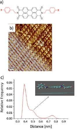
Figure VIII.4. (a) General formula of the PDI used for exfoliation. (b) STM image of the typical packing of PDI adsorbed on graphite. (c) Average distance of the side groups of the PDI from SLG, from molecular modeling. In the inset, a typical snapshot of the simulation. Adapted from [193], © 2016 WILEY-VCH Verlag GmbH & Co. KGaA.
Download figure:
Standard image High-resolution imageTransparent sheets of PVC (thickness 182 ± 4 µm) were dipped into chloroform dispersions of FLG and PDI at RT, a procedure already used for rubber [568]. They were then dried in air, to let the chloroform evaporate. The swelling process was completed in <3 min, and gave an increase of ~80% in volume. No further change of the swollen area/size was observed when the polymer films were left in the dispersions for >3 min. After the swelling treatment, the PVC samples showed a dark color due to the presence of the FLG as well as a bright fluorescence due to the PDI.
SEM images showed a dense coating of rectangular and polygonal shapes covering the surface. The sheets were not just deposited on the surface, but embedded into it, in some case reaching some microns (<10 µm). Control experiments by swelling in PDI only gave surface covered by PDI crystals, and no improvement of electrical conductivity. Typically, when deposited by conventional solution processing, GRM flakes tend to lay flat on a substrate [272, 277]. Due to the swelling, the flakes penetrate into the polymer in an isotropic way, in some cases protruding out of the surface [193]. An improvement of material hydrophobicity by ~40% was observed in all cases, with measurements of water contact angle increasing from 72° (blank PVC) to >100°. Rs decreased significantly, going from completely insulating to ~105 Ω sq−1, a value useful, e.g. for applications in antistatic coatings [1787].
VIII.3.4. Functionalization on substrate
VIII.3.4.1. Doping of CVD graphene via noncovalent interaction with thionylchloride
Halogenation, i.e. doping of graphene with halogens, is a process in which halogens, such as fluorine, chlorine, bromine and iodine, are either used to replace one of the carbon atoms or are attached to the graphene surface [1316–1320]. As for all doping or chemical modification, processes stability is of importance. Here the focus is on chlorination, as this has proven to be a reliable, stable way of halogenation, allowing SLG doping without losing transparency [1316].
In Ref. [1316] Rs ~ 30 Ω sq−1 using up to 5LG was achieved, while keeping a high transparency ⩾85%. Depending on whether the doping agent is an electron acceptor or donor, p- or n-type doping can be attained. To achieve a high doping level in the range 1013 cm−2, thionyl chloride (SOCl2) is recommended. SOCl2 induces p-type doping due to the higher electronegativity of Cl compared to C.
CVD-grown graphene is first transferred on glass. Thermal release tape was used for the transfer process [1316]. Different approaches for doping with thionyl chloride have been tested: last layer doping, where the last or top layer of 1 to 5LG was doped after all layers were transferred in a staggered fashion, or interlayer doping, where the top layer after each transfer of SLG/FLG is doped creating a doped surface in between the layers. The doping is achieved as follows [1316]: SOCl2 treatments are performed in a dry chamber by placing graphene/glass and 1 ml of liquid SOCl2 (avoiding direct contact) at 105 °C for 60 min. Doping of multilayer samples was performed by repeating the SOCl2 treatment after transferring and stacking each SLG/FLG.
Rs is then measured in a van der Pauw configuration (see section IX.3). Ref. [1316] suggested to use a large sample area ~4 × 4 mm2 to obtain a representative Rs. Figure VIII.5(a) plots Rs as function of N for interlayer doped and undoped samples. Rs = 1/neµ, where n is the doping level, e the elementary charge and µ the mobility. The mobility is affected by defects, therefore µ ~ 1/nD, where nD is the defect concentration. It is thus important to know doping and defect concentration. SOCl2 allows a nucleophilic substitution by Cl atoms, which selectively occurs on defective sites, without affecting the existing sp2 carbon bonds, therefore, without introducing any new defects [1316]. In order to verify this doping mechanism a controlled amount of defects was introduced in graphene by H plasma [1316].
Figure VIII.5. (a) Comparison of Rs of chlorinated and non-chlorinated CVD graphene as function ofN. (b) Transmittance for 1 to 5L G. Adapted from [1316].
Download figure:
Standard image High-resolution imageThe quality of graphene after doping can be assessed by Raman spectroscopy. It is important to follow the correct procedure to extract the correct doping level and defect density [1321, 1322]. Graphene with controlled amount of defects induced by mild H plasma showed a higher doping compared to a pristine, reference sample doped with SOCl2 under the same conditions, but without being subjected to H plasma. This shows that SOCl2 molecules selectively chlorinate defective sites in graphene. However, defects are always counter-productive for achieving low Rs and high µ. Thus, a compromise between doping and Rs has to be made. It is therefore more favorable to abstain from the introduction of defects by mild H plasma in order to achieve lower Rs, instead of inducing structural defects to which Cl will attach and increase the doping level.
The most critical point is the doping stability with time. Figure VIII.6 shows the Raman spectra of pristine, chlorinated and defective graphene (induced by H plasma) measured directly after chlorination and after 3 months. Pristine graphene shows a Pos(G) and FWHM(G) ~1583 cm−1 and 14 cm−1, while FWHM(2D) ~31 cm−1. I(D)/I(G) < 0.1. Therefore, the doping level is estimated ~100 meV. Hydrogenated graphene on the other hand shows D, D' and D + D' peaks as result of defect introduction via H plasma treatment with I(D)/I(G) ~ 1.65. The doping is estimated ~107 meV. This gives nD = 4 * 1011 cm−2. This confirms the presence of defects introduced by the plasma treatment with no change in doping. After chlorination of the plasma treated sample the doping is ~380 meV. This is higher compared to that achieved by doping pristine SLG, suggesting that SOCl2 molecules selectively chlorinate defective sites. The Raman spectrum of chlorinated graphene after plasma treatment shows a reduction I(D). This can be explained by the doping dependence of the D peak [1321]. This gives nD ~3 * 1011 cm−2 consistent with that of the hydrogenated sample before chlorination. Therefore, although the chlorination process is able to increase doping, the defect density remains unchanged, in agreement with the chemistry of the SOCl2 doping process.

Figure VIII.6. (a) 514.5nm Raman spectra of pristine, hydrogenated and chlorinated graphene after hydrogenation. (b) 514.5nm Raman spectra of chlorinated, Cl-SLG, and hydrogenated and chlorinated graphene (Cl-(H-SLG)) directly and after doping and after three months in ambient conditions.
Download figure:
Standard image High-resolution imageConsidering that after chlorination, one chlorine atom is attached to each defect and taking a charge transfer of 0.57 electrons [1317], i.e. each Cl takes 0.57 electrons from graphene to induce p-doping, the doping can be estimated from the defect concentration. As a result, the estimated defect density evaluated in hydrogenated graphene corresponds to a doping ~65 meV. This is the doping level introduced via additional defects by plasma etching. The doping of a chlorinated pristine graphene sample was ~304 meV. This is the doping introduced directly via chlorination. Adding these two contributions to the doping coming from only chlorination, the final doping level is ~370 meV, in agreement with the ~380 meV of the hydrogenated and chlorinated sample estimated from the Raman spectra measured directly after plasma treatment and doping with SOCl2.
To check stability, figure VIII.6(b) compares the spectra of chlorinated (Cl-SLG) and chlorinated hydrogenated graphene (Cl-(H-SLG)) recorded after three months. The initial doping levels are ~304 meV for doped pristine graphene and ~380 meV for doped hydrogenated graphene. After three months these are ~250 meV and ~350 meV. This shows that doping is stable over time.
UV–vis spectroscopy can be used to assess the optical properties of the chlorinated samples. Figure VIII.5(b) reports the transmittance of 1 to 5LG interlayer doped graphene using thionyl chloride. The transmittance is still ~85% even for the 5LG interlayer doped sample, making this attractive for applications where low Rs and high transparency are needed.
Solution based processes for halogenation of graphene were also proposed (see e.g. [1318, 1319]), Ref. [1320] used CVD grown FLG on Ni and transferred it on a glass substrate to induce doping by bromine vapor at RT in inert atmosphere: a glovebox with <0.1 ppm of O2 and H2O and nitrogen filled glovebag with 2000 ppm of O2 and 2500 ppm of H2O. Ref. [1320] reported Rs ~ 180 Ω sq−1 with a reduction in transmittance ~2%–3% with respect to pristine SLG. A drop of Rs from 1548 Ω sq−1 to 602 Ω sq−1 after exposure to Br for 60 min was reported [1320].
VIII.3.4.2. Functionalization with polycyclic aromatic hydrocarbons
Non-covalent functionalization of CVD graphene transferred to SiO2 was achieved via drop-casting of an aqueous solution of perylene bisimide 1 [1323]. The packing density of the perylene self-assembled monolayer (SAM) was related to the cleanliness of the SLG surface. Vacuum annealing prior to functionalization removes polymer and leads to a much higher denser perylene packing density than on untreated SLG [1323]. This is illustrated when the Raman spectrum and water contact angle measurements are considered (figure VIII.7). The increased relative intensity of the perylene Raman peaks (pale shading) when compared to the SLG peaks (dark shading) for the pre-annealed SLG versus the as-transferred one is indicative of a greater quantity of perylene on the surface. Likewise, high density packed perylene on graphene has the smallest water contact angle (58 °) compared to the as-transferred graphene sample (89 °) and low density perlylene sample (67 °). Again, this increased hydrophilicity indicates a greater number of molecules on the SLG surface for the pre-annealed film.
Figure VIII.7. (a) Raman spectra for high and low packing density perylene1 SAMs on as-transferred and pre-annealed SLG. Inset: Structure of perylene1. Water contact angles on (b) bare SLG, (c) low and (d) high packing density of perylene1 on SLG. Adapted from [1323] with permission of The Royal Society of Chemistry.
Download figure:
Standard image High-resolution imageSTM can be used to estimate the SLG cleanliness before and after annealing, figure VIII.8. An image of the resultant high packing density perylene SAM is in figure VIII.8(b). Analysis of the periodicity of the line profiles indicates that the perylene molecules pack together with the perylene cores perpendicular to the SLG surface, figure VIII.8. This is at odds with the common belief [1324–1326] that organic molecules with large conjugates systems will adsorb via π–π interactions between the conjugates core and SLG/FLG. This suggests that the method of deposition has a large bearing on the adsorption mechanism, as the liquid deposition process discussed here results in significantly more neighboring molecule-molecule interactions [1323] than another techniques, such as thermal evaporation.

Figure VIII.8. STM images of (a) as-transferred (top) and subsequently annealed (bottom) CVD-SLG on SiO2 and (b) after wet-chemical deposition of perylene1 on the same annealed substrate. (c) line profiles from (b) and (d) zoomed in area with molecular structure overlay. Adapted from [1323] with permission of The Royal Society of Chemistry.
Download figure:
Standard image High-resolution imageThis non-covalent functionalization was taken a step further by chemically modifying the functional end groups, as well as showing that perylene functionalization can successfully be carried out prior to polymer transfer to arbitrary substrates, creating a functional layer transfer (FLaT) [1327]. The latter finding is important, as it allows perylene SAMs of very high packing density to assemble on pristine SLG without having to anneal the as-transferred SLG to remove any polymer residues as depicted in figure VIII.9(a). Reacting ethylene-diamine (EDA) with the carboxylic acid groups of the perylene1 SAM using O-(7-azabenzotriazole-1-yl)-N,N,N,N'-tetramethyluronium hexafluorophosphate (HATU) was carried out to investigate the possibility of converting the carboxylic acid groups to amines [1327]. This would allow the use of perylene bisimide 1 as anchor in SLG-based biosensing.
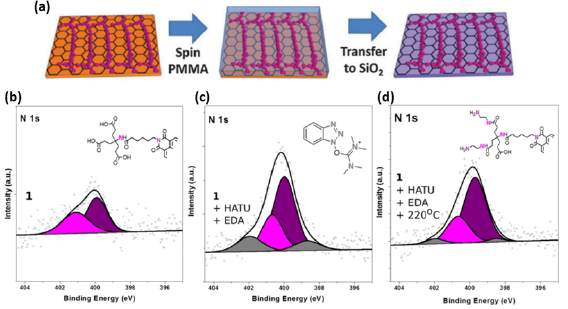
Figure VIII.9. (a) Schematic FLaT, in which perylene fucntionalised graphene is transferred b-d) XPS spectra of perylene on CVD-SLG for each derivitization step. (b) As-transferred perylene1 on SLG. Inset: Partial structure of perylene1 with corresponding nitrogen contributions. (c) Perylene1 on SLG after reaction with HATU and EDA. The two new contributions are from HATU residue. Inset: Chemical structure of HATU. (d) After annealing of derivatized sample at 220 °C. The HATU contributions reduce, but the amine signal increases. Inset: Partial structure of perylene1 after reaction, depicting corresponding nitrogen contributions. Adapted from [1327] with permission of The Royal Society of Chemistry.
Download figure:
Standard image High-resolution imageFigures VIII.9(b)–(d) show that after reacting perylene molecules with HATU and EDA new contributions can be seen in the N1s core level XPS spectra. The relative intensity of the peak component arising due to the presence of amine groups increases (pink), along with other contributions likely due to HATU residues (grey). Annealing the derivitized sample at 220 °C was found to reduce the relative intensity of these peaks, indicating that the any unreacted physisorbed surface contaminants are removed [1327]. These results show that it is possible to use perylene functionalized graphene as the basis for further chemical modification, towards biosensing applications.
The non-covalent functionalization, can then be, if needed, transformed also in covalent functionalization, triggering the covalent grafting of molecules self-assembled on graphene using, e.g., an electrochemical pulse (see section VIII.1 Electrochemical Functionalization) [1263].
VIII.3.4.3. Noncovalent functionalization with CNMs
Noncovalent functionalization can be used to fabricate heterostructures of graphene and CNMs [1328]. Figure VIII.10(a) shows a route to noncovalent chemical functionalization via assembly of all-carbon vertical heterostructures consisting of amino-terminated CNMs (NH2-CNM) on SLG produced by CVD on Cu foils [1328]. The chemically active amino groups of NH2-CNMs are located in these heterostructures in close vicinity to the SLG plane, as they are separated from it only by the ~1 nm dielectric CNM [81]. As shown by complementary spectroscopy, microscopy and electric transport measurements, the pristine SLG properties in these heterostructures remain unaffected [1328], which opens avenues for implementations in graphene-based electronic devices. In figure VIII.10(b), an optical microscope image of an NH2-CNM/graphene FET in the Hall bar geometry is presented. The structural quality of the device characterized by Raman mapping (figure VIII.10(c)) shows homogeneity. Figure VIII.10(d) presents RT electric-field effect measurements as a function of back-gate voltage, VBG, at 4 side contacts, figure VIII.10(b), P1–P4. The electrical characteristics are homogeneous on the scale ~3500 µm2. µ is nearly a factor of two higher (~3000 cm2 V−1 s−1) in the heterostructure devices in comparison to the starting SLG (~1500 cm2 V−1 s−1), figure VIII.10. This may results from a reduction of charge impurities at the SLG/SiO2 and SLG/ambient interfaces. Shubnikov–de Haas oscillations accompanied with resistivity plateaus of the quantum Hall effect at low T, figure VIII.10(f), demonstrate the high electronic quality in the engineered NH2-CNM/graphene heterostructures [107, 1328].
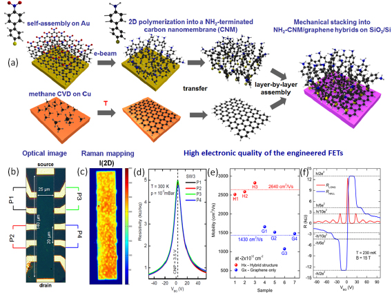
Figure VIII.10. Noncovalent chemical functionalization of SLG. (a) Schematic of the fabrication of NH2-CNM/SLG heterostructures via mechanical stacking of the individual sheets. (b) Microscope image of the fabricated FET with Au contacts in the Hall bar geometry. (c) Mapping of the Raman 2D peak on the active device area. (d) RT homogeneous electrical field effect at different side contacts of the FET as a function of VG. (e) µ of heterostructure and reference devices. (f) Quantum oscillations in a magnetic field at low T confirming high electronic quality of SLG in the heterostructures. Adapted from [1328] © Wiley-VCH Verlag GmbH & Co. KGaA.
Download figure:
Standard image High-resolution imageThe NH2-CNM/graphene FETs are promising for biosensors. As amino groups can further be functionalized with respective receptors, one could use NH2-CNM/SLG FETs as analyte-specific electrochemical sensors. GFET biosensors have a very high sensitivity up to the fM level [285]. However, this is difficult to achieve in combination with high selectivity and specificity of the biomolecular binding events. While any covalent SLG functionalization may affect the electronic quality, a functionalization via physisorption typically involves larger distances leading to the reduced sensitivity. Woszczyna et al [1329] used 1 nm dielectric and specifically functionalized CNMs to overcome these problems. It is also promising to use them in graphene-based electronics as a complementary dielectric, similar to hBN, for engineering top-gate electrodes, for field-effect tunneling transistors or in flexible electronic applications.
VIII.4. Defect functionalization of GRM
VIII.4.1. Edge modification of GRM in dispersion
Edge selective functionalization would be of particular interest to obtain engineered samples able to further react or assemble in a controlled way. Edge functionalization is in principle driven by the reactivity of the carbon atoms localized at the peripheral edges, which differs from the inertness of the C atoms on the basal plane due to the stability of the extended delocalized π-system. In fact, edges may be regarded as defects in the graphene structure, which can be exploited for its functionalization without severely disrupting the π-conjugated network [1329, 1330]. Edge functionalization may also be carried out on non graphene LMs in general [1246, 1331].
The diazonium chemistry of carbon nanostructures is one of the most convenient methods to covalently functionalize the edges of graphitic materials [1332–1335]. This reaction proceeds through a free-radical mechanism as a result of transfer of a delocalized electron from a graphitic substrate to the aryl diazonium cation to form an aryl radical after the release of nitrogen [1246] (figure VIII.11).
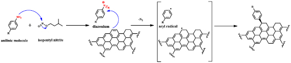
Figure VIII.11. Free-radical mechanism for edge-selective functionalization using diazonium species. Adapted from [1336], copyright American Chemical Society.
Download figure:
Standard image High-resolution imageThe standard protocol [1330], which generates the reactive diazonium species in situ from a stable anilinic compound in the presence of an alkyl nitrite (radical initiator), was followed by performing the reaction in DMF with different equivalents of the aniline derivative per carbon atom. In Ref. [1337], graphite flakes with lateral size ~10–50 µm and thickness ~10 nm, were first dispersed in DMF by bath sonication. Then, 4-aminophenol was added and the mixture sonicated. After that, isopentyl nitrite (6 equiv. per carbon atom) was slowly added to the dispersion and the reaction mixture was kept at 80 °C for two different reaction times, 24 and 48 h. After cooling to RT, the reaction was quenched by pouring the mixture into distilled water and filtration of the GRM dispersion through a PTFE membrane. The filtered cake was redispersed in DMF by ultrasonication and filtered through a PTFE membrane. This sequence was repeated twice with DMF, distilled water, methanol and diethyl ether, before obtaining the product after drying (figure VIII.12)[1337].
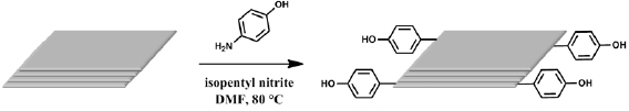
Figure VIII.12. Edge-selective functionalization with 4-aminophenol.
Download figure:
Standard image High-resolution imageFunctionalization of the flakes was confirmed by a dispersibility test in an organic solvent, where the functional groups present good solubility. Pristine and functionalized flakes were dispersed in IPA at a concentration of 0.1 mg ml−1 and sonicated for 30 min. After 2 days, chemically modified flakes with 2 and 4 equiv. of 4-aminophenol during 24 and 48 h, respectively, precipitated from the dispersion. The functionalized sample prepared with 4 equiv. of the anilinic compound using a reaction time of 24 h displayed better dispersibility and was the only sample that did not precipitate after a few days in IPA, which suggests the presence of a higher concentration of hydroxyl groups.
The chemical composition of pristine and chemically modified flakes was investigated by XPS. Upon functionalization, both the C–C sp2 content and the π-π* shake-up band decrease due to the disruption of the delocalized π conjugation in the graphitic structure, while the content of C–OH/C–N and >C=O/C = N increased. The O/C ratio increases from 1.7% to 8.2%, while the N concentration is ~3%–5%, ascribed to adsorbed molecules or residual solvents [1332, 1338].
The degree and selectivity of edge functionalization is influenced by N, edge states, degree of exposure of the interior basal planes and defects [1330, 1332]. In Ref. [1337], edge selective functionalization was maximized for 4-aminophenol and these conditions can be extended to para-substituted aniline derivatives. This opens new possibilities to modulate physical and electronic properties for diverse applications, such as catalysis and opto-electronics [1335, 1339]. Similar functionalization can be used to obtain building blocks for the design and manufacturing of functional materials.
VIII.4.2. Functionalization of SLG on substrate after introduction of defects
Ref. [1340] functionalized graphene on SiC with organic molecules forming covalent bonds. This is alternative to wet-chemistry protocols that reported covalent modification methodologies incompatible with some functional groups due to harsh conditions (such as high thermodynamic force, generally exceeding 20 kcal mol−1, or long reaction times, even more than 12 h) used e.g. diazonium salt, click chemistry or surface reactions [1227, 1232, 1244, 1253, 1341–1344].
Ref. [1340] reported the controlled atom-molecule substitution in ultra high vacuum (UHV, P < 2 × 10⁻¹⁰ mbar) by using p-aminophenol molecules, consisting of an aromatic ring with an amino and a hydroxyl group, linking the amino group to the graphene network and leaving free the hydroxyl group. This method was also successfully carried out on graphene grown on Ir.
The substrate was degassed by UHV annealing at 200 –400 °C (details depending on the type of sample) in order to remove physisorbed contaminations [1340]. This thermal treatment was performed by electron irradiation in a heating stage placed at the manipulator, while the annealing T was monitored with an IR pyrometer (emissivity ~0.9). After degassing, the cleanness of the sample was confirmed by STM [1340].
The next step consists in creating single atom vacancies (SAV) by bombarding SLG with low energy ions (Ar+). For this procedure, the sample needs to be placed close to the ion gun (10 cm maximum) at a 0°–15° incidence. The acceleration of the electrons inside the Specs IQE 11/35 ion gun should be 100–140 eV, 10 mA, having a controlled Ar pressure ~1 × 10⁻⁷ mbar. The most important parameter is the exposure time, that varies between 30 s−2 min for producing the desired density of mono-vacancies [1345–1348].
After irradiation, the sample is subjected to a thermal flash to remove the physisorbed Ar. This flash should not be longer than 5 min, reaching different T for each type of sample: 550 °C for SLG and 250 °C for QFSLG. It is important to check the mono-vacancies by STM as soon as possible. Defects are very reactive and they could get passivated with air contamination [1349, 1350].
After modifying the graphene network, the evaporation of organic molecules (P-aminophenol) followed. They need to be purified by turbo pumping for at least 6 h to remove impurities. Following this strategy, Ref. [1340] tested by STM that the organic molecules filled most of the SAV defects, as for figure VIII.13.

Figure VIII.13. STM images of the p-aminophenol molecules covalently anchored to the monovacancies created by the soft irradiation of the surface with argon ions in both types of samples: SLG (upper panel) and QFSLG (lower panel). The graphene on SiC was grown as for Ref. [611]. Note that in the images of the SLG sample one can see the (6 √ 3 × 6 √ 3)R30° reconstruction from the SiC buffer layer, whereas in the QFSLG sample only the graphene network is seen since intercalated hydrogen has decoupled the buffer layer. The molecules appear as protuberances inserted into the graphene network. Partially adapted from [1340].
Download figure:
Standard image High-resolution imageVIII.4.3. QFSLG
In order to check the covalent nature of the bonding of the organic molecules to the graphene lattice several experiments were conducted. Figure VIII.14(a) shows the XPS N 1s peaks corresponding to a p-aminophenol dosing of a sample with and without previous SAV defects. This points out the covalent nature of the bonding in the latter case. The thermal stability of the bond was tested up to T = 250 °C, figure VIII.14(b)). Even after annealing at this T, the XPS N 1s does not shift indicating the absence of breaking up of the A-AP molecule and that the covalent linked N remains in the graphene network.
Figure VIII.14. (a) N 1s core level spectra after dosing p-AP on a SLG surface without and with atomic vacancies. The N 1s binding energy corresponds to that of a C atom substitutional in the graphene-network. (b) thermal estability of the N 1s peak at RT and after annealing at ~250 °C.
Download figure:
Standard image High-resolution imageFunctionalization reaction mechanisms have been computed when the p-AP approaches the SAV either by the –OH or –NH2 terminating groups [1340] within the CI-NEB approach [916, 917] to get a converged minimum energy path. For approach by the –NH2 group, the molecular incorporation undergoes by a double (–NH2) dehydrogenation (see figure VIII.15). This process is efficiently catalysed by the SAV on the surface yielding energy barriers ~ 1.3 and 0.7 eV for the first and the subsequent second dehydrogenation, respectively, and a total enthalpy gain ~ 3 eV. The net enthalpy in the double (–NH2) dehydrogenation (~1.5 eV) is significantly higher than that corresponding to a single dehydrogenation of the OH group, pointing to a favoured incorporation of N atoms in graphene.
Figure VIII.15. (a) Schematic representation of the approaching of a generic NH2-terminated organic molecule towards a graphene SAV (with a magnetic moment of 1 µB). (b) For the case of p-AP molecule, most representative geometries for initial state, transition state and final state along the minimum energy path (MEP) for: (top) the first single dehydrogenation of the molecular –NH2 group, and (bottom) the second single dehydrogenation of the remaining molecular –NH group and the subsequent incorporation of the molecule via the N atom into the graphene lattice via the graphene SAV.
Download figure:
Standard image High-resolution imageVIII.5. Decoration with nanoparticles
The large surface area, electrical conductivity and mechanical strength make SLG a promising substrate to be coupled with NPsfor synergistic benefits in applications such as catalysis, energy storage, plasmonics and optoelectronics or solid state hydrogen storage [1351]. Depending on the Fermi level/work function of SLG and metal NPs, interfacial charge transfer can occur from SLG to NPs or vice versa. Hence, decorating with NPs is an efficient method for graphene doping with electrons or holes. To enhance interfacial charge transfer, a strong interaction between graphene and NPs is required [1351]. SLG can be decorated with NPs either by growing NPs directly on its surface, by mixing it with NPs, or by depositing NPs produced in the gas phase in UHV conditions.
VIII.5.1. Graphene-metal NPs
Graphene and other surfaces can be decorated with NPs via electroless plating [1352]. CNTs/SLG act as reducing agents towards metal salts. The Fermi level of nanocarbons allows them to spontaneously reduce Au3+ and Pt2+ salt solutions to form their respective M0(metal) NPs on the nanocarbon surface [1352]. To extend this to other metal NPs, reductive charging protocols can be used to increase the reducing strength of the nanocarbons. Fulleride, nanotubide and graphenide can be generated following reduction using alkali metal/liquid NH3 [1233, 1353, 1354] alkali metal naphthalide/THF [1355, 1356], or electrochemically in non-aqueous electrolytes [1357]. All reductive charging techniques insert electrons into the carbon π* orbitals, shifting EF, resulting in increased reactivity. Subsequent chemical reaction may take place via redox or electrophilic addition reactions that are believed to involve SET (i.e. radical based reactions) [1261, 1358–1362]. Due to the high reactivity of reduced nanocarbons towards oxygen and moisture in the atmosphere, these materials should be handled using inert gas filled glove boxes or Schlenk techniques [1363].
Ref. [376] used graphenides to reduce a series of Cu, Zn and Mg salts/complexes, to generate metal NPs on the SLG surface. KC8 and KC24 potassium-graphite intercalation compounds (K-GICs) were produced via the vapor transport [1363] from natural graphite, giving the corresponding characteristic bronze stage 1 KC8 and steel blue stage 2 KC24 compounds. For each experiment, anhydrous NMP was added to 10 mg K-GIC in a Young's tap Schlenk tube. The sample was removed from the glove box, mildly sonicated for 30 min and returned to the glove box for subsequent reactions.
MX2 (M = Mn, Zn and Cu) salts and Cu mesitylene (CuMes) were dissolved in NMP to yield 0.1 M stock solutions. Aliquots were added to the KCx dispersion to give the desired stoichiometry of metal to K. Typically, reactions are performed using the exact stoichiometry as the number of charges that are available for the reduction, e.g. for M2+ salts, M2+:K = 0.5:1, M+ salts, M+:K = 1:1, etc. It should be noted that the reduction potential of the metal salt/complex is shifted dependent on its concentration as defined by the Nernst equation [1364], ![${{E}_{{{{\rm M}}^{n+}}/{\rm M}}}/M=E_{{{{\rm M}}^{n+}}/{\rm M}}^{0}+\left( \left( {\rm RT}/n{\rm F} \right)\ln \left[ {{{\rm M}}^{n+}} \right] \right)$](https://content.cld.iop.org/journals/2053-1583/7/2/022001/revision1/tdmab1e0aieqn063.gif) , where E0 is the standard reduction potential, and n is the number of electrons involved. The reaction was left to stir for 72 h before being removed from the glove box, washed and filtered under vacuum with 100 ml each of NMP, water, chloroform and ethanol, and left to dry in air [376].
, where E0 is the standard reduction potential, and n is the number of electrons involved. The reaction was left to stir for 72 h before being removed from the glove box, washed and filtered under vacuum with 100 ml each of NMP, water, chloroform and ethanol, and left to dry in air [376].
Another approach for NP decoration is anchoring them to a polymer matrix surrounding SLG/FLG [1365]. EEG was prepared in Ref. [1365] with a sodium methanesulfonate aqueous solution as electrolyte. It was then dispersed in DMF and mixed with polyaniline (PANi, emeraldine base). The strong π–π interaction between PANi and EEG facilitated anchoring of PANi, achieving controlled surface functionalization. Subsequently, various colloidal NPs (Si, Fe3O4 and Pt) were added into the above PANi-functionalized EEG dispersion. During this process, NPs were bound to the amine/imine groups of PANi and assembled into EEG-PANi via electrostatic interaction and hydrogen bonding. Protonic acid doping of PANi with HCl generated EEG-NPs with sandwich-like nanostructures.
Plasmonic coupling of AuNP creates intense hot spots with large electromagnetic field-enhancements within the cavity formed by the two metallic surfaces [1721]. However, this localized field is extremely sensitive to morphological fluctuations and subtle changes in the dielectric properties of the cavity contents. SLG was used as an ultrathin spacer between AuNPs and a Au substrate to create plasmonic field enhancements [1721]. By gating, the possibility to produce plasmon tuning was demonstrated.
NPs can also be grown on SLG by gas phase synthesis [1366]. This approach was used to grow clusters (hence the name Ion Cluster Source or ICS [1367]). The ability to control the mean NP size (from 1 nm to few tens nm) with a quite narrow size distribution while keeping a high chemical composition has made ICS a versatile tool for the fabrication of NPs [1366]. The replacement of the single magnetron of the ICS by multiple magnetrons (Multiple Ion Cluster Source or MICS), offers the advantage of the synthesis of complex highly crystalline NPs with core–shell and core–shell–shell structures [1368–1370], hence providing multiple functionalities to the decorated material [1371, 1372].
One of the important issues in this fabrication method is the vacuum quality in terms of base pressure and purity of the injected gases. A good base pressure is needed (<5 · 10−9 mbar–5 · 10−7 Pa) in order to avoid contaminations. Ref. [1373] showed that small amounts of oxygen could modify the atomic structure of Au clusters. One can assume that other contaminants, such as C, N, He, etc could also affect the growth and properties of NPs. Therefore, it is crucial to obtain the best base pressure in the vacuum vessel. For the fabrication of the NPs in figure VIII.16, a base pressure below 5 · 10−10 in the MICS set-up was measured [1368–1370]. To ensure a minimum contamination, all gas pipes used to inject Ar and He are made of stainless steel and vacuum sealed. The purity of Ar and He was ~99.5% and >99.5% respectively. Additionally, the purity of Au was ~99.99% and a systematic pre-sputtering of the targets was performed for 4 min to remove possible contaminants adsorbed on the target surfaces. The samples were handled following basic precautions like using plastic tools, to avoid metallic contamination, [1374] flushing the fresh Si substrates with nitrogen, to remove dust, and depositing <4% of a monolayer of NPs to avoid NPs interactions [1375].

Figure VIII.16. Representative Cs-corrected STEM-HAADF images of (a) Ih, (c) Dh and (e) fcc NPs and (b–f) their corresponding size distributions for Ih, Dh and fcc, for Au NPs grown by MICS. The FFT and the model of each structure are shown as insets. The mean diameters are also given.
Download figure:
Standard image High-resolution imageThe structure and properties of NPs grown by gas phase synthesis is dependent on the parameters used in the cluster sources. Ref. [1376] reported that the power applied to the magnetron and the positioning of the magnetron inside the cluster source that defines the residence time of the NPs in the cluster source (and hence their size) can be used to tune the proportion of icosahedral (Ih), decahedral (Dh) and face-centered cubic (fcc) isomer structures. Therefore, a detailed description of the parameters is mandatory for any attempt to reproduce the growth of NPs by using the gas phase synthesis route.
The next step is the deposition of the NPs on SLG. a series of samples with different coverages are needed to evaluate the evolution of the SLG properties with increasing amounts of NPs. When using gas aggregation sources, the NP density is controlled by the deposition time. Once the number of NPs per time unit is known, one can calculate the time needed for a given coverage. However, if the calibrations are made on a different substrate, the different sticking coefficient will modify this value. The sticking coefficient of metallic NPs on SLG is 3 times SiOx as depicted in figure VIII.17).
Figure VIII.17. AFM of Au NPs (a) on SiOx and (b) on SLG after a deposition time of 4 s and 3 s, respectively, to illustrate the importance of the sticking coefficient.
Download figure:
Standard image High-resolution imageCharge transfer effects were explored between the AuNPs and graphene and compared with the doping achieved using other methods [1377], figure VIII.18. Depending on the functionalization method, different results are observed. When the decoration is driven through direct growth of NPs by chemical methods (red line, HAuCl4 [1377]) an increase of charge carrier concentration and a decrease in the surface potential as a function of the coverage is observed. This trend is not observed when the decoration is carried out with AuNPs deposited in UHV conditions (blue line). The effect of the latter method, where the AuNPS arrive already formed, is much subtler. This is the result of a smaller contact area between the UHV generated NPs campared to those synthesized by wet chemistry, since the cleaner UHV synthesis does not result in debris any debris in the NPs neibourhood.
Figure VIII.18. (a) Increment of carriers versus NPs density using UHV and wet chemistry Au salts methods, (b) surface potential versus density of Au, NPs using the UHV method or the wet chemistry Au salts method. After [1378].
Download figure:
Standard image High-resolution imageVIII.5.2. GRM as support to grow Mg NPs
For the synthesis MgH2NP a support is needed to better control the NP dimensions. GRMs are a possible alternative to other substrates such as porous carbon, CNTs or other carbon nanostructures [280, 1379–1386]. Ref. [1387] used graphite flakes as support and anhydrous tetrahydrofuran (>99%) and n-dibutyl-Mg. High purity hydrogen gas (99.999%) and graphite flakes with 12, 6 and 1.6 nm thicknesses and tens of microns in lateral size were used. Material processing was performed in a glove box filled with high purity argon (O2 and H2O < 1 ppm) to avoid oxygen contamination of the reactants preventing the formation of the Mg hydride.
MgH2 was synthesized by decomposition of n-dibutyl-Mg leading to the direct formation of MgH2 and under an inert atmosphere [1252] at 110 °C. A rapid formation of MgH2 is expected for higher T following the reaction [1388]:

In a typical synthesis protocol, n-dibutyl-Mg was mixed to THF or C6H12 in different proportions. The mixture was placed in a stainless steel reactor and porous carbon, MWNTs or FLGs added. THF is slightly polar (0.207), while C6H12 non-polar (0.0006). For this reason, different solubility in relation to the solvent used are expected. In addition, MgH2 is highly reactive toward organic molecules [1389]. Then the process of thermal degradation of n-dibutyl-Mg reagent is expected to be susceptible to the synthetic solvent utilized. Hence the use of different solvents in principle should lead to different MgH2 structures and hydrogen performances [1390].
Hydrogen was introduced in the reactor at a pressure of 10 or 20 bar and the solution heated at 170 °C and stirred at 50 rpm overnight [1391]. After 12 h, a black/gray precipitate was obtained from the decomposition of n-dibutyl-Mg. The suspension was then transferred in appropriate vessels under inert atmosphere and the main part of the solvent was removed by using a centrifuge at 5000 rpm (~2000 g). To further dry the material and remove the remaining organic residuals, the material was placed in a dynamic vacuum ~10−2 mbar for ~5 h. The exsiccated material was placed in sealed vials, to avoid Mg oxidation, for the characterization [1387, 1392].
Stabilization of MgH2NPs depends on the interaction between NPs and the support surface [1393–1395]. Defects and functional groups play an important role and a description of synthesis recipes should always be accompanied by a detailed description of the material. The TEM analysis showed crumpled surfaces (figure VIII.19). Curvature leads to higher reactivity of FLG towards chemical elements such as hydrogen or Mg [1394, 1396, 1397]. Wrinkles may then play an active role in limiting the formation of MgH2NPs in the solvent and enhancing the decoration of the graphene surface.
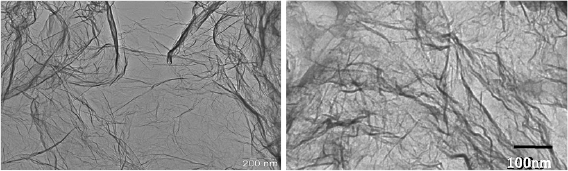
Figure VIII.19. TEM images showing wrinkles and crumpling.
Download figure:
Standard image High-resolution imageThe XPS analysis showed Mg in a completely oxidized form, because it difficult to introduce the sample in the XPS instrument avoiding exposure to atmosphere. The oxygen is ~34%. However, if oxygen is considered as exogenous due to atmosphere exposure, the quantification can be limited to C and Mg core lines. The Mg concentration corresponds to ~27%.
Lower reactant concentrations led to better results in terms of NP size. MgH2 NPs with size >5 nm were obtained after optimization. Nowadays the use of hydrogen for fuel cells is limited by the difficulties of synthesizing efficient storage materials. Mg offers a compromise between good hydrogen storage (7.6 wt%) and desorption T if compared to other materials. In addition, Mg is an interesting material because it is low cost and non-toxic. For Mg/MgH2 the enthalpy of reaction is ~75 kJ mol−1 H2, corresponding to a H desorption T ~350 °C [1398, 1399]. However the thermodynamic properties of this material can be improved lowering the Mg-H bond formation enthalpy. For practical application in automotive, the metal-hydrogen formation enthalpy should be ~30 kJ mol−1 H2 [1400, 1401]. It has been demonstrated both theoretically and experimentally that the reduction of the Mg particles affects the bond energy with hydrogen [280, 1402], although it is not easy to confine the Mg particle size to the nanometer scale. The possibility to synthesize Mg NPs on the nanometer size is then of great interest for both automotive and stationary applications. Materials on these size exhibit hydrogen desorption T~ 160, 140 °C [1387].
VIII.6. Functionalization of other LMs
VIII.6.1. Covalent functionalization of MoS2
VIII.6.1.1. Reductive covalent functionalization
Functionalization of MoS2 can be achieved by ligand conjugation of thiols at S vacancy sites either introduced by ion irradiation [1403] or naturally occurring after chemical exfoliation [1404, 1405]. Such methods are interesting but limited in their utility. Ref. [380] reported the first step toward a general route to functionalize TMDs by grafting functional groups to the exposed S atoms, with a sequence, based on intercalation, chemical-exfoliation and subsequent quenching of the negative charges on the MoS2 by organic halides or other strong electrophiles [379, 380]. In this functionalization sequence intercalated, chemically exfoliated MoS2 is reacted with electrophiles such as halides and diazonium salts (figure VIII.20). The use of chemically exfoliated MoS2 is beneficial due to the good exfoliation in water making LM both sides accessible. Chemically-exfoliated MoS2 can be obtained by reacting it with n-butyllithium (n-BuLi). This leads to the formation of a Li intercalation compound associated with a widening of the interlayer distance between the individual MoS2 layers and a charge transfer from n-BuLi to the MoS2. As a result of the charges residing on the MoS2 flakes, a destablilization of the semiconducting 2H-polytype is observed due to an effective change of electron density in the d orbitals of the transition metal [1406]. Chemical exfoliation after Li intercalation thus usually results in the formation of the 1T-polytype of MoS2 [1406]. It depends on the intercalation conditions to which extent this transformation occurs [379, 1407].
Figure VIII.20. Schematic of basal-plane functionalization of MoS2. After intercalation with n-butyllithium, the negatively charged MoS2 is dispersed in water by mild bath-type sonication leading to an efficient exfoliation into individual sheets. The charges on the MoS2 are quenched by the addition of 4-methoxyphenyldiazonium tetrafluoroborate obtaining the functionalized product. Adapted from [379], copyright American Chemical Society.
Download figure:
Standard image High-resolution imageIn contrast to negatively charged graphenides, the resultant material is reasonably stable under ambient conditions and can be dispersed in water [1406]. Due to this, the preparation of solvents used for the initial intercalation process is easier compared to graphene. Solvents only have to be dried and not necessarily freed from oxygen. For this purpose, it is recommended to distil and reflux the solvents (e.g. n-hexane and cyclohexane) two times over a Na wire under Ar atmosphere, prior to the use of the intercalation reagent.
Since MoS2 has long been considered to be unreactive and almost inert even after intercalation [159], Ref. [379] used very aggressive electrophiles: diazonium salts to quench the negative charges on the MoS2 and functionalize the material. After the final sonication step of the purified intercalate 4-methoxyphenyldiazonium tetrafluoroborate was dissolved in distilled water and added to the dilute yellowish/brownish MoS2 dispersion dropwisely under exposure to light. After addition of only a few drops of reagent, a black precipitate formed. The reaction mixture was stirred overnight and filtered. Material which passed through the membrane in the first step was collected and filtered again.
Washing with ~100 ml isopropanol to remove organic side-products, such as the correspondent biphenyl, and washing with distilled water yielded the functionalized MoS2 product after drying under vacuum (~ 10−2 mbar) at RT. The formation of a covalent C-S bond was evidenced by the appearance of a C-S stretching vibration in the IR spectra [379, 380], a new component in the S XPS core level spectra at higher binding energy [379, 380] and solid state NMR [380]. By XPS [379, 380] and thermogravmetric analysis coupled to mass spectrometry [379], it was possible to estimate the degree of functionalization. Typically, 10–20 atom% S bears a functionality [379, 380]. The degree of functionalization was shown to depend on the initial intercalation conditions: when a milder intercalation with a low n-BuLi to MoS2 stoichiometry ratio is used (three-fold molar excess of MoS2), the degree of functionalization is ~ 10 atom% [379], whereas it can reach up to ~ 20 atom% when n-BuLi is used in excess (three-fold molar excess of n-BuLi) [379, 380].
Here we provide a protocol for the fabrication of MoS2-templated conjugated microporous polymers (M-CMPs) by growing nitrogen-rich CMPs shells on both sides of 4-iodophenyl-functionalized MoS2 templates [1408]. The synthesis strategy for M-CMPs is illustrated in figure VIII.21. First, chemically-exfoliated MoS2 (CE-MoS2) was achieved by reacting bulk MoS2 with n-butyllithium (n-BuLi) [379, 380, 1408]. Then, it was functionalized with 4-iodophenyl diazonium salt under aqueous conditions [379, 380, 1408]. The obtained 4-iodophenyl-functionalized MoS2 (MoS2-I) can be well-dispersed in various organic solvents, such as toluene and DMF. Next, the arylacetylene building block 1,3,5-triethynylbenzene mixed with an aryl di- or trihalide was reacted with MoS2-I in anhydrous DMF in the presence of Pd(PPh3)4, CuI and Et3N under inert atmosphere. This Sonogashira-Hagihara cross-coupling reaction was carried out at 100 °C for 3 days under vigorous stirring and yielded an insoluble, crude product that was collected by filtration and purified by Soxhlet extraction with THF for 2 days. Sandwich-like M-CMPs with high specific surface areas and hierarchically porous structure were obtained after vacuum drying. As-prepared porous polymer-MoS2 sandwiches can be converted into the corresponding hierarchically porous MoS2/nitrogen-doped porous carbon hybrids by direct pyrolysis of the M-CMPs flakes. The hybrids are characterized by high specific surface areas and aspect ratios and showed a promising oxygen reduction reaction (ORR) and supercapacitor performance, due to the maximized interfacial interaction between nitrogen-doped porous carbon and MoS2 layers.
Figure VIII.21. Idealized formula scheme depicting the chemical exfoliation of bulk MoS2 and subsequent functionalization with 4-iodophenyl substituents under formation of MoS2-I, as well as the preparation of MoS2-templated conjugated microporous polymers (M-CMPs) and the corresponding MoS2/nitrogen-doped porous carbon (M-CMPs-T) hybrids. (i) monomers: 1,3,5-triethynylbenzene and 2,5-dibromopyridine, 2,5-dibromopyrazine, or 2,4,6-trichloro-1,3,5-triazine, argon, Pd(PPh3)4, CuI, Et3N, DMF, 100 °C, 3 d; (ii) argon, heating rate: 10 °C min−1, pyrolysis temperature: 700, 800, or 900 °C, 2 h.
Download figure:
Standard image High-resolution imageA pathway towards covalent functionalization of TMDs was established through the reaction between liquid-exfoliated MoS2 and various metal acetate salts [1409]. This involves functionalization of the semiconducting 2H-MoS2 polytype. Generating it requires treatment of the 2H material with n-butyllithium, necessitating safety steps when handling this harsh substance. Direct functionalization of 2H-TMDs removes the requirement to use this treatment. Acetate functionalization of LPE MoS2 was shown to stabilize the exfoliated flakes in IPA and acetone, rather than having to use toxic solvents such as NMP and CHP [1409]. Dispersions of exfoliated 2H-MoS2 in IPA were mixed with a given metal acetate dissolved in IPA. This mixture was then sonicated for 30 min and the functionalized 2H-MoS2 was separated and collected by centrifugation and washing [1409].
XPS analysis was performed on the thin films of material formed via vacuum filtration [1409]. The Mo 3d and S 2p spectral regions shown in figure VIII.22 demonstrate functionalization of the flakes after treatment with Cu(OAc)2. The Mo 3d core level displays a new doublet associated with MoS2, shifted to higher binding energies than the unfunctionalized 2H-MoS2 polytype, due to functionalization. The S2p core level exhibits a new spectral feature for the same reasons. Re-dispersing dried functionalized 2H-MoS2 flakes in NMP removed the functional groups [1409]. Figures VIII.22(c) and (f) show that the material returns to its original state without any permanent changes in the spectral features, indicating no permanent structural or chemical modification during functionalization with M(OAc)2.
Figure VIII.22. Fitted XPS Mo 3d and S 2p core level peaks for (a, d) 2H-MoS2 (a), (b, e) 2H-MoS2-Cu(OAc)2, and (c,f) defunctionalized 2H-MoS2-Cu(OAc)2. Adapted from [1409], © Wiley-VCH Verlag GmbH & Co. KGaA.
Download figure:
Standard image High-resolution imageThe most critical step is to provide sufficient energy when the liquid exfoliated MoS2 in IPA is mixed with the acetate salts. This was achieved by additional sonication using a tapered microtip with high local energy input [243]. When using a larger diameter tip (required to produce larger quantities), the degree of functionalization (i.e. the number of S atoms on the surface decorated by the functional group) drops to <20%. Furthermore, depending on the purity of starting MoS2 and water content in the IPA, the initial MoS2 dispersion is sometimes not colloidally stable and the MoS2 precipitates from the dispersion while leaving a deep blue colored supernatant. This is currently not understood, but likely related to MoOx impurities in the powder that form complexes with the IPA/H2O solvent. From our experience, a stable dispersion can be obtained by sonicating this precipitated MoS2 a second time. However, in such cases, the degree of functionalization was again lower than reported.
The number of functionalization procedures available is limited. These mainly use exfoliated metallic 1T-MoS2 and in some cases ligand conjugation to semiconducting 2H-MoS2. All these works [1229, 1404, 1788] do not focus and discuss on the location and how the functionalization takes place. To get this information a different approach has been developed for functionalizing exfoliated 2H-MoS2 with the organic electron donor of 1,2-dithiolane-based pyrene derivative [1412]. These works demonstrated the possibility of obtaining MoS2-pyrene nanohybrids, showing a preferential edge functionalization [1412]. This primarily occurs via sulphur addition along partially saturated zig-zag MoS2-S edges, preserving intact the basal structure of functionalized MoS2. A natural consequence of this finding is that chemical functionalization of exfoliated MoS2 should be similar to that of bulk material, where edge functionalization is likely to be predominant [1412, 1732]. Thus, this offers the possibility of direct transfer of functionalization strategies from bulk to exfoliated MoS2, e.g. transition metal doping of edge sites to improve catalytic behavior.
The interfacing of TMDs with photoactive species via robust covalent bonding needs to be exploited via the formation of hybrid materials. This is particularly true in the context of their ability to function as donor–acceptor systems upon photoillumination. This goal has been achieved via the realization of novel donor–acceptor hybrids based on the covalent functionalization of MoS2 and WS2 with 1,2-dithiolane-modified carbon nanodots (CNDs) [1413]. The excitation of CND-MoS2 and CND-WS2 at 370 nm showed ultrafast energy transfer from CNDs to both MoS2 and WS2, while at 425 nm, charge transfer in CND-MoS2 but not in CND-WS2 was detected [1413]. These excited state electron-transfer processes offer good opportunities for donor–acceptor-type hybrids for energy harvesting applications.
VIII.6.2. Noncovalent functionalization of MoS2
Perylene functionalization of CVD-grown MoS2 and WS2 was carried out in a similar manner as for SLG [1323, 1327]. MoS2 and WS2 grown on SiO2 were coated with aqueous perylene solutions creating a non-covalent functionalization. It was reported that the resulting perylene layer was suited to seed ALD growth of Al2O3 on 1L TMD flakes (figure VIII.23) [1414]. ALD directly on TMD flakes, while successful for N > 2, was unsuccessful on 1L. This was attributed to the electronic structure of 1L-TMDs, and their cleanliness [1414]. After functionalization with perylene1 the ALD growth of Al2O3 takes place uniformly across the sample. Thus the non-covalent functionalization provides a robust mechanism to seed thin films of dielectric materials on 1L-TMDs, a requirement for many device applications and for further functionalization.

Figure VIII.23. (a) Topography of MoS2 triangles after 27 cycles of ALD after seeding with a perylene bisimide derivative. The flakes are higher than the surrounding substrate. (b) Line profile along the line marked in (a). The step height is 1.9 nm. (c) Schematic representation of the structure of (a) as indicated by the scan. Adapted from [1414] with permission of The Royal Society of Chemistry.
Download figure:
Standard image High-resolution imageIX. Characterization methods
IX.1. Microscopies
IX.1.1. Optical microscopy
IX.1.1.1. Quantitative analysis of the optical microscopy images
Many optical characterization methods rely on the quantitative analysis of optical microscopy images [1, 1375, 1417–1419, 1421]. One can extract the contrast difference between GRM and substrate by analysing the red, green and blue channels of the digital images. For each camera channel the reflected intensity at the substrate and GRM can be measured and the contrast difference can be directly calculated.
Figure IX.1(a(l)) shows an example of a collection of epi-illumination (light reflected by the surface of the sample and then detected) mode optical microscopy images of MoS2 flakes with different N (previously determined by AFM) where the thickness dependent colour is evident. The contrast difference requires an initial calibration, using an alternative thickness determination method, and it might slightly change from one experimental setup to another one as it relies on the spectral response of the employed digital camera, the microscope lamp emission spectrum, and the numerical aperture of the microscope objective.

Figure IX.1. (a)–(l) Color optical images in epi-illumination mode of MoS2 flakes with N = 1–12 a 300 nm SiO2/+ Si. The scale bar is 5 µm. (m) Thickness dependent contrast difference extracted from the red, green and blue channels. Figure reproduced from [1416], © Tsinghua University Press and Springer.
Download figure:
Standard image High-resolution imageIX.1.1.2. Multispectral imaging
Multi-spectral imaging characterization of GRMs was introduced by Refs. [1418, 1419, 1420] to identify N for graphene flakes on SiO2/Si substrates and it has been rapidly adapted to characterize and identify other GRMs [1416, 1421–1425]. The method involves the acquisition of optical images using narrow bandpass filters to select the illumination wavelength. The optical contrast, CT, is typically extracted from these images in order to obtain a quantity that does not depend on the illumination intensity. CT is typically defined as:
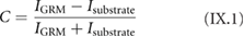
where IGRM and  are the reflected intensities from GRM and substrate. A quantitative analysis can be done on the basis of a Fresnel law based model, where the system is modelled as a stack of different optical media under monochromatic illumination in a normal incidence configuration [1418, 1419, 1426]. Hereafter the subscripts 0, 1, 2 and 3 will be used to refer to air, GRM, SiO2 and Si. First we focus on the case where only air, SiO2 and Si are considered. The Si layer is modelled as a semi-infinite slab whose optical properties are determined by its complex refractive index ñ3(λ) that strongly depends on the wavelength (λ) [1431, 1432, 1426]. The SiO2 layer, with a thickness d2, is modelled with its refractive index n2(λ) that also depends on the wavelength [1418, 1419, 1426].
The total amplitude of the light beam reflected by the SiO2/Si substrate (r) can be obtained from the infinite sum of light beams coming from the multiple reflections in the central SiO2 layer (see figure IX.2). Anytime that a light beam reaches an interface the Fresnel equations are applied, considering both the real and the imaginary part of the refractive index and accounting for the phase shift between the different light beams. E.g. the phase shift between the reflected beams at the air/SiO2 and those transmitted through the air/SiO2 (going across the SiO2 then getting reflected at the SiO2/Si interface then going across the SiO2 and finally being transmitted at the SiO2/air interface) is 2Φ2 (see the sketch in figure IX.2) with Φ2 = 2πn2d2 · cos(θ2)/λ. All this being considered, the total amplitude of the reflected light by the SiO2/Si substrate (r) is:
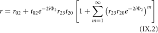
where rij and tij are the amplitude of the beam reflected and transmitted at the interface between the media i and j . These coefficients rij and tij can be obtained directly from the Fresnel law. Considering that rij = −rji and tijtji − rijrji = 1 and summing the geometrical series
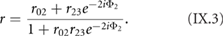
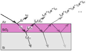
Figure IX.2. Sketch of the optical beam path transmitted and reflected at the different interfaces in a multilayer structure air/SiO2/Si to understand the role of the different optical paths on the optical contrast. Adapted with permission from [1427].
Download figure:
Standard image High-resolution imageThen the intensity of the light reflected by the SiO2/Si is Isubstrate = |r|2.
Under normal incidence assumption this expression is simplified because rij = (ñi − ñj )/(ñi + ñj ) and Φ2 = 2πn2d2/λ. When a GRM is placed on the SiO2/Si substrate, the intensity of the light reflected by the stack can be calculated in a similar way as Isubstrate:

Although the previous approach is general and it can be applied to stacks with an arbitrary number of media, it might become cumbersome to calculate the intensity of the light reflected by stacks with more than 3 media. The transfer matrix formalism is the most appropriate approach to analyse the light propagation in systems formed by a stack of many different media. From the previous expressions one can deduce that if one determines the GRM thickness (e.g. with AFM) it is possible to use the optical contrast measured at different illumination wavelengths to determine the GRM refractive ñ = n − iκ [1419, 1421, 1424, 1428–1430]. On the other hand, if the GRM refractive index is known one could determine its thickness directly from the measurement of the optical contrast acquired at different wavelengths with no need of AFM (figure IX.3).

Figure IX.3. (a) Optical images of a TaSe2 flakes with regions with different thicknesses, acquired at different wavelengths. (b) Optical contrast as a function of thickness for different wavelengths. The experimental data (circles) can be reproduced by the Fresnel law based model by using the refractive index for bulk TaSe2 (solid lines). Reproduced from [1416], © Tsinghua University Press and Springer.
Download figure:
Standard image High-resolution imageIX.1.1.3. Hyper-spectral imaging
In this technique the illumination wavelength is selected with a tuneable light source, e.g. based on a halogen lamp and a monochromator, instead of using narrow band pass filters [1431]. Figure IX.4 shows a schematic setup for transmission mode hyperspectral imaging. Epi-illumination hyperspectral imaging (or reflection mode hyperspectral imaging) can be also done with minimum modifications of the setup [1432].
Figure IX.4. (a) Schematic setup for transmission mode hyperspectral imaging. (b) Data acquisition process: optical images are acquired while the wavelength is varied. The resulting dataset is arranged in a 3d matrix. (c) Spectral information extracted from the dataset. The inset shows a transmittance spectrum obtained by normalizing the GRM spectrum to that of the substrate. Adapted from [1431], © IOP Publishing Ltd.
Download figure:
Standard image High-resolution imageHyperspectral imaging is carried out by sweeping the excitation wavelength in steps and acquiring a microscope image of the sample for each wavelength. The acquired images are then arranged forming a 3d matrix, being the first two matrix indexes the X and Y spatial coordinates and the third index (λ) the wavelength (figure IX.4(b)). Spectral information of a certain sample region can be directly obtained by plotting all the elements of the matrix along the wavelength dimension λ for fixed X and Y coordinates (figure IX.4(b)). Figure IX.4(c) shows a sketch of two spectra extracted from two regions in the sample: substrate (red) and GRM (blue). The GRM transmittance (Tr) can be obtained by dividing both spectra: Tr = IGRM/Isubs (inset in figure IX.4(c)), where IGRM is the intensity acquired on the GRM and Isubs that of the substrate. The absorbance A can be obtained from as: A = −log10 (Tr).
Figure IX.8 shows an example of characterization of GRM by means of hyperspectral imaging. The panels (a) to (f) show transmission mode optical images of a MoS2 flake for different wavelengths. From the collection of hundreds of images from 400 to 1000 nm one can extract the absorbance, figure IX.5(g).
Figure IX.5. (a)–(f) Transmission mode images of a MoS2 flake acquired at different wavelengths, selected with a tuneable monochromatic light source. (g) Absorbance versus wavelength, extracted from the sequence of MoS2 images on a flake with regions of different thicknesses (N = 1–6), for different wavelengths. Adapted from [1431], © IOP Publishing Ltd.
Download figure:
Standard image High-resolution imageIX.1.1.4. Micro reflectance/transmittance spectroscopy
In this method one illuminates the sample with white light and the reflected/transmitted light is analysed with a spectrometer (see figure IX.6) [1198, 1310, 1428, 1429, 1433, 1434]. The acquired reflection/transmission spectra can be analysed with the Fresnel law to extract information on the GRM optical properties. In figure IX.7 the refractive index of 1L-MoS2 is determined by fitting the measured optical contrast on different SiO2/Si substrates to the Fresnel law based model, using the refractive index of 1L-MoS2 as a fitting parameter (panel a) [1428]. The resulting values of the real and imaginary part of the refractive index are displayed in figure IX.7(b) and compared with bulk MoS2.
Figure IX.6. (a) Setup to characterize GRMs with micro-reflectance. (b) CVD grown MoS2 studied by micro-reflectance. Two spectra are acquired on (A) MoS2 and on (B) the SiO2/Si substrate and the optical contrast is extracted from them. Adapted from [1428], CC BY 4.0.
Download figure:
Standard image High-resolution image
Figure IX.7. (a) Optical contrast for 1L-MoS2 on SiO2/Si with different SiO2 thicknesses. The datapoints are fitted to a Fresnel law using the refractive index of 1L-MoS2 as fitting parameter. (b) refractive index of 1L-MoS2, compared with the bulk value. Adapted from [1428].
Download figure:
Standard image High-resolution imageOne can also obtain the dielectric functions from the measured reflectance spectra by means of a Kramers-Kronig constrained analysis of the spectra of GRMs on transparent substrates [1198]. From the resulting dielectric function, the refractive index can be calculated [1198]. Figure IX.8 shows an example of determination of the dielectric function from the reflectance spectra of 1-4L TMDs. From the resulting dielectric function, the absorption spectra refractive index can be calculated [1198].
Figure IX.8. (a)–(d) Reflectance spectra for 1L-MoSe2, WSe2, MoS2, WS2. (e)–(h) Real part and (i)–(l) imaginary part of the dielectric function. Adapted from [1198], © Springer Nature.
Download figure:
Standard image High-resolution imageAnother feature of micro-reflectance/transmittance measurements is their speed, each spectrum can be acquired in ~1 s, allowing one to characterize large scale samples (e.g. films grown by CVD, cm2 area) at hundreds of different locations to get an insight about uniformity [1429]. Figure IX.9 shows a differential reflectance spectrum acquired at one position on a 1L-MoS2 grown on sapphire. It also plots the histograms of the energy and FWHM of the A and B excitons measured at 550 different locations to characterize the sample homogeneity.

Figure IX.9. (a) Differential reflectance of 1L-MoS2 grown on Sa. (b) and (c) Histograms of A and B exciton energy for 550 flakes. (d) and (e) Histograms of FWHM of A and B excitons. Adapted from [1429], CC BY 4.0.
Download figure:
Standard image High-resolution imageIX.1.1.5. Comparison between multispectral, hyperspectral and micro-transmittance
Figure IX.10 compares different optical microscopy characterization methods, studying the same system: multi-spectral, hyper-spectral and micro transmittance of 1-3L-MoS2 [1421, 1431, 1434]. Table IX.1 compares the area characterized, the spectral resolution, and the time to carry out one measurement. This shows that micro transmittance/reflectance is a powerful tool to perform fast measurements in one spot, due to its high spectral resolution and low measurement time. The short measurement time allows one to perform point measurements at hundreds of different locations[1429]. Multi-spectral and hyperspectral imaging are very interesting to study large areas as in one shot ~10 000 µm2 can be measured at once, allowing for the acquisition of spatially resolved maps with diffraction limited spatial resolution [1435].

Figure IX.10. Comparison between different methods to measure the optical properties of 1L, 2L,3L-MoS2. In multispectral imaging narrow bandwidth filters (10 nm FWHM) are used to select the wavelength (the wavelength resolution is limited by the number of filters). In hyperspectral imaging, the illumination is provided through a white light source connected to a monochromator (2–3 nm resolution). In micro-transmittance, white light is collected through an optical fiber (acting as a confocal pinhole) and sent to a CCD spectrometer (~1 nm resolution). Adapted from [1436].
Download figure:
Standard image High-resolution imageTable IX.1. Comparison between different optical microscopy methods.
| Method | Area | Spectral resolution | Measurement time |
|---|---|---|---|
| Multi-spectral | ~10 000 µm2 | ~20–100 nm | 10–30 min |
| Hyper-spectral | ~10 000 µm2 | ~1–5 nm | 30–60 min |
| Micro transmittance | ~1–4 µm2 | ~1 nm | ~0.1–5 s |
IX.1.2. AFM
IX.1.2.1. LPE GRMs
AFM provides fast (<10 min/measurement) and reliable characterization of the lateral size and thickness distribution of flakes deposited on different substrates, allowing one to investigate large areas (hundreds of µm2) and to collect data from hundreds of flakes (figure IX.11(c)). The size distribution can be roughly modelled using a log-normal distribution, as observed for a range of GRMs exfoliated in the liquid including graphene [178], hBN [1437], MoS2 [185], WS2 [186], GaS [188] and black phosphorus [190]. More extensive statistical studies, performed on GO flakes using AFM, SEM and fluorescent microscopy, demonstrated that the fragmentation process can be described by a series of rupture-like breakup events, yielding two different populations of flakes featuring different size distributions [136].

Figure IX.11. (a) SEM micrograph of bulk BN flakes. (b) Solutions of exfoliated BN in isopropanol. (c) AFM image of BN flakes on SiO2. (d) Individual BN flake. (e) Histogram distribution of flake sizes. From [1437], with permission of The Royal Society of Chemistry.
Download figure:
Standard image High-resolution imageWhen working with LPE samples for AFM analysis, it is critical to avoid re-aggregation during solvent evaporation. For this, drop-casting the dispersion on pre-heated wafers (10 µl per 0.5 × 0.5 cm2 wafer) is often used [245]. The solvent evaporates and bubbles are formed, resulting in more uniform deposition compared to drop casting at lower T. The wafer should be heated to ~50 °C–70 °C above the boiling point of the solvent.
In the case of surfactant-based dispersions, it is recommended to dilute the sample with water (rather than surfactant) prior to deposition and wash the wafer thoroughly with water and isopropanol (~5 ml each) to remove residual surfactant. Residual surfactant can make thickness measurements very tedious, especially for very small flakes that are more difficult to distinguish from the surfactant. In this case, phase images can provide a guide as they usually give a good contrast between different materials. If problems with residual surfactant persist, the substrates can be soaked in water overnight without significant loss of flakes. Deposition from high boiling point solvents, such as NMP, may be challenging, and re-aggregation, residual solvent, or polymerized NMP covering flakes are observed. In order to overcome this problem, it is advisable to transfer the material exfoliated in NMP to IPA by centrifugation prior to AFM [190].
Si substrates with a 200–300 nm SiO2 enable flakes to be seen with an optical microscope/optical [1419]. This is a useful guide to identify regions of interest for imaging. Measured, apparent AFM heights of LPE GRMs are overestimated due to the presence of residual solvent. In general, accurate height measurements on inhomogeneous surfaces (such as flakes deposited on a substrate) are challenging due to contributions from capillary forces and adhesion, which depend on the material and measurement parameters [1438, 1439]. In addition, crosstalk between electrostatic and topographic signals [1214, 1215] can occur, leading to a bias of the height. To overcome these problems and obtain N from apparent height values, a step height analysis procedure was developed in Refs. [176, 185, 186, 190]. Incompletely exfoliated flakes showing clear terraces are first examined and the height of a various steps are recorded. These terrace step heights will always be a multiple of the apparent 1L thickness. The apparent measured SLG height can be 1–2 nm, much greater than the theoretical thickness [176, 185, 188, 190, 240, 1407]. Raman and PL analysis can be conducted in order to make sure that the thinnest objects measured are really SLG [176, 185]. The apparent SLG height can then be used to convert the apparent measured AFM thickness to N. For statistical analysis, it is recommended to record the height of at least 100–150 flakes. If the thickness varies across the flake, the mean value should be taken. From such statistical analysis, population histograms can be constructed. These are typically log-normal [185, 186, 188, 190, 1437] (also in the case of flake length). If this is not the case, the counting and/or imaging may be biased. e.g., if reaggregated rather than individually deposited flakes are included in the counting, this will lead to a deviation from the log-normal shape at the thicker end of the thickness distribution histogram. On the contrary, if surfactant and solvent residues are included in the counting, a deviation is obtained on the smaller end of the length distribution histograms. From these histograms and the statistical analysis, the arithmetic number mean for length and thickness is obtained.
Since AFM can be used to measure both flake thickness and lateral dimensions, for each flake of a given thickness, the volume can be estimated as thickness (N) × length(L) × width(w). This allows for the calculation of the volume-fraction-weighted mean layer number,  , where the summations are over all flakes. This is an alternative measure of thickness which reflects the fact that mass the tends to be concentrated in thicker flakes (the difference between arithmetic and volume fraction weighted mean is akin to the difference between number-average-molecular-weight and weight-average-molecular-weight in polymer physics [1440]). Arithmetic and volume fraction weighted mean values are typically related linearly, therefore both are an adequate measure of thickness [236].
Conductive SPM, like Kelvin probe microscopy (KPM), beside imaging capabilities, can be used to investigate charge transfer in exfoliated GRMs [277], while conductive AFM, providing localized current injections, can be used to locally modify the GRM chemistry, e.g. directly drawing conducive paths in GO films on SiO2 [1441].This can also be used to probe other electronic properties, such as piezoelectric effects [1442].
IX.1.2.2. Grown and transferred GRMs
When referring to grown materials measured heights can be affected by artefacts, i.e. crosstalk between electrostatic and topographic signals [1443, 1444], or can be overestimated due to the presence of adsorbates between substrate and 1L-GRMs [1445]. By combining two of the most employed measuring modes (contact and dynamic), these can be minimized and more accurate height values obtained. Recording secondary signal channels such as phase (in dynamic mode) or lateral force (in contact mode) is useful in revealing information such as different local mechanical and/or electrical properties [1446] or different polymorphic structures [1447] sometimes difficult to detect, or even hidden, in topographic images [1443–1445, 1447]. Dynamic and contact modes measurements can be performed at RT, purging the chamber with N2 to decrease the relative humidity and minimize capillary forces between tip and sample surface. Details about measuring modes in AFM can be found in Refs. [1448, 1449].
Figure IX.12 shows representative images of graphene layers grown on different substrates acquired in dynamic mode. In this mode, which employs the oscillation amplitude as feedback parameter [1448], the durability of the AFM probes (i.e. tip sharpness) is usually larger than in contact mode, since the tip gently [1450] taps the surface during the scanning [1446, 1451]. Probes with nominal force constant values ~3 nN nm−1 and resonance frequencies ~75 kHz are used. The most characteristic features are the pleats, commonly referred to as wrinkles, figure IX.12. These correspond to pleated/folded SLG due to released stress caused by the differences in the thermal expansion coefficients between SLG and the substrate, during cooling after growth [1452, 1453], or to local accumulation of carbon material at defects between coalescing grains of different orientation [630]. The maximum scanned areas are limited by the morphology of the substrate. For Cu foils this is usually <5 × 5 µm2, due to the high overall roughness that can exceed several hundreds of nm for those areas. For graphene on SiC, the scanned area is only limited by the piezo range thanks to the flatness of the SiC wafer [627, 630] (for chemical mechanical polished on-axis wafers).
Figure IX.12. AFM topographic images measured in dynamic mode of SLG grown on (a) Cu foil by PDV, (b) SiC(0 0 0 1 by CVD, (c) quartz by r-(ECR-CVD) [774] z-scale: 0–12 nm.
Download figure:
Standard image High-resolution imageIn dynamic mode, phase images can be acquired simultaneously with topography. Phase contrast is generally ascribed to differences in local energy dissipation and can reveal local mechanical and/or electrical properties [1446, 1451]. As shown in figure IX.13, this signal can be very useful to identify areas of different thickness. Top and bottom images in figure IX.13(a) illustrate this case, where circular brighter patches corresponding to BLG areas and are distinguished in phase imaging due to their different dissipative properties arising from mechanical and electrostatic difference as a function of N [1454]. Damaged areas in transferred layers (figure IX.13(b)) or covered areas in sub-SLG growth (figure IX.13(c)) can be identified in phase images. However, phase images can also be misleading since the contrast is very sensitive to the measuring parameters (oscillation amplitude and control setpoint [1455, 1456]). This is shown in figure IX.14, where phase contrast can be turned on and off at will, and even reversed, by changing the measured amplitude. There is no fixed recipe that ensures a good phase contrast, and tuning of the measuring parameters is necessary. Small amplitudes and amplitude set-points > 50% of the cantilever free amplitude usually enhance the phase contrast [1456]. The main disadvantage of using dynamic mode stems from the possible crosstalk between tip and sample surface. This is particularly critical in heterogeneous surfaces, with areas presenting different mechanical, electrostatic and/or hydrophobic/hydrophilic nature, and can lead to wrong N determination [1443, 1457]. This is illustrated in figure IX.15 graphene on quartz at submonolayer coverage. The thickness of the flakes measured in dynamic mode is ~3 nm, almost twice that in contact mode. This is due to the influence of uncompensated electrostatic forces, particularly affecting samples grown on insulating substrates. Ref. [1443] suggested to use KPM to avoid this problem [1452]. However, when dealing with insulating substrates, like in figure IX.15, it is not so straightforward, and the alternative is switching to contact mode (figure IX.15(b)). In contact mode, the lifetime of the probes is usually shortened compared to dynamic mode [1448] (tip radius increases after successive scans and resolution worsens), but height artefacts as those shown in figure IX.15 are seldom encountered. Commercial probes of low force constant (0.05–1 nN nm−1) are used to minimize damage to the sample. Similar to the dynamic mode, secondary signals can be recorded when measuring in contact [1458]. Lateral force imaging can reveal differences in friction between tip and surface [1458]. This is particularly interesting GRMs since they usually present a low (<0.1) friction coefficient [1459], which yields images like figure IX.16.
Figure IX.13. Simultaneous topographic (top row) and phase (bottom row) AFM images in dynamic mode of (a) and (b) CVD-graphene transferred to SiO2. (c) Flakes grown by r-(ECR-CVD) on quartz at submonolayer coverage.
Download figure:
Standard image High-resolution image
Figure IX.14. Simultaneous topographic (top row) and phase (bottom row) AFM images measured in dynamic mode of graphene flakes grown by r-(ECR-CVD) on quartz at submonolayer coverage. (a) Phase contrast between graphene and substrate disappears in the center of the image after changing the amplitude setpoint. (b) Phase contrast between graphene and substrate is reversed at the bottom of the image by increasing the amplitude setpoint.
Download figure:
Standard image High-resolution image
Figure IX.15. Topographic images of graphene flakes on quartz measured in (a) dynamic and (b) contact mode. Bottom: height profiles from the corresponding lines marked in the above images. The thickness measured on the same sample is different, depending on the mode used.
Download figure:
Standard image High-resolution image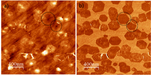
Figure IX.16. Simultaneous (a) topographic and (b) lateral force images of graphene flakes on quartz measured in contact mode. Dotted circles mark flakes location, hardly distinguishable in topography, but resolved in lateral force images.
Download figure:
Standard image High-resolution imageThe SLG areas are distinguished in lateral force images, facilitating flakes location, coverage quantification and size analysis. With lateral force images it is also possible to visualize the internal structure of SLG grains, masked in topographic images due to surface roughness. In figure IX.16, lateral force images reveal the multilayer structure of some flakes.
To better visualize these internal features in graphene flakes, soft tips (0.05 nN nm−1) and forces between 5 and 10 nN are recommended to avoid wear [1455]. Lattice-resolved lateral force images can also reveal the lattice periodicity, figure IX.17. To acquire these images, small scans are performed (5–20 nm lateral sizes), at frequencies ~2–3 Hz, with low feedback parameters. Applied forces are ~5–15 nN. These images do not correspond to true atomic resolution like routinely measured in STM, but lattice orientation and average lattice parameters can be determined.

Figure IX.17. Simultaneous (a) topographic and (b) lateral force images of graphene flakes on quartz in contact mode. The multilayer structure of some flakes can be distinguished in lateral force images. (c) High resolution lateral force image. Right: high resolution image acquired at the marked area. Inset: fast Fourier transform (FFT) of the high-resolution image to better observe the lattice periodicity.
Download figure:
Standard image High-resolution imageThe AFM tip can also be used to displace the samples. Ref. [774] swept the tip to determine N in fully covered samples. This should be used as last resort, after morphological characterization, since the tip can be irreversibly damaged due to the high (>100 nN) forces needed to remove the material. This damage can be visualized by recording force-distance curves prior and after sweeping. Figure IX.18(a) compares these two curves, and shows that adhesion is one order of magnitude larger after the experiment. This is mainly due to the increase in tip radius, which translates in a worsening of the resolution [1460, 1461]. Taking this into account, sweeping experiments should performed as follows. 1) an area is scanned either in dynamic or contact mode to check the morphology prior to sweeping. 2) contact mode is selected, and the same area (2–5 µm lateral size) is repeatedly scanned while increasing the scan rate (5–10 Hz), decreasing the number of points (256/128) and increasing gradually the applied force. By controlling the topography and lateral force signals, one can detect the onset of the removal of the material. Once the critical applied force is reached, the scanning is repeated during several images to ensure the complete displacement of the material. 3) To visualize the swept area it is recommended to switch to dynamic mode, to avoid spreading the accumulated material at the edges of the scanned area. To acquire final image is better if the scan is performed at 90°, since debris are accumulated at the lateral edges (fast scan direction). Figure IX.18(b) summarizes the results of this procedure.
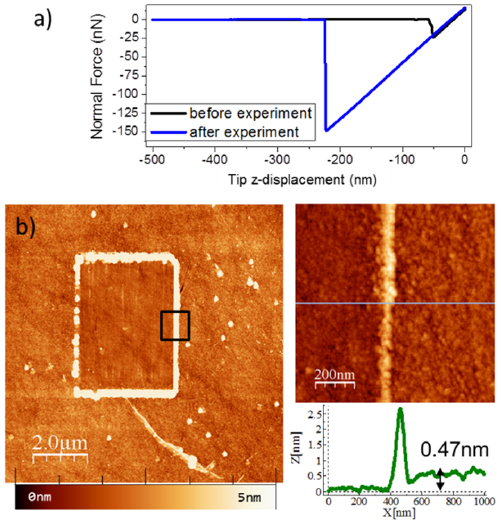
Figure IX.18. (a) Force versus distance curves acquired before (black) and after (blue) sweeping. Only the retract branch is plotted to better visualize the increase in the adhesion force. (b) Topographic image showing the rectangular area with SLG removed. From line profiles taken across the edge, the thickness can be obtained as in as pointed out scanning the inset in (b).
Download figure:
Standard image High-resolution imageDepending on applied force, the material swept by the tip can be either the contaminant layer adsorbed on SLG exposed to air, if forces are restricted to few nN, or the complete layer for forces up to hundreds nN.
KPM can give information on thickness, layer-dependent distribution of charges, electrical potential and work function [1462]. Measurements are performed in dynamic mode, using the amplitude as feedback channel for topographic determination, and the retrace mode for surface potential acquisition, at a lift distance between 15–20 nm. NT-KP tips from Next-Tip S.L. provide very good resolution for KPM [1463].
Surface potential maps can be used to discriminate between N, figure IX.19, for graphene grown on SiC. While the topography image (figure IX.19(a) top) is dominated by SiC terraces, a contrast is observed at the step bunches in surface potential images (figure IX.19(a) bottom), a fingerprint of the presence of BLG [1462, 1464]. The dark contrast corresponds to SLG and the brighter contrast areas, at the step bunches, indicate BLG. Small islands (300–500 nm in diameter) decorating the terraces are assigned to BLG from their contrast. This contrast observed in surface potential as a function of N is ascribed to different work function values for different N, due to different substrate induced doping and different energy dispersions of SLG and BLG [749, 1465, 1466].

Figure IX.19. Simultaneous topographic (top) and surface potential (bottom) images acquired on graphene on SiC. (a) Measurements performed after sample growth. (b) After several days, with the sample kept in ambient conditions.
Download figure:
Standard image High-resolution imageWhen measuring in ambient conditions, aging of the sample can affect the contrast in surface potential. This is shown in figure IX.19(b), where the same sample is measured after growth and several days later. In addition to the presence of small clusters (2–5 nm high) in the topographic image, due to adsorbates, the corresponding surface potential image shows negligible contrast between terraces and steps bunches. This is due to the passivation layer that screens any electrostatic difference between SLG and BLG areas. Annealing in controlled atmosphere above 150 °C is enough to recover the original KPM signal.
KPM was also employed to investigate the changes in work function upon controlled doping [1377]. By definition, the measured surface potential (VSP) is related to the work function (ΦS) [1467] as:

where ΦT is the work function of the tip, and e is the electron charge. Therefore, changes VSP potential for differently doped samples reflect changes in ΦS. The critical point in these studies is ensuring that the tip conditions (particularly, ΦT) do not change. To monitor this, a reference sample of known ΦS (i.e. HOPG, Au) is measured between samples.
To preserve tip conditions, these comparative studies can be done using Kelvin probe force spectroscopy (KPFS) instead imaging acquisition [1468, 1469]. KPFS consists of applying a varying DC bias, to the tip, located above a single spatial location, while monitoring the dynamic response of the cantilever using heterodyne detection [1469]. The force-voltage or frequency-voltage (depending on the detection mode used [1457]) curves have parabolic voltage dependence, and the position of the maximum of the fitted parabola yields VSP. Two representative curves are shown in figure IX.20(a), for SLG doped with Au NPs, for different NP concentration [1377]. The difference in the maximum position of the curves corresponds to a difference in the EF[1377]. For comparison, several curves are acquired on different locations, and measurements are repeated altering the sample order, to ensure reproducibility of measured differences in surface potential. Similar curves are measured in the reference sample after each round. Figure IX.20(b) compares the results of gradual doping with Au NPs, reflected in a gradual variation of the surface potential measured by KPM [1377].
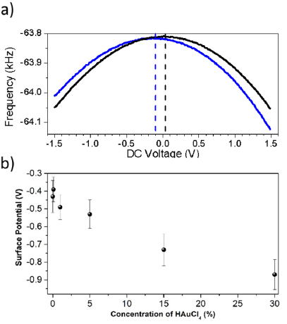
Figure IX.20. (a) Frequency versus voltage curves acquired on SLG on SiO2 doped with HAuCl4 for two concentrations [1377]. VSP corresponds to the maximum of the parabolas, marked with dashed vertical lines. (b) The variation of the measured VSP reflects the tuning of EF upon doping with Au NPs nanoparticles. (Reproduced from [1377], with permission from Elsevier.)
Download figure:
Standard image High-resolution imageIX.1.3. Transmission electron microscopy
TEM techniques can be used to investigate individual flakes from solutions, measuring their lateral size and thickness, the characterization of their crystal structure and chemical composition. Cross section TEM can also be used to give information about N and their interaction with the substrate [688] (see e.g. figure IV.25(e). Since TEM provides a higher resolution compared with SEM and higher throughput compared with AFM, low resolution TEM is frequently used to analyse the shape and lateral size of LPE GRMs statistically [131, 174, 176, 177, 184–186, 188, 190, 239–242, 244, 1470]. To perform these measurements the dispersion is drop-cast onto a TEM grid. Here, it is important to use dilute dispersions (i.e. optically transparent if the material absorbs in the visible) to avoid reaggregation. For statistical length analysis, the longest dimension is measured and denoted as length and the direction perpendicular is denoted as width [131, 174, 176, 177, 184–186, 188, 190, 239–242, 244, 1470]. Depending on the expected flake size, continuous film grids can be beneficial to avoid small flakes falling through the holes. When drop-casting, the best results are obtained when the grid is placed on a filter paper to wick away access solvent [131, 174, 176, 177, 184–186, 188, 190, 239–242, 244, 1470]. During image acquisition, it is important to adjust the field of view according to flake size. Without size selection, samples can be very polydisperse with lateral sizes ranging from 20 nm-a few µm. This is extremely challenging and requires recording higher magnification images as to not bias the statistics towards larger, more easily discernible flakes in wide-view images. Similar to the AFM statistics, the log-normal shape of the histogram can be used as a guide whether counting/imaging are biased [186, 188, 190]. In such cases, a comparison of the statistically determined mean length from AFM and TEM [186, 188, 190] suggests that ~150 counts are sufficient to obtain robust mean values.
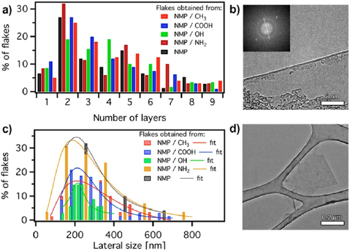
Figure IX.21. TEM analysis of graphene flakes exfoliated in NMP and different Alkanes. (a) Histogram of N. (b) HREM of folded edge. (c) Flake size distribution; data fitted with a log normal function. (d) TEM micrograph of graphene flake. From [235], with permission of The Royal Society of Chemistry.
Download figure:
Standard image High-resolution imageIn addition, thickness determination can be achieved from high-resolution electron microscopy (HREM) images. This is done by counting the number of (0 0 0 2) lattice fringes (see figure IX.21(b)) exposed in folded flakes [235] or by analyzing the electron diffraction pattern intensities from individual crystal [235], providing statistical qualification of the exfoliation process [235]. Additional functional properties can be engineered by decoration with either organic moieties or NPs. In this case, STEM imaging and elemental mapping can provide nanoscale characterization of the decoration and of the interface between NPs and GRMs [235, 288]. Electron beam damage can be limited by reducing the accelerating voltage, making it possible to use TEM for the characterization of blends between GRMs and organic complexes [288].
IX.1.3.1. Low-energy HRTEM
For structural characterization on the atomic level, aberration-corrected high-resolution transmission electron microscopy (HRTEM) is the method of choice. However, for very thin samples such 1L-GRMs, the interactions of energetic electrons with the material during imaging may result in permanent changes in the structure, also referred to as radiation damage. This can be both an obstacle for imaging, as well as a useful tool for manipulating matter at the atomic scales [1471–1474]. The best investigated damage mechanism is the so-called knock-on damage [1475], where the impact of fast electrons gradually removes atoms from the sample. From kinematic considerations [1476], it follows that these alterations can be prevented if a certain threshold energy is undercut [1477]. Depending on the GRM, acceleration voltages of 80 kV and less are required [1478]. At such voltages, in conventional TEMs without aberration correction, atomic resolution is not achievable as the resolution is worse than 0.35 nm already at 80 kV. Today's high-end TEMs are equipped with a corrector for the spherical aberration (Cs), and usually operate at acceleration voltages between 300 kV and 80kV. The resolution is ~0.8 Å at 300 kV and ~1.9 Å at 80 kV, which allows to resolve single atomic columns of many bulk crystalline samples. For SLG, the pristine lattice withstands 80 kV for a sufficiently high electron dose for HRTEM imaging with good signal-to-noise ratio (SNR), however edges and pores will be more quickly altered and much lower voltages are required [1478]. At voltages below 80 kV, the resolving power of Cs-corrected microscopes is however not sufficient as it is limited by the chromatic aberration Cc of the objective lens. In recent years this limitation has been tackled by two approaches: either the effect of chromatic aberration is reduced due to a reduced energy width of the primary electron beam by a cold field emission gun [1479] or by a monochromator (e.g. [1480, 1481]), or, most efficiently, by a chromatic aberration corrector [1482]. Ref. [1482] reported a microscope, the so-called Sub-Angstroem Low-Voltage Electron microscope (SALVE), equipped with a Cc/Cs corrector optimized for voltages between 80 and 20 kV. Even at 20 kV, this microscope can resolve individual C atoms with a resolution < 0.14 nm [1482] over a wide field of view of 4096 × 4096 pixel. With the SALVE microscope, sub-Å resolution resolution is achieved for voltages between 40 kV (0.92 Å) and 80 kV (0.76 Å), and the achievable contrast for the same electron dose is increased [1473, 1484].
Example low-voltage HRTEM images of GRMs are shown in figure IX.22. The diffractograms of SLG and MoS2 (30 kV images) feature reflections up to the third and fourth order. A good agreement between image calculation and experiments can be seen (see linescans A6/B6).
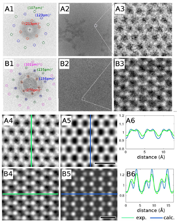
Figure IX.22. Experimental and calculated Cc/Cs-corrected HRTEM images of (A) SLG [1482] and (B) MoS2 at 30 kV. (A1) and (B1) show the Fourier transforms of (A2) and (B2). The outmost reflections demonstrate a resolution ~1 Å. (A3) and (B3) show atomic resolution with magnified areas. The SNR can be improved by averaging the experimental images (A4) and (B4). The results are in good agreement with simulated HRTEM images (A5) and (B5) [1483]. The line scans (A6) and (B6) show the intensity profiles along the marked lines in the experimental and the simulated images. Adapted from [1482], copyright by the American Physical Society.
Download figure:
Standard image High-resolution imageThe tunable low acceleration voltage allows for its optimal choice for each sample. The chosen one is a compromise between the resolving power (which is higher at higher voltages) and knock-on damage. In addition, especially non-conducting material, suffer from ionization effects, which usually increase at lower voltages [1473, 1484]. Sophisticated sample preparation methods are then needed to reduce these effects. The following techniques provide good results: the production of clean surfaces [1485], sandwiching the radiation-sensitive material between two SLGs [1486], and isotope substitution [1487]. To summarize, the choice of the acceleration voltage depends on the trade-off between resolution, knock-on damage and ionization. Appropriate sample preparation is crucial for reaching the voltage-dependent resolution limits. The Cc/Cs-corrected technology for TEM is regarded as a major improvement of the current technology which can be judged from the single-shot images of SLG in figure IX.23, at 80 and 30 kV from the new (Cc/Cs) technology compared with the old (Cs) technology (all single-shot images). Reliable information from HRTEM images about pore sizes distributions in GRMs, or edge structures can now be obtained at lower voltages with higher resolution and higher contrast [1482]. In addition, due to the wide field of view of 4096 × 4096 pixels, this microscope is also very useful for dynamic studies and manipulations at the atomic scale.
Figure IX.23. SLG HRTEM images obtained at 30 kV (left) and 80 kV (middle) in the Cc/Cs-corrected SALVE microscope and at 80 kV (right) in the Cs-corrected TITAN-microscope. The inserts show the corresponding Fourier transform patterns. The (
 2 0), (0
  2 0) and (1
  2 0) reflections are encircled in red, blue, green, and purple, respectively. Adapted from [1482], copyright by the American Physical Society.
Download figure:
Standard image High-resolution imageIX.1.4. STM
STM is a powerful tool for graphene characterization. It is generally used inside UHV chambers for in situ structural and electronic studies at the atomic level. When the graphene samples are measured in ambient conditions or after ex situ manipulations, AFM is a preferred tool as force maps are more directly interpreted in terms of topographic features of the sample. STM images, in contrast, are proportional to the tunnel current which is sensitive to the electronic structure of the tip and surface [1488, 1489]. When samples are characterized in ambient conditions, data acquisition can be quite difficult as atmospheric contaminants may intrude between tip and surface as they diffuse, thus provoking current instabilities and hindering high-quality data acquisition. After graphene exposure to ambient conditions, annealing in vacuum for a short period of time at ~ 250 °C before measurement is recommended in order to remove possible adventitious adsorbates. With respect to the acquisition mode, topography images at constant current are preferred as they are typically more stable and avoid tip crashes during measurements. Nevertheless, the use of constant-height or current-error images can also be useful in some cases for obtaining atomically-resolved images of local features [1490, 1491].
The atomic lattice of graphene can routinely be resolved with STM. A hexagonal lattice with a periodicity of 2.44 Å is normally observed for graphene and graphite samples. When imaging graphene, the smaller periodicity (1.42 Å) of the honeycomb lattice can sometimes also be resolved. Low voltages and high currents (short tip-sample distances) are recommended for obtaining atomic resolution images, with typical values ranging between 50–200 mV and 1–4 nA, respectively. Graphene superlattices of larger scale (1–2 nm) can also be resolved with STM images STM is the ideal tool for local measurements needing ultrahigh spatial resolution. STM has demonstrated its capabilities for resolving low-dimensional structural defects with unmatched atomic resolution. There are several defective structures that have been described by STM images. The most important 1d defective structures are wrinkles and graphene edges between different (rotational) domains. Figure IX.24 shows a representative STM image of a graphene on Pt(1 1 1) sample together with a representative LEED pattern of the same system [1035]. In the constant-current topographic image, a graphene pleat and some graphene nanobubbles can be seen. Profiles along this pleat show an apparent height ~ 2–2.5 nm. The origin of these structures is the difference between thermal expansion coefficients of graphene and Pt, which results in compressive strain during cooling. Graphene nanoscale dome-like structures, also known as nanobubbles, can also be resolved with STM images. In figure IX.24(a) one is encircled in yellow and in figure IX.24(b) one is shown with atomic resolution. Structures submitted to compressive strain, like graphene pleats and nanobubbles, have been proposed to induce high pseudo-magnetic fields, which lead to Landau quantization of the electrons when measured with STM at cryogenic T [632].

Figure IX.24. (a) STM image of a 200 × 200 nm2 area of graphene grown on Pt(1 1 1), I = 0.15 nA, V = 750 mV. A SLG covers the whole surface. In the image a wrinkle/pleat and several nanobubbles, one of them is encircled in yelow, can be seen. The inset shows the characteristic LEED pattern of SLG on Pt(1 1 1). (b) High resolution STM image of a graphene nanobubble (20 × 20 nm2, I = 0.6 nA, V = 310 mV) and few point-like atomic defects with atomic resolution. Figure a is adapted from [1035], with permission from Elsevier.
Download figure:
Standard image High-resolution imageIn figure IX.25 different point defects of a SLG/Pt(1 1 1) system are depicted. Figure IX.25(a) shows a single atom defect which can be explained in terms of an in-lattice heteroatom inclusion,–most likely a N impurity coming from the residual gas in the chamber [1492] Figure IX.25(b) displays a multiatomic vacancy which induced a reconstruction of a region ~ 1–2 nm. Although a dome-like local configuration can be expected one must take with caution the fact that this region appears brighter, thus higher, in the STM images as electronic effects are normally occurring in the defective regions of graphene. Figure IX.25(c) shows a strain-induced lattice dislocation involving at least two unit cells of graphene.
Figure IX.25. 5 × 5 nm2 images showing graphene point defects on Pt(1 1 1). (a) 10 mV, 3.9 nA. (b) 10 mV, 2 nA. (c) 10 mV, 3.9 nA.
Download figure:
Standard image High-resolution imageIX.1.4.1. Graphene on metals
The formation of graphene has been mostly studied by STM on hexagonal metal surfaces, like the (0 0 0 1) for the HCP crystallographic structures, Ru, Co, Re, and the (1 1 1) for the FCC metals, Ni, Cu, Rh, Pd, Ir, Pt and Au, but it has also been observed to grow on non-hexagonal crystallographic surfaces such as Pt(1 0 0) [1031].
Moiré superstructures [902] arise from the electronic interference between two periodicities with a difference in lattice parameter and/or angle. In the present case moirés are originated by the interference between graphene lattice and metal surface beneath it. Figure IX.26 shows a ball and stick model of a moiré pattern for describing the different distances and angles occurring in moiré superstructures. With these parameters, models minimizing lattice mismatch can be used for describing the structure of graphene with respect to the metal substrate. Figure IX.27 presents the STM images of four moiré superstructures on SLG/Pt(1 1 1) that can be described with these structural parameters (see blue hexagons overlaid onto it). In every STM image, two periodicities can be seen: a short one, corresponding to atomic resolution, and a long one, corresponding to the moiré superstructure.
Figure IX.26. Diagram of the model represented for a moiré superstructure. Pt atoms are represented by blue spheres, whereas the hexagonal lattice of graphene is represented by black spheres. The angle between the black dotted line and the Pt ![$\left[ 1\,\overline{1}\,0 \right]$](https://content.cld.iop.org/journals/2053-1583/7/2/022001/revision1/tdmab1e0aieqn070.gif) surface direction (x axis) represents the crystallographic angle, Φ = 25.1° for this case. The orange spheres are C atoms with the lowest mismatch for a given Φ, which define the moiré unit cell indicated by the black rhombus. The angle between the orange dashed line and the Pt
surface direction (x axis) represents the crystallographic angle, Φ = 25.1° for this case. The orange spheres are C atoms with the lowest mismatch for a given Φ, which define the moiré unit cell indicated by the black rhombus. The angle between the orange dashed line and the Pt ![$\left[ 1\,\overline{1}\,0 \right]$](https://content.cld.iop.org/journals/2053-1583/7/2/022001/revision1/tdmab1e0aieqn071.gif) direction is the moiré apparent angle (Ω). The white arrow in the inset represents the mismatch. Adapted from [902], copyright American Chemical Society.
direction is the moiré apparent angle (Ω). The white arrow in the inset represents the mismatch. Adapted from [902], copyright American Chemical Society.
Download figure:
Standard image High-resolution image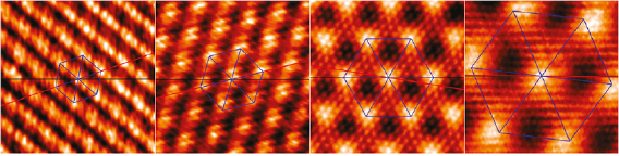
Figure IX.27. High resolution atomically resolved STM images of periodically modulated graphene structures. The red line indicates the graphene orientation with respect to the black line, which indicates the Pt [1 1 0] surface direction. The blue hexagon denotes the resulting moiré structure. All images are 5 × 5 nm2. V ~ −250, +250 mV; I ~ 1, 3 nA. Adapted from [902], copyright American Chemical Society.
Download figure:
Standard image High-resolution imageDepending on the reactivity of the metal, the interaction between graphene and metal substrate can range from van der Waals physisorption to strong bonded chemisorption. The interaction between substrate and graphene overlayer drives the measured STM corrugation and the mean distance from the substrate [901]. Typical corrugations of moiré supperlattices range between 0.2–1.2 Å for graphene grown on metal surfaces, and typical corrugations for the atomic lattice range between 0.1–0.3 Å [901].
Figure IX.28 presents a series of defective structures appearing on the SLG/Pt(1 1 1). This figure shows how graphene adjusts itself to the lowest energy conformation when grown on surfaces, thus deforming its atomic structure to fit to the substrate and other graphene grains in the vicinities. Figure IX.28(a) shows two moiré domains lying in the same Pt(1 1 1) terrace, connected by an amorphous grain boundary. The strain accumulated between the two domains induces the appearance of an edge. Figure IX.28(b) shows that graphene can, in some cases, run across an atomic step without forming a grain boundary in a 'carpet-like' fashion (covering unperturbed the higher and lower part of the step while running through it). In this case the only effect is an out-of-plane bending of SLG. In figure IX.28(c) a pseudo-periodic graphene grain boundary is presented. The structure involves several, unresolved, vacancies and lattice deformations. Interestingly, in cases like this, the grain boundary can be pseudocrystalline (contrary to figure IX.28(a)) and adopt the periodicity of one of the two moirés that reaches the interface.
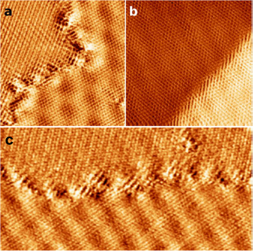
Figure IX.28. Examples of defective structures of graphene. (a) edge between two rotational domains (moirés) 10 × 10 nm2 1.9 nA, 10 mV. (b) Graphene running through a Pt step in a carpetlike fashion 7.5 × 7.5 nm2, 8 nA, 2 mV. (c) Pseudo periodic edge, the grain boundary follows the periodicity of the moiré appearing in the lower part of the image. 18.4 × 9 nm2, 2 nA, 10 mV.
Download figure:
Standard image High-resolution imageFigure IX.29 presents a different 1d structure occurring on graphene on metals: the interface between graphene and a metal step (in particular a Pt(1 1 1) surface). In this case a crystalline structure emerges permitting to perform a combined experimental-theoretical approach to study the contact region formed along the interface at the atomic scale. Figure IX.29(a) shows a high-resolution STM image of atomically resolved border-like edge of (√7 × √7)R19° graphene with a Pt(1 1 1) step. Combining STM images with DFT simulations, the atomic and electronic structure of Pt-graphene edges can be fully characterized (see figure IX.29(b)). This approach reveals electronic highly localized states in one of the graphene sublattices, and thus the brighter aspect in the STM images of the contact region. Theory predicts, and STM images confirm, that this state is mainly confined on the first C atomic lines of the edge [1590].
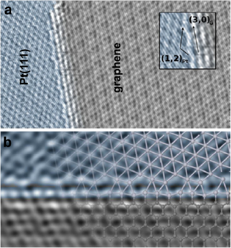
Figure IX.29. Graphene-metal interface. (a) High resolution, atomically resolved, STM images of SLG/Pt(1 1 1)-Pt(1 1 1) interface. These crystalline edges are energetically favoured and have the same orientation as the graphene moiré superstructures. 12.6 × 6.8 nm2, V = 40.2 mV, I = 5.2 nA. The inset shows the chiral vectors of this particular edge. (b) Ball and stick model of the DFT relaxed structure (right-hand part of the image) compared with the STM image of the SLG-Pt(1 1 1) edge boundary. The atomic positions of the calculations reproduce with great accuracy the protrusions in the STM images. Adapted from [1490], copyright American Chemical Society.
Download figure:
Standard image High-resolution imageIX.1.4.2. Silicon carbide
Graphene grown on SiC(0 0 0 1) shows very interesting electronic properties at the nanoscale. When inspected with STM, it can appear transparent, depending on the bias voltage. Used: The honeycomb graphene structure is 'visible' only within a small range of scanning conditions which typically involve voltages bias near EF (see figure IX.30) [659]. SLG/SiC(0 0 0 1) present quantum interferences between electrons of different sublattices, which result in a √3 × √3R30° lattice appearance of graphene lattice near defective structures. All these characteristics makes G/SiC(0 0 0 1) an ideal system to test the fundamental electronic properties of this pure sp2 compound with STM, although typically low T STM is needed to decrease electronic broadening effects. The, so called, C-terminated SiC face or SiC(0 0 0  ) develops MLG. Its layers are weakly bound and stacked in different orientations forming graphene-graphene moirés with different orientations and periodicities [600, 659].
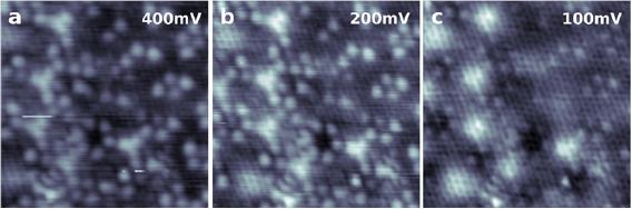
Figure IX.30. STM images of the same region showing the bias dependence of SLG/SiC(0 0 0 1). When scanned at bias near EF (100 mV) the main feature is the graphene lattice, while scanned at higher bias (400 mV) the subsurface buffer layer structure is revealed. 7 × 7 nm2.
Download figure:
Standard image High-resolution imageGraphene grown on the Si terminated surface SiC(0 0 0 1) can show different surface reconstructions (see section IV). There are three main surface terminations that can be distinguished by STM. First, (6 √ 3 × 6 √ 3)R30°/SiC(0 0 0 1) or buffer layer (figure IX.31(a)) is a carbon rich termination which is usually described as sp2 carbon lattice covalently bound to the uppermost SiC slab. Second, SLG, figure IX.31(b), is characterized by a (6 √ 3 × 6 √ 3)R30° superperiodicity overlaid with an atomic scale graphene lattice. When measuring SLG at high voltage bias one can normally measure the atomic features of the SiC beneath graphene [1493]. Third, BLG and, more generally, MLG. When SiC samples are annealed at very high T, Si depletion can be high and promote MLG growth. STM measurements of MLG (figure IX.31(c)) have lower corrugation and, in some cases, the underlying superperiodicity disappears and a graphene–graphene moiré superlattice dominates. Similar MLG are also found in the SiC(0 0 0 − 1) surface [1494]. SLG can be decoupled from the SiC substrate by H intercalation. Figure IX.31(d) shows a STM image of hydrogen intercalated graphene. In this case, the underlying (6 √ 3 × 6 √ 3)R30° superperiodicity is not appearing in the STM images and only the graphene lattice can be resolved. The low surface corrugation measured with STM on the hydrogen intercalated samples might be related to the high µ reported for these samples.
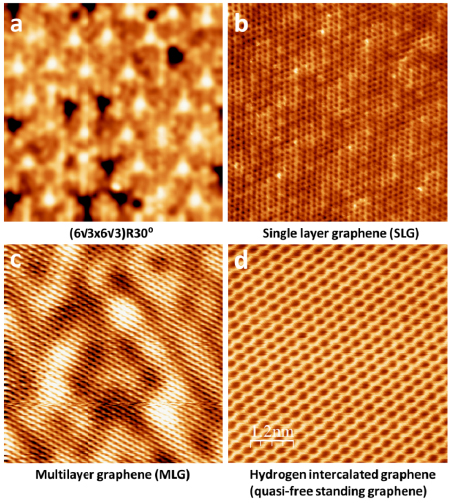
Figure IX.31. Atomically resolved STM images of the SiC surface with different terminations. (a) 6 √ 3 × 6 √ 3)R30°1000 mV, 200 pA. (b) SLG −100 mV, 200 pA. (c) MLG, −100 mV, 100 pA. (d) Hydrogen intercalated graphene. V = 243 mv; I = 1.33 nA. Images (a)–(c) are 10 × 10 nm2. d is 6 × 6 nm2.
Download figure:
Standard image High-resolution imageThe (0 0 0 −1) face shows ordered graphene over mm scales, easily observed by STM on doped SiC. This allows atomic moiré and spectroscopic studies at low T and high magnetic field [595, 600, 627, 630].
IX.1.5. Scanning thermal microscopy
Heat transfer properties of graphene are a topic of high interest [1495–1498] based on calculations and measurements of its thermal conductivity in the range of a few thousands W/mK [1499]. Due to the strong covalent sp2 bonding, heat transport in carbon materials is usually dominated by phonons [1498]. However, lattice defects, impurities, interfaces as well as the presence of sp3 bonds can limit heat conduction [1498]. Several techniques have been proposed for characterizing the GRM thermal properties [1500]. However, accurate and reliable measurements remain challenging. Electrical methods and the Raman optothermal measurements were used to determine the thermal conductivity of both suspended and supported SLG [1498, 1501, 1502]. The main limitations are the rather complex setup and limited spatial resolution. Optical techniques are limited to a few hundreds nm by the diffraction limit of the incident light, while electrical measurements provide a result representing the average of the conductivity on the whole specimen.
Scanning thermal microscopy (SThM) [1503, 1504] is an interesting technique to measure heat transfer in GRMs, requiring limited sample preparation and with lateral resolution of some tens nm or less. Although a quantitative determination of the thermal conductivity of GRMs by SThM [334, 1504] is very challenging, it was demonstrated to be possible in at least some specific cases and with particular probes, e.g. by electrically heating a suspended SLG and by using the so called null point technique, adopting probes integrated with a thermocouple junction [1505].
SThM can be performed by using resistive probes, where a Pd film acts both as heater and T sensor (the so-called Pd probes) [1504]. A 40 nm [1506] Pd film, deposited near the apex of the Si3N4 tip, acts as the element of a Wheatstone bridge. The resistor is heated by Joule effect and, when the tip is in contact with more thermally conducting regions of the sample, its T (and therefore resistance) decreases, while it increases when scanning on less conductive areas, since less heat is carried away by the material under investigation. The change in the sensor resistance is monitored by measuring the bridge voltage, which is sent to the controller to display the thermal maps, subsequently converted into T by using the Wheatstone bridge formula [1789], and the temperature coefficient of the probe ~ [1790]
RGO flakes were studied by SThM [334]. These were measured both 'as-received' (RGO) or after a annealing at 1700 °C in vacuum for 1 h (referred to as RGO_1700) to gain insight into the evolution of the heat dissipation properties, due to the simultaneous reduction of disorder and defectiveness upon annealing [334]. SEM and AFM analyses did not evidence significant changes in the morphology upon annealing. XPS showed a strong reduction of oxygen, by the elimination of carboxylic and carbonyl groups. A considerable reduction of defects was observed by Raman spectroscopy which also indicated an increase of the graphitic stacking order [334]. This result was further confirmed by x-ray diffraction experiments which revealed an increased ordering both along and perpendicular to the planes. Figure IX.32 plots the SThM maps for (a) RGO and (b) RGO_1700 on Si/SiO2. Topography artefacts are observable owing to the dependence of the tip-sample contact on steep edges, wrinkles and bulges on the surface [334, 1507]. The tip heater T in panel (a) shows that on the flat areas of the sample (see e.g. the masked region), T is basically the same as when the tip is scanning the substrate ( ). This does not mean that the two materials have the same thermal conductivity, but only that their apparent thermal conductance is the same. On the other hand, in panel (b) it can seen that for the annealed flakes T is now lower when the tip is on the flake than when it is on the substrate,
  . Thus, by comparing (a) and (b), Ref. [334] concluded that the annealed flake features a higher thermal conductivity than the as-received ones, due to the reduced disorder and defectiveness upon annealing. Panel (c) and (d) show an analogous result, but with the flakes supported by the less (one order of magnitude) thermally conducting PET. In this case, the heater T on the RGO flake is now lower than that of the substrate (
 ) and also in this case
  increases when looking at the RGO_1700 sample, where it goes to
  . The results on PET confirm that RGO_1700 flakes are more thermally conducting and also show that the use of a less conducting substrate enhances the sensitivity of the measurement. This is due to the decrease of spreading resistance [1508] of the substrate occuring when enlarging the heat flow area, being larger when the thermal conductivity of the substrate is smaller [334]. Thus, the T difference substrate-flake is also expected to be higher.
Figure IX.32. SThM maps of (a) RGO and (b) RGO_1700 on Si/SiO2 and (c) RGO and (d) RGO_1700 on PET. Adapted from [334], with permission from Elsevier.
Download figure:
Standard image High-resolution imageFigure IX.33 reports a summary of the SThM results obtained in terms of T differences between substrate and flakes for several samples on substrates. Although these are small and the error bars rather large, the result is reproducible on both substrates, showing that the annealing process improves the thermal conduction of flakes. No particular dependence on flake thickness of the flakes is observed, likely due to the fact that the in-plane component of the thermal conductivity is at least two orders of magnitude higher than the out-of-plane one, and a considerable amount of heat could be spread along the planes.
Figure IX.33. (a) Summary of T difference between Si/SiO2 and RGO (red) or RGO_1700 (blue). (b) The same as in (a) but for PET substrate. Adapted from [334], with permission from Elsevier.
Download figure:
Standard image High-resolution imageSThM was also applied on CVD 4LG, BLG, SLG supported by SiO2/Si (figure IX.34). Figure IX.34(a) shows a thermal map os SLG on SiO2/Si. The high-T spots are due to impurities and the corresponding T value is due to a topography artefact [1507]. When averaging over the flat areas (with no topography artefacts) the measured tip T is lower than on the substrate. By averaging the red masked area on one 1LG and on a similar area on the substrate (not shown), the T difference between substrate and sample was found to be  [1790]. Figure IX.34(b) reports a similar image for 2LG. Apart from topological features giving rise to high-T spots, the flat areas of the surface feature on average a lower T than the substrate, with a T difference (averaged on the red masked area) increased to
  , suggesting that 2LG has a higher thermal conductance than 1LG. Figure IX.34(c) shows the 4LG case, in which both impurities and grain boundaries are visible due to the topography-related T readings. The representative T on the sample flat areas is much lower than on the substrate. The T difference between substrate and 4LG is now higher than for the two previous samples.
  , indicating that the thermal conductance of 4LG is further increased with respect to 1LG and 2LG. Figure IX.34(d) summarizes the results obtained by performing several SThM measurements as a function of N. Even though the error bars for 1 and 2LG overlap, the thermal conductance increases with N.
Figure IX.34. SThM maps of (a) 1LG, (b) 2LG, and (c) 4LG, on Si/SiO2. (d) Sensor T difference as a function of N. The dashed line is a guide for the eye.
Download figure:
Standard image High-resolution imageA similar trend was reported for mechanically exfoliated flakes using either the resistive Si [1509] or Pd probes [1506]. The topography of CVD graphene, with grain boundaries and crystallites, is considerably different from mechanically exfoliated flakes, that are much flatter and more regular. This affects also the heat dissipation properties and the thermal response of the SThM probe.
IX.2. Spectroscopies
IX.2.1. Raman
Raman spectroscopy is an integral part of graphene research. It may be used to determine the number and orientation of layers, the quality and types of edge, and the effects of perturbations, such as electric and magnetic fields, strain, doping, disorder an functional groups [96].
This, in turn, provides insight into all sp2-bonded carbon allotropes, because graphene is their fundamental building block. Ref. [96] reviewed the state of the art, future directions and open questions in Raman spectroscopy of graphene. It described the key physical processes, such as the various types of resonances at play, and the role of quantum interference. It outlined the basic concepts and notations, and a terminology able to describe any result in literature for GRMs. Here we briefly describe some of the key concepts, referring the reader to Ref. [96] for a more complete overview.
An ideal characterization tool should be fast and non-destructive, offer high resolution, give structural and electronic information, and be applicable at both laboratory and mass-production scales. Raman spectroscopy fulfils all these requirements. The Raman spectrum of graphite was first recorded 50 years ago [1510] and, by the time the Raman spectrum of graphene was first measured [105], Raman spectroscopy had become one of the most popular techniques for the characterization of disordered and amorphous carbons, fullerenes, nanotubes, diamonds, carbon chains and polyconjugated molecules [1511]. Raman techniques are particularly useful for graphene, because the absence of a bandgap makes all wavelengths of incident radiation resonant, thus the Raman spectrum contains information about both atomic structure and electronic properties. Resonance could also be reached by ultraviolet excitation [1722] either with the M-point Van Hove singularity or in the case of bandgap opening, such as in fluorinated graphene.
Raman spectra are typically measured in the high frequency range >100 cm−1 because of the cut-off limit of Raman filters (edge or notch filters). In the low frequency (<100 cm−1) range interlayer interaction can be estimated by the shear (C) and layer breathing modes (LBMs), which can also be used to determine N [1514, 1515]. Traditionally, a triple stage spectrometer is used to measure low frequency Raman spectra, but its low throughput and complexity for operation restrictsed its utilization. A new method was developed to get low frequency spectra easily, using volume Bragg grating filters to reject a strong laser line down to 5 cm−1 [1516, 1514]. When measuring GRMs, the damage threshold for the laser power should be considered. Typically, the power should be kept <1 mW for SLG, and few hundreds µW for TMDs, depending on the material. Some materials should be isolated from air with a protection layer or vacuum to avoid photo induced oxidation [189].
IX.2.1.1. Graphene
A typical Raman spectrum of defect-free SLG consists of two main peaks, the G peak located at ~1580 cm−1 and the 2D peak at ~2700 cm−1 [96], figure IX.35. In defective graphene, additional peaks such as the D, D' and their combination D + D' appear [96, 1511, 1524, 1722], figure IX.35 bottom spectrum. 2D and 2D' are second order peaks involving two phonons and are thus always present even in the absence of defects. The fitting parameters, such as peak position Pos, FWHM, height (I) and area (A) are important to interpret Raman data. E.g.: I(G) for G peak height, A(G) for G peak area, Pos(G) for G peak position and FWHM(G) for G peak full-width at half-maximum.
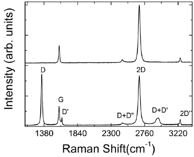
Figure IX.35. Typical Raman spectra of defect free (top) and defective (bottom) graphene. Figure taken from [96], with permission of Springer.
Download figure:
Standard image High-resolution imageThe lineshape of the 2D peak can be used to distinguish between different N. For SLG it can be fitted with a single Lorentzian, while in BLG it splits into four components as result of the evolution of the band structure [105]. For N > 10 the 2D peak shape is similar to that of graphite. For graphene on the carbon (0 0 0 − 1)face of SiC, each layer has the electronic structure of a single layer, due to the rotational stacking, and the Raman 2D peak is a single Lorentzian in most cases [1517], see figure IV.7(b). The C and LBMs can be observed for GRMs. Their positions change with N. They can also be used to calculate coupling constants related to in-plane and out-of-plane Young's moduli [1514]. Figure IX.36(b)) shows the low frequency Raman spectra of different graphene layers. While Pos(G) is nearly constant, Pos(C) changes and can be used to determine N.
Figure IX.36. (a) Raman spectrum of 2D peak as function of N [78]. (b) and G peaks as function of N. (c) Pos(C) and Pos(G) as a function of 1/N [1514].
Download figure:
Standard image High-resolution imageRaman spectroscopy can also be used to determine the doping level [1321, 1518, 1519]. There are two major effects: (i) a change of the equilibrium lattice parameter with a consequent stiffening/softening of the phonons, and (ii) the onset of effects beyond the adiabatic Born–Oppenheimer approximation that modify the phonon dispersion close to the Kohn anomalies (KA) [1518, 1520].
In doped samples Pos(G) increases, while FWHM(G) decreases for both electron or hole doping [1518, 1521–1523]. The increase in Pos(G) is due to the non-adiabatic KA removal, while the decrease in FWHM(G) is due to Pauli blocking of the phonon decay channel into electron hole pairs due to the increase in EF [1522, 1518]. The 2D peak instead shifts up for hole doping and down for electron doping, due to the change of the equilibrium lattice parameter. Therefore, Pos(2D) can be used to determine the type of doping. Doping also has an effect on I(2D)/I(G) and A(2D)/A(G). Both are maximum for zero doping and decrease for increasing doping [1522, 1518]. Figure IX.37 summarizes the doping dependence of all the fitting parameters. Using Pos(2D) one can distinguish between electron and hole doping, and then use all the remaining fitting parameters and Pos(2D) to estimate the amount of doping. The charge carrier concentration is related to the Fermi level by [1518]: EF(n) = ħ|vF| √ (π n), where ħ = h/2π is the reduced Planck constant, vF = 1.1 * 106 m s−1 is the SLG Fermi velocity
Figure IX.37. Doping dependence of Raman fitting parameters (a) Pos(G), (b) FWHM(G), (c) Pos(2D), (d) I(2D)/I(G) versus electron concentration (×1013 cm−2) and (e) [A(2D)/A(G)]0.5 as a function of EF. Adapted from Ref. [1518], with permission of Springer and from Ref. [1519], copyright by the American Physical Society.
Download figure:
Standard image High-resolution imageRef. [1524] introduced a three-stage classification of disorder, leading from graphite to amorphous carbons, that allows to simply assess all the Raman spectra of carbons:
- Stage 1: graphene to nanocrystalline graphene.
- Stage 2: nanocrystalline graphene to low-sp3 amorphous carbon.
- Stage 3: low-sp3 amorphous carbon to high-sp3 amorphous carbon.
Here we focus on stage 1, the most relevant when considering the vast majority of publications dealing with graphene production, processing and applications. As shown in figure IX.38, in stage 1 the Raman spectrum evolves as follows: (a) the D peak appears, I(D)/I(G) increases; (b) the D' peak appears; (c) all peaks broaden; (d) the D + D' peak appears; (e) at the end of stage 1, the G and D' peaks are so wide that it is sometimes more convenient to consider them as a single, up-shifted, wide G band at ~1600 cm−1 [1524].
Figure IX.38. Representative Raman spectra of ion bombarded SLG measured at EL = 2.41 eV [1322].
Download figure:
Standard image High-resolution imageFor a sample with rare defects I(D) is proportional to the total number of point defects probed by the laser spot, giving rise to I(D)/I(G) ~ 1/ , where LD is the average inter-defect distance. Taking into account the excitation energy dependence of the peak areas and intensities the inter-defect distance can be expressed by [1322, 1524]:
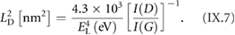
EL is the laser excitation energy in eV. This relation is valid for LD ⩾ 10 nm (stage 1). By considering point-like defects, separated from each other by LD, equation (IX.7) can be restated in terms of defect density, nD, given by  , as [1322]:
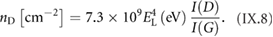
Equations (IX.7) and (IX.8) are limited to Raman-active defects. Perfect zig-zag edges [1526], charged impurities [1518, 1527], intercalants [1528], uniaxial and biaxial strain [1275, 1529–1534] do not generate a D peak.
Equations (IX.7) and (IX.8) are derived assuming negligible EF shift. However, most samples in literature show doping levels ~200–500 meV. I(D) depends on the doping level [1321]: I(D) decreases for increasing doping. This needs to be taken into account when estimating the defect density. Equations (IX.7) and (IX.8) can be modified for samples with non-negligible doping [1321]:
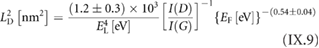
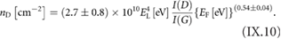
Equations (IX.9) and (IX.10) are valid for samples with a defect concentration corresponding to stage 1, and for EF < EL/2, which is by far the most relevant for graphene production and applications.
In order to extract the defect density correctly the flowchart presented in figure IX.39 should be followed.
Figure IX.39. Flowchart to estimate defect density in doped and undoped samples.
Download figure:
Standard image High-resolution imageAfter recording a Raman spectrum, one first has to check whether a D peak is present. In case no D peak is present, the standard procedure of estimating doping from the Raman fitting parameters, such as Pos(G), FWHM(G), Pos(2D), I(2D)/I(G) and A(2D)/A(G), can be used. The presence of a D peak, leads to the next step, where one needs to check if the sample is doped or not, e.g. by looking at the relevant Raman peak fitting parameters. If the sample has doping ⩽100 meV, equation (IX.8), can be used to estimate the defect density. If however the sample has non-negligible dopingequation (IX.10) has to be used. E.g. Figure IX.40 shows spectra of a defective SLG at low, EF = 100 meV, and high, EF ~ 500 meV, doping. By analysing the spectra of doped and defected SLG (black line in figure IX.40) Pos(G) = 1599 cm−1, FWHM(G) = 12 cm−1 and I(2D)/I(G) = 0.94 are obtained. This allows us to estimate ~500 meV for the doping level of the sample using the graphs from Ref. [1518]. The 2D peak is upshifted with Pos(2D) = 2651 cm−1 suggesting hole doping. A decrease of I(D) with doping is seen. The red spectrum for the undoped case gives I(D)/I(G) = 2.8. Using equations (IX.7) and (IX.8) gives nD ~ 3.1 × 1011 cm−2 LD = 10 nm. The black line gives I(D)/I(G) ~ 1.24. Taking the doping level ~500 meV into account nD = 3.4 × 1011 cm−1 and LD = 10 nm, are obtained using equations (IX.9) and (IX.10).

Figure IX.40. Raman spectra of a defective graphene sample (a) EF ⩽ 100 meV and (b) EF ~ 500 meV. Excitation wavelength: 633 nm. Adapted from [1321], copyright American Chemical Society.
Download figure:
Standard image High-resolution imageStrain can be present in a material compressed or stretched out of equilibrium. Strain can be either compressive or tensile. While compressive strain causes an upshift or stiffening of the Raman peaks, tensile strain causes a downshift or softening. Strain can be either isotropic, i.e. biaxial strain, or along a certain axis, i.e. uniaxial. Biaxial strain does not cause any change in peak shape, while uniaxial strain causes splitting of the G peak into two components G+ and G− for ε ⩾ 0.5% [1529], figure IX.41. The G peak is due to a doubly degenerate E2g mode [105]. By applying uniaxial strain this splits into two components, one along the strain direction and one perpendicular to it. While Pos(2D) changes as δPos(2D)/δε ~ −64 cm−1/%, the G peak changes as δPos(G+)/δε ~ −10.8 cm−1/% and δPos(G−)/δε ~ −31.7 cm−1/% [1529] in uniaxial, tensile strain experiments. Ref. [1529] reported δPos(2D)/δε ~ −144 cm−1/% and δPos(G)/δε ~ −58 cm−1/% for biaxial strain. To estimate the strain, the difference between fitted peak positions and unstrained reference peak positions needs to be derived. Then, by knowing how much the peaks shift with strain, i.e. δPos(2D)/δε ~ −64 cm−1/% in case of the 2D peak for uniaxial strain, one can calculate the strain. To distinguish and decouple the combined effects of doping and strain a thorough analysis of all the fitting parameters is necessary [1527].

Figure IX.41. Change in Pos(G) and Pos(2D) with increasing tensile, uniaxial strain. Adapted from [1529], copyright American Chemical Society.
Download figure:
Standard image High-resolution imageIX.2.1.2. HBN
Two Raman peaks in hBN are observed with the excitation of visible laser light, the C peak near 50 cm−1 and a high frequency E2g mode near 1366 cm−1 [1537]. The C peak strongly depends on N so that it can be used to estimate N [1048, 1538, 96]. The high frequency E2g Raman peak weakly depends on N. The peak positions for the mono layer and bulk are ~1368 cm−1 and ~1366 cm−1 [1048, 1539–1541]
IX.2.1.3. Transition metal dichalcogenides
Many TMDs are composed of three atomic layers X–M–X, represented by MX2, as well as ordering, 2H (Hexagonal symmetry), 3R (rhombohedral symmetry) and 1T (tetragonal symmetry).The most common polytype is 2H, e.g., MoS2, MoSe2, WS2, and WSe2. For 2H-MX2, two prominent Raman peaks appear in the high frequency range, A1' and E' modes. A1' is an out-of-plane vibrational mode and E' is an in-plane one [1543, 1544]. The peak positions depend on N so that the difference of their positions may be used to estimate N. However, one needs to be careful since the dielectric environment can also change this difference, for a fixed N. Typically, A1' decreases with decreasing N, and E' has the opposite trend. In the low frequency range, C and LBMs are observed and can be used to estimate the coupling strength between layers and N [96]. Defects in MoS2 broaden the E' and A1' peaks and E' becomes asymmetric towards lower frequencies [1545]. A peak ~ 200 cm−1 appears due to the defect induced longitudinal acoustic (LA) phonon at the M point [1545]. As uniaxial strain increases on 1L-MoS2, the A1' peak shows no measurable shift while the E' peak splits into two, E'+ and E'− [1546]. The E'− peak shifts ~ 4.5 cm−1/% strain and E'+ ~1.0 cm−1/% strain. A1' is not sensitive to strain, while it is sensitive to doping. By increasing doping of 1L-MoS2, A' redshifts and broadens due to electron–phonon interactions [1542].
IX.2.2. Absorbance and fluorescence
IX.2.2.1. Transition metal dichalcogenides
UV/Vis transmission spectroscopy can provide information GRM flakes, as inorganic LMs have well documented excitonic transitions [1547] characteristic for the material and even polytype or phase [378, 379, 1407]. Information on concentration can be extracted [185, 186, 236, 1407, 1548]. However, for this to be performed reliably, one needs to be aware that when transmittance mode is used, extinction and not absorbance spectra are obtained. Extinction is related to transmittance, Tr, via Tr = 10−Ext, where Ext = εcCol, with εc the extinction coefficient, Co the flakes concentration and l as the path length. This means that the quantity that is measured contains information related to both absorbance and scattering of light [185, 188, 190, 236, 240, 1549]. Although the scattering component of the extinction is size dependent [185, 188, 190, 236, 240, 1549], it is also the case that the absorbance coefficient is dependent on size, due to edge effects [185, 186, 188, 190]. Hence, the overall extinction coefficient is size-dependent and it is necessary to determine it gravimetrically for dispersions with a range of lateral sizes and thicknesses to achieve an accurate Co determination.
The change in extinction and absorbance spectra with lateral size can be used to establish metrics for lateral size once the sizes are calibrated by statistical microscopy. Such relationships were established for MoS2 [185], WS2 [186], GaS [188] and black phosphors [190].
Changes in LM band structure as a result of confinement are reflected in changes in peak position of excitonic transitions. This means that information on N is encoded in optical extinction spectra [185, 186, 188].
An example of the spectral changes with size and thickness for LPE MoS2 and WS2 is in figure IX.42 [245]. Figures IX.42(A) and (C) plot optical extinction spectra of MoS2 (A) and WS2 (C) with different mean flake sizes and thicknesses. Due to the power law nonresonant scattering background (>680 nm for MoS2, >650 nm for WS2), peak positions are best found from the second derivative. Second derivative spectra of a subset of the samples in the region of the A-exciton are shown in figures IX.42(B) and (D). Peak intensity ratios can be used to express the changes associated with edge effects. Figures IX.42(E) and (F) plot peak intensity ratios as function of mean flake length for MoS2 and WS2, showing that both materials behave similarly. This means that the flake size for both materials can be quantitatively linked to the length via identical equations [245]. Due to the changes in spectral shape, extinction coefficients are also dependent on size. This is more or less severe depending on spectral position. E.g. as plotted in figure IX.42(G), the extinction coefficient of the A-exciton for both materials is strongly length dependent. However, this is not the case at 345 nm for MoS2 and 235 nm for WS2 so that the extinction coefficient at these spectral positions can be used as a robust measure for Co over a broad range of sizes. In addition, extinction spectra do not only provide insight in lateral size and dispersed concentration, but also in thickness. N can be quantitatively related to the peak position/energy of the A-exciton (obtained from an analysis of the second derivative), as plotted in figure IX.42(H).

Figure IX.42. (A) and (C) Optical extinction spectra of LCC separated MoS2 (A) and WS2 (C). Peaks relevant for the analysis are indicated. (B) and (D) Second derivatives of the A-exciton versus energy for MoS2 (B) and WS2 (D) after smoothing the second derivative with Adjacent Averaging. The solid lines are fits to the second derivative of a Lorentzian to assess peak positions/energies. (E) and (F) peak intensity ratios as a function of 〈L〉. Data for MoS2 and WS2 fall on the same curve. Hence, the same equation can be used to quantify the flakes' length. (E) peak intensity ratio at the A-exciton/local minimum. (F) peak intensity ratio at the high energy maximum/local minimum. (G) Extinction coefficient at different spectral positions as function of flakes' length. At some spectra positions (such as the A-exciton), extinction coefficients are size dependent, while at others (345 nm for MoS2 and 235 nm for WS2) this is not the case. (H) A-exciton peak energies (from second derivatives) as function of 〈N〉. Adapted with permission from [245].
Download figure:
Standard image High-resolution imagePL is also a very powerful tool to study GRMs, as it provides information on the band gap and its direct/indirect nature [1550, 1551]. In PL measurements, GRMs are excited with a laser with higher energy than the bandgap to create electron–hole pairs. The emission yield upon radiative recombination is studied with a spectrometer. The excitation laser is notch filtered at the entry of the spectrometer to remove the Rayleigh contribution, which is much larger than the PL yield and might saturate the detector. Figure IX.43(a) compares PL spectra in MoS2 flakes with different N. The peaks correspond to the recombination of excitons. A and B are related to direct bandgap transitions at the K point of the Brillouin zone and I corresponds to an indirect bandgap transition along ΓK, that becomes favourable for MLs. Therefore, PL allows one to observe quantum confinement in MoS2, resulting in a N dependent bandgap. PL also makes evident the direct-to-indirect transition that occurs due to the interlayer interaction in MoS2. While 1L-MoS2 has direct bandgap with a bright PL emission, ML flakes are indirect bandgap with a much lower PL yield.
Figure IX.43. (a) PL spectra on MoS2 flakes with N = 1–6. The spectra show peaks corresponding to excitonic features, labelled A, B and I. (b) N dependence of the lowest energy PL peak peak. Adapted from [1550], copyright American Physical Society.
Download figure:
Standard image High-resolution imageIX.2.2.2. HBN
Spectroscopy can be used to investigate and to benchmark the optical and structural properties of both bulk and exfoliated hBN. The hyperspectral capabilities of cathodoluminescence at 10 K are particularly suited [1552, 1553], figure IX.44. This figure shows a typical cathodoluminescence spectrum at 10 K on a sample prepared from a reference single crystal [1554] together with monochromatic images recorded at energies related to the different emission bands. It displays emission lines in a broad energy range from almost 6 to 3 eV.

Figure IX.44. Upper: typical cathodoluminescence spectrum of hBN in the 200–1000 nm range acquired at 10 K on a sample prepared from a reference single crystal [1554].Lower: SEM image (black) with the corresponding monochromatic CL images recorded in the same area at ±3 nm around 215 nm(blue), 227 nm(green) and 303 nm(orange). Scale bar: 1 µm. Reproduced from [1048], © IOP Publishing Ltd.
Download figure:
Standard image High-resolution imageLuminescence properties of hBN are governed by strong excitonic effects resulting in recombinations at energies below the bandgap [1791]. It is according to ab initio calculations [1791], hBN is a large band gap material with an indirect band gap around 6 eV and a direct band gap ~6.5 eV [1791]. Excitonic recombinations are near band edge (NBE) in the deepest UV region in figure IX.44. Among them, a series of peaks at the shortest wavelength (210–215 nm) is referred to as the S series [1048, 1555]. The excitonic nature of these recombinations is supported by theoretical studies [1556, 1557], but their fine structure splitting and their correlation with absorption data are still debated [1555, 1558–1561].
Other features can be observed in the 210– 250 nm region, and tentatively assigned to NBE [1048]. At larger wavelengths than the S series, the most documented luminescence feature is the so-called D series (220–227 nm) (see figure IX.44) related to the presence of extended structural defects. These emissions arise from recombinations of excitons trapped at structural defects [1048], such as stacking defects, dislocations, or grain boundaries [1553, 1562, 1563]. Finally, a weak and broader emission is often observed at 233 nm, figure IX.44, attributed to donor-acceptor pairs (DAP) recombination processes [1564].
The series of CL monochromatic images recorded from the same zone, figure IX.44, illustrates the distinct origins of the S and D features. The image, related to the intrinsic emissions (S series) and recorded by collecting photons at 215 ± 3 nm, is almost homogeneous, except along parallel black lines, due to thickness variations along the sample (see the SEM image of the same area). The CL image taken from the D series (227 ± 3 nm) displays several continuous lines crossing the sample in random directions at places where structural defects are present. It was proposed to use the ratio of the integrated intensity of the D band relative to that of the S band, as an indicator of structural defects [1563]. Typically in defect-free areas, D/S can be as low as 0.3, while it can increase up to two order scales of magnitude at the location of structural defects. Therefore, as illustrated in figure IX.45, hyperspectral mapping of D/S is a valuable tool to get, in a non destructive way, the spatial distribution of structural defects in hBN and assess its crystalline quality [1048].
Figure IX.45. Left: SEM image of a hBN crystal flake. Right: Catholuminescence mapping of the D/S ratio of the integrated intensity of the D band relatively to that of the S band. Adapted from [1048], © IOP Publishing Ltd.
Download figure:
Standard image High-resolution imageAt larger wavelengths (>250 nm), the luminescence spectrum of figure IX.44 reveals deep defect emissions. A luminescence signal with a maximum at 302.8 nm is regularly detected in various hBN sources [1048]. This sharp: its linewidth <0.075 nm, the spectral resolution of the experiment. It has been identified as the zero-phonon emission line (ZPL), labelled here α, of impurities introduced in the lattice during synthesis, probably C (or possibly O) as revealed by a detailed SIMS analysis [1554]. The β and γ peaks are assigned to phonon replicas, with an energy ~195 meV, involving a local vibrational mode (LVM) [1565] or hBN phonos [1566]. In figure IX.44, the CL image recorded from the ZPL emission at 302.8 ± 3 nm reveals a spatial distribution which is typical of chemical impurities. The luminescence from the deep defects is distributed as bright spots, which confirms their distinct origin from D and S series. The observed luminescence spots unveil a discrete and random distribution of impurity centers throughout the sample. Similar spots were reported and identified as single photon emitters, indicating that they correspond to isolated atomic centers randomly diluted in the crystal lattice [1567]. Sharp emissions from deep defects have been identified as single emitters in the visible and the NIR after introducing defects in hBN [1568].
The dependence on N of NBE emission has been investigated on MC flakes [1555]. The samples were free of defects with no detectable D band. Typical thickness evolution of the CL spectra is shown in figure IX.46. The S series, characteristic of bulk hBN, progressively vanishes in the thinnest layers in favor of a single peak ~ 5.909 eV in 6L samples. Such an effect was observed in different kinds of samples, including reference single crystals and commercial sources, which points to an intrinsic behaviour and can be considered as a signature of low dimensionality effects on the intrinsic luminescence of hBN. With the support of combined ab initio and tight binding calculations, the remaining line observed in the thinnest layers was assigned to direct bright excitons, as theoretically expected for 1L [1556].

Figure IX.46. Left: series of CL spectra recorded at 10 K on MC flakes with different thicknesses from bulk to 6L and transferred on to Si/SiO2. N is determined from both optical and AFM measurements. Right: CL spectra on 6L exfoliated flakes and from a grown single crystal [1554] (bottom spectrum). Adapted from [1555] with permission of The Royal Society of Chemistry.
Download figure:
Standard image High-resolution imageIX.2.3. XPS
XPS measures the kinetic energy of photoelectrons emitted from a sample irradiated with x-rays, which transfer their energy to a core-level electron. This electron is emitted out of the sample surface from its initial state with a kinetic energy dependent on the incident x-ray photon energy and the binding energy of the atomic orbital from which it is originated, Ekinetic = Ephoton − E_binding-efective_wf, where Ekinetic is the Kinetic Energy of the emitted electron, Ephoton is the energy of the incident photon and E_binding-efective_wf is the effective binding energy of the corresponding atom. The energy and intensity of the emitted photoelectrons can be analysed to identify the elemental and chemical composition in the parts per thousand [1569, 1570]. Photoelectrons originate from depths below 10 nm, therefore the information obtained is surface-sensitive [1569]. The XPS equipment has to detect electrons, thus the sample has to be introduced in a UHV environment. The area illuminated is typically ~0.5–1 mm when a x-ray monochromator is used [1569], meaning that the information corresponds to an average on the irradiated area. The best energy resolution that one may have is ~ 0.4 eV in standard machines. However, this may increase to ~0.2 eV in synchrotron radiation XPS facilities.
When analysing graphene based samples there are three main figures that can be extracted from the XPS spectra: presence of contaminants (or heteroatoms), coverage, and chemical state of the C atoms.
The presence of contaminants (heteroatoms reacting with graphene or other elements) can be derived from a survey spectrum of the sample, i.e. measuring in a wide range all the relevant peaks. This usually covers from the EFto ~50 eV less than the x-ray photon energy, and shows core-level peaks from all elements on the sample surface. The amount of impurities can be determined by integrating the area of the different levels and comparing the ratio of the different peaks. The analytic expressions for deriving the coverage of impurities or graphene patches with respect to a substrate can be found in Refs. [1569, 1570].
The upper spectrum in figure IX.47 was recorded from a clean Pt(1 1 1) surface. Only Pt peaks are visible. The middle one belongs to the same sample after SLG growth. In addition to the Pt peaks, a new peak related to carbon (C1s) appears. If the sample is exposed to air, it can get contaminated, mainly with O that binds to SLG as epoxy or hydroxyl groups [935, 1035, 806]. The lower XPS survey spectrum shows in addition to the Pt and C peaks the oxygen peak (O1s). This technique is surface-sensitive. Whenever the sample gets something on top, i.e. graphene, O, etc, the intensity of its main peaks decreases. In figure IX.47 the Pt4f peaks intensity decrease from the upper spectrum to the lower one, as SLG is grown, and then exposed to air.

Figure IX.47. XPS spectra of three samples: (top) Pt(1 1 1), (middle) SLG/Pt(1 1 1), (bottom) contaminated SLG/Pt(1 1 1). Grey (blue) area represents the zone where C1s (O1s) related peaks appear.
Download figure:
Standard image High-resolution imageThe chemical state of the C atoms of graphene can be also derived from XPS. The characteristic binding energy of C 1s when C is in a sp2 configuration (either graphene or HOPG) is ~284.5 eV [1571] (the precise value depends on the analyser) [1572]. When SLG is grown on substrates, such as metals or semiconductors, the C 1s binding energy might slightly change due to the interaction between graphene and substrate [1569]. C-sp2 is ubiquitous as many contaminants include carbonaceous species that are difficult to discern from graphene.
Bonding of C with other atoms leads to different binding energies, therefore a precise determination of the C1s binding energy may give the type of bonding. This is known as core level shift, and most of the values are tabulated [1570]. C-sp3 appears ~285.0 eV [1573–1576]. To derive the different components of an XPS peak, a curve fitting is necessary.
Figure IX.48 shows three C1S XPS spectra of SLG grown on different substrates by thermal decomposition of fullerenes in a UHV environment on Pt(1 1 1) [1035] Cu(1 1 1) and polycrystalline Cu. The peaks are fitted with two components. The purple and narrow one is related with C-sp2. This component is fitted using a Doniach-Sunjic curve, which is the mathematical function that better fits an XPS core level peak [1569]. In this curve, the asymmetry parameter is 0.068 eV [1569]. The Lorentzian FWHM is ~0.13 eV. The binding energies for the C-sp2 are 284.1, 284.6, 284.3 eV for SLG on Pt(1 1 1), Cu(1 1 1) and polycrystalline Cu respectively. Another small component is needed to complete the fitting, with a binding energy that depends on the substrate. This can be assigned to C-sp3 [1573–1575].This component appears in defective SLG due to different domains and grain boundaries [902]. In figure IX.48 the fitted values are: 284.7, 285.4, 284.8 eV for SLG on Pt(1 1 1), Cu(1 1 1) and polycrystalline Cu. The width of these peaks (0.13 eV) may increase when the graphene surface is damaged, contaminated or oxidized.
Figure IX.48. C1s XPS spectra of (a) SLG/ Pt(1 1 1) (b) SLG/Cu(1 1 1) and (c) SLG/Cu polycrystalline.
Download figure:
Standard image High-resolution imageFigure IX.49(a) shows an example C1s peak of SLG exposed to air and water. This is a broad with many components. The purple one at 284.1 corresponds to C-sp2 and the yellow one at 284.7 to C-sp3 (as in the clean sample in figure IX.48(a)). Three new components related to surface contaminants are also present: the light blue at 285.1 assigned to C–OH, the red one at 286.5 assigned to C–O and the dark blue at 288.5 assigned to C=O [806, 1573]. They can be fitted using Gaussian-Lorentzians. These epoxy groups (CO bonding or oxidized species) and hydroxyl groups appear as a tail of the main peak at higher binding energies and they are a fingerprint of the 'cleanliness' of a graphene sample. A soft annealing in vacuum will remove these type of contaminants. Table IX.2 shows typical binding energies of some of the most important oxygenated species (epoxy and hydroxyl) bonded to C The binding energy may slightly change (within ±0.5 eV) depending on system or substrate used.
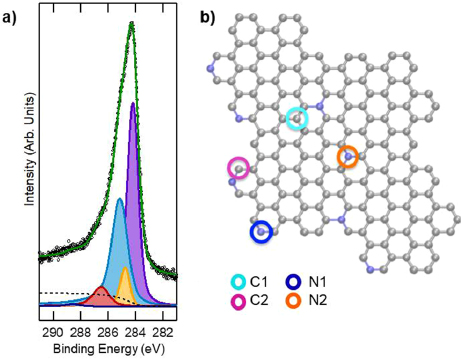
Figure IX.49. (a) C1s XPS spectrum of SLG/ Pt(1 1 1) after exposure to air and water. New components related with epoxy and hydroxyl groups appear as a tail of the main C-sp2 one. (b) Schematic representation of N and C configuration of heteroatoms on a graphene flake related with the XPS peaks assignments. C1 (light blue): sp2 C atoms; C2 (purple): C–N pyridine ring; N1 (dark blue): N atoms in the pyridine ring interacting with the metal substrate (Cu in this example); N2 (orange): substitutional N atoms in the graphene network. Adapted from [1577] with permission of the PCCP Owner Societies.
Download figure:
Standard image High-resolution imageTable IX.2. Binding energies of graphene C atoms in different chemical states. C1, C2, N1 and N2 are related with the scheme of figure IX.49(b) and represent C-sp2 (C1), C-N pyridine (C2), N atoms in the pyridine ring interacting with the metal (N1) and substitutional N atoms in the graphene network (N2). In addition, binding energies of C-metal, sp3 configuration, radical-N, epoxy and hydroxyl groups are also given. The values may slightly change depending on substrate.
| C1 | C2 | N1 | N2 | R–N–C | C-metal | sp3 | C–OH | C–O | C=O | O–C=C/C–C=O | |
|---|---|---|---|---|---|---|---|---|---|---|---|
| Binding energy (eV) | 284.4 | 285.9 | 398.0 | 400.6 | 399.5 | 283.2 | 284.7 | 285.4 | 286.7 | 288.5 | 290.5 |
| Ref | [1577] | [1577] | [1577] | [1577] | [1340] | [1577] | [1035] | [926] | [926] | [926] | [926] |
It is important not to mistake the contamination of graphene with GO. RGO can be derived from GO by reducing it with chemical reducing agents. This process can be followed by XPS by evaluating the ratio of the component ~286.5 eV (mainly C–O bonds) with the C-sp2 [1578].
Heteroatoms. In some cases one may be interested in the binding energy not of the C atoms, but of other elements covalently linked to graphene. The most important case corresponds to N heteroatoms. Its binding energy strongly depends on the adsorption configuration inside the graphene network. A scheme C and N atoms configuration in relation with the XPS components is shown in figure IX.49(b). Four possible configurations are shown: C-sp2 (C1, light blue circle), C in a pyridine ring (C2, purple circle), N in the pyridine ring interacting with the metal substrate (Cu for this case) (N1, dark blue circle) and a substitutional N in the graphene network (N2, orange circle). The XPS binding energies in these particular configurations are in table IX.2.
IX.2.3.1. Graphene grown on SiC
XPS characterization of C-rich SiC(0 0 0 1) surfaces can be used to extract the degree of graphitization. SiC surfaces prepared in UHV conditions present a series of surface reconstructions depending on the C/Si stoichiometry [1579]. For T > 1350 K, Si depletion from the surface eventually leads a reconstruction presenting a (6 √ 3 × 6 √ 3)R30° LEED pattern [592, 645, 659, 1580, 1581]. The atomic structure is normally described as a graphene-like honeycomb carbon layer highly buckled and partially covalently bonded to the uppermost Si layer [1582] (see section IV).
This covalent interaction alters the electronic properties of the graphene-like layer and it becomes a semiconductor [594]. XPS is presented in figure IX.50. The lower spectrum is an overview on a (6 √ 3 × 6 √ 3)R30° surface. The C1s peak (284.8 eV) has higher intensity than the two Si-related peaks: Si2p (101.4 eV) and Si2s (152.0 eV) [926, 1570]. The C1s/Si2p ratio is ~1.15 for 1486.6 eV, indicating that the surface is C-rich [659].
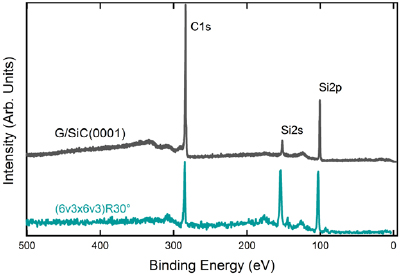
Figure IX.50. Lower spectrum: (6 √ 3 × 6 √ 3)R30° surface using an Al Kα anode (1486.6 eV) as x-ray source. Upper spectrum: synchrotron radiation XPS overview of SLG/SiC(0 0 0 1) annealed at 1400 K for 600 eV photons.
Download figure:
Standard image High-resolution imageA SLG/SiC(0 0 0 1) spectrum is presented in figure IX.50 for comparison. The upper black spectrum corresponds to a synchrotron radiation-based overview of a sample annealed at 1400 K recorded with a photon energy of 600 eV [1583] The C1s peak dominates, with C1s/Si2p ~ 2.53, which indicates a higher C concentration on the surface than in the (6 √ 3 × 6 √ 3)R30. The good resolution of the XPS in figure IX.51 allowed to decompose the peaks into their curve-components, which results from a convolution of a purely Lorentzian one (FWHM, 0.12–0.2 eV) with a Gaussian distribution (FWHM, 0.4–0.7 eV) [1584].
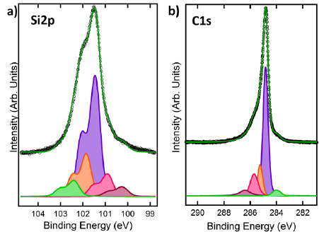
Figure IX.51. (a) XPS Spectrum of Si2p peak of SLG/SiC annealed at 1400 K recorded with a photon energy of 150 eV. (b) XPS spectrum of C1s peak of SLG/SiC annealed at 1400 K recorded at 400 eV.
Download figure:
Standard image High-resolution imageC chemistry is very rich and the interpretation of the C1s spectra is complicated. One could decompose the C1s peak of SLG/SiC(0 0 0 1) in five components. That at 284.83 eV can be assigned to C-sp2, and is the biggest contribution to the C1s core level peak, with 58.2% of the total area. This is used for calibration of the the Lorentzian and Gaussian widths. The components at lower binding energies (283.98 eV) can be attributed to carbides [1585], due to the C in the SiC bulk [588, 589]. There are three other components at higher binding energies, which can in principle be assigned to different configurations of C in the rearrangement that takes place on surface reconstruction [589]. These can be assigned to surface-related peaks: C-Si 1 at 285.26 eV (orange component in figure IX.51(a)), C–Si 2 at 285.73 eV (pink component in figure IX.51(a)) and S. C-Si 3 at 286.4 eV (bordeaux component in figure IX.51(b)).
The Si2p curve can be decomposed in five Si doublets. Based on H adsorption it is possible to distinguish surface-related from bulk-related components. Three components present intensity decrease upon H exposition. The intensity of the components at 100.4, 101.45 and 101.85 eV decrease ~15% after H exposure, while the other two at 100.9 and 102.4 eV present a small (3%–4%) increase [1585]. This suggests that the components which decrease and those that increase are related to surface and bulk Si atoms respectively.
IX.2.4. ARPES
ARPES is a technique that extracts the information retained by the electrons, emitted from a solid surface upon excitation with a photon. Due to the confinement of the electronic wavefunctions in the (x,y ) plane, the band structure of GRMs can be fully determined through angle-resolved photoemission spectroscopy (ARPES) [1586–1588]. This technique takes advantage of the photoelectric effect [1589], hence UV or soft x-ray radiation is used to extract electrons from the investigated sample.
The photons can be generated by laboratory sources, such as He or Hg lamps, or by synchrotron radiation. During photoemission, the crystal momentum of the electron inside the material is conserved in the plane parallel to the samples's surface. As a consequence, one can relate the electron's crystal momentum with the photoemission angle and determine the band structure. A typical experimental set-up for ARPES is sketched in figure IX.52. The radiation is shone over the sample so that the photon beam and the analyzer lay in the same plane. The photoemitted electrons are collected, within a certain angular acceptance, through a series of focusing electrostatic lenses into a hemispherical analyzer. Here, only the electrons with a certain kinetic energy E0 travel in the middle of the hemispherical capacitor. The width of the energy window about E0 is called pass energy, and it is a relevant parameter in determining the energy resolution of the instrument. The other important parameter is the radius of the hemispherical capacitor. Finally, the electrons impinge onto the detector, which in most cases is a fluorescent screen. A charge-coupled device (CCD) camera records the light intensity emitted by the detector.
Figure IX.52. ARPES set up scheme. Electromagnetic radiation provides enough energy for electrons to the sample to leave and travel towards the analyzer.
Download figure:
Standard image High-resolution imageIn the UV, soft x-ray regime, the momentum carried by the photon  is negligible compared to the crystal momentum of the electron
  , and this ensures the identity between the final and initial electron momentuma, i.e.
  . Hence, the von Laue equation
  is fulfilled, where
  is a base vector of the crystal's reciprocal space. Experiments are usually performed using photon energy <100 eV corresponding to a momentum
  . In the so-called sudden approximation, the electron is extracted instantaneously −from the material with no time to interact with the remaining N − 1 electrons [1586]. This allows one to consider the obtained dispersion as the non-interacting state of the system, or the one particle dispersion. As a consequence, for GRMs, the emitted photocurrent takes the form [1792]:

where  is the matrix element of the transition from the initial (i) to the final (f ) state,
  is the spectral function,
  is the Fermi–Dirac distribution and B is a background term coming from inelastically scattered electrons. The spectral function takes into account the angular dependence of the photoemitted electrons.
When the electrons leave the material, they end in a free particle state. Considering the scheme in figure IX.53 and assuming the conservation of the electron momentum parallel to the surface, the following expression holds [1586]:
where  is the emission angle and
  is the kinetic energy. When considering the perpendicular component, the description is not this simple, since it is not conserved when crossing the crystal surface [1586]. An expression to determine it is [1586]:
where V0 is the inner potential, defined as the energy difference between the vacuum level and the top of the valence band.

Figure IX.53. Momentum component conservation at the crystal vacuum interface. Only  is conserved.
Download figure:
Standard image High-resolution imageThe resolution on the measurement of  is:
is:
where  is the angular acceptance of the analyzer.
If the electron signal is spin-filtered, e.g. by letting it passing through a Mott detector, it is possible to reveal the contribution of a single spin component projected onto the detector's plane [1590] on a particular band. This technique is called spin-resolved ARPES (SARPES) and it is fundamental for determining the spin-polarization of electronic bands.
A recent development in ultra-fast lasers gave the opportunity to realize facilities for pump-probe experiments that can access the time scales of the quasiparticle dynamics in solid-state materials [1794]. Time-resolved ARPES (Tr-ARPES) is being used more and more to investigate the carrier dynamics in GRMs as well as charge transfer in LMhs.
IX.2.4.1. ARPES on graphene and vertical LMHs
A large amount of photoemission measurements have been carried out on graphene since the early 1970s [586, 663, 664], and ARPES measurements have since mapped the dispersion of the π-bands over the entire BZ.
The energy loss due to quasiparticle excitation, the electron phonon interaction in π and σ bands [671, 1591–1593] were investigated. Graphene on metals [1594], exfoliated, suspended and GNRs [592, 618, 620] have been measured. Perhaps the most investigated graphene with ARPES is that grown on SiC, because it has cm2 area coverage, and because of its flatness (figure VII.10) [592, 671, 673, 679, 1591].
The electronic properties of buffer, 1LG, 2LG, 3LG have been characterized by means of ARPES [598]. Quasi-free standing graphene on SiC has been investigated [645, 647, 678]. This method can be applied also to other LMs, such as TMDs [1595], and their combination in vertical LMHs [1217, 1596]. The possibility of studying the electronic properties of such a structure allows for understanding how the layers interact with each other.
The band structure of WS2/SLG can be retrieved by means of µ-ARPES on a single WS2 crystal. µ-ARPES (or micro-spot ARPES) is a technique capable of measuring the electronic properties of a material with a spatial resolution ~1 µm. The price for the higher spatial resolution is paid in terms of energy resolution, which is slightly worse. Figure IX.54(a) show a LEEM image of a single triangular WS2 crystal on graphene on SiC [1217].

Figure IX.54. Micrograph of a single WS2 crystal. Areas with different contrast are labeled MLG, BLG and WS2, respectively. Red arrows indicate the crystallographic orientation of WS2 crystal. Adapted from [1217] with permission of The Royal Society of Chemistry.
Download figure:
Standard image High-resolution imageOverlapping ARPES measurements with DFT minimizes the error in interpreting the measured signal. Figure IX.55(a) reports the graphene π- and π*-bands measured via µ-ARPES on the crystal shown in figure IX.54. The bands are well visible and highlighted by orange dots, corresponding to DFT bands on the graphene single cell. Calculated graphene σ-bands are not superimposed, since they are not detectable due to their low intensity. The bands visible in Γ belong to WS2, as also indicated by DFT. At the points where the bands of graphene and WS2 cross (indicated by green arrows in the panel), no apparent splitting or gap is observed. In order to confirm this, DFT calculations were carried out, the result of which is summarized in figure IX.55(b), where the bands 'unfolded' onto graphene's BZ are displayed for better readability.
Figure IX.55. Band structure of WS2/MLG. (a) µARPES measured on a single WS2 triangle with photons~70 eV. (b) DFT band structure evaluated on the WS2/graphene supercell depicted in panel (c) and unfolded into graphene's BZ. (c) Coincidence supercell (7 × 7) over (9 × 9) of WS2/graphene. (d) Experimental ARPES CESs recorded with p-polarized photons ~ 27.5 eV (e) Experimental ARPES band structure of WS2/EG measured with He I light along the path indicated in the inset by the red line. DFT bands including spin–orbit effects are overlapped to the raw data. On the right: zoom-in of the region around  (green-dashed line in panel (e)). Both DFT and experimental bands fit are superimposed to the raw data. The red-dashed line is on the graphene's π-bands. Adapted from [1217] with permission of The Royal Society of Chemistry.
Download figure:
Standard image High-resolution imageWhen crystals with different lattice parameter are superimposed, they can give rise to a superlattice. When multiples of the different unit cells match in size, they form a supercell which behaves as a new unit cell of a hybrid crystal. This new periodicity alters the overall band structure, opening minigaps in high symmetry points. The smallest coincidence lattice for the WS2/graphene system was found to be the (7 × 7) WS2 unit cells (u.c.) on (9 × 9) of graphene, figure IX.55(c). DFT calculations were carried out on this supercell and as a result, no mini-gap opening was predicted, unlike what observed for MoS2 on graphene [1596]. To better visualize the relation between the graphene π-bands and the WS2 bands, constant energy surfaces (CESs) are shown in figure IX.55(d), extracted from the Fermi surface (FS) at binding energies indicated in the figure. The CESs in this case are small volumes in k-space integrated over #250 meV, corresponding to the resolution of the instrument. The data were acquired with photon energy 27.5 eV in order to maximize the intensity of the WS2 bands with respect to graphene.
ARPES measurements with He I radiation of 21.2 eV are presented in figure IX.55(e), together with the DFT-calculated bands including spin–orbit coupling. The image was obtained by scanning the BZ along the red line traced within the green hexagon in the inset. In this image the high symmetry points are for the WS2 BZ, whereas for panels (a) and (b) they refer to graphene's BZ. Single spectra were measured perpendicular to the red line. The experimental data are fitted in the proximity (±~0.1 Å−1) of  with a parabolic function in order to extract the effective mass values of the holes. The result along the
  direction is displayed on the right side of figure IX.55(e), representing the zoom-in of the region framed with a green-dashed line in the panel. This gives mh1 ~ 0.39me for the low energy band and mh2 ~ 0.53me for the high energy band, confirming the asymmetry reported in Ref. [1597]. The spin–orbit splitting of the WS2 bands in K was retrieved from integrated energy distribution curves to be 462 ± 5 meV. This is ~10% larger than what was measured for 1L-WS2 on Au(1 1 1) and Ag(1 1 1) [1598, 1599] and ~7% larger than the highest value reported so far [1599]. This is comparable with measurements on bulk WS2 [1594].
IX.3. Electrical characterization
IX.3.1. Four probe configuration
The basic electronic properties of a homogeneous metallic diffusive material are captured in the primary parameters: resistivity ρ (Ω · cm), n (cm−3) and µ (cm2 V−1 s−1). For a LM, the resistivity is replaced by RS (Ω), i.e the resistance that would have a (homogeneous) sheet of material with equal length and width. For a sheet of thickness t, RS = ρ/t. Similarly the surface charge density ns (cm−2) is ns = n t where σ is the conductivity. σ/(ne) = 1/(nseRS). It is usual to define µ = σ/(nse) = 1/(nseRS). It is common in the GRM literature for RS to be written as ρxx.
Resistances are measured in a four-probe configuration, where a current I is applied on 2 probes (source and drain) and the voltage drop V measured on two others following the schemes in figure IX.56. This removes the contribution from contacts, i.e. that of the leads (wires), to the measurement apparatus, so that the measured resistance V/I is intrinsic to the sample. In a linear configuration (figure IX.56(a) and Hall bar figure IX.56(b), RS = (VCD/IAB)·(W/L), where W and L are the width of the sheet and distance between the voltage probes C and D, respectively. In a Van der Paw configuration [1600] (figure IX.56(c)), contacts are attached to the edges of a sheet and RS = π(RAB,CD + RBC,DA)/[2Ln(2)]. f (RAB,CD/RBC,DA), where RAB,CD is the resistance measured injecting the current between A and B and the voltage probes are C and D. RBC,DA is measured by permutation. The f is a function of RAB,CD/RBC,DA only, and satisfies the condition [1600]:
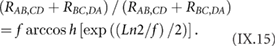
f is plotted in figure IX.56(f). The Van der Pauw configuration allows measuring a sheet of arbitrary shape, like a cross e.g.
Figure IX.56. (a) 4-probe configuration. (b) Hall bar. (c) Van der Pauw. (d) TLM configuration; (e) FET, showing a SLG with a top gate deposited on a dielectric, and source and drain contacts. (f) f coefficient of the Van der Pauw method.
Download figure:
Standard image High-resolution imageStandard techniques [1601] are used to measure the SLG resistance. This is usually in the range a few tens Ω to a few 100 kΩ. In the low current range, low-frequency (typically a few Hz to a few kHz) AC measurements with a lock-in amplifier, either in current or voltage source mode, provide the best SNR. I-V characteristics are measured in DC mode, or by recording the current change (Iac) induced by modulating the voltage around a DC bias (V = Vdc + Vac). In all cases, the current must be kept low enough not to heat the sample, or to induce changes. At cryogenic T, typical currents range between nA to hundreds µA. High currents (~mA per µm width) can be used to anneal SLG to clean up impurities [1602, 1603] or to produce narrow constrictions tens of nm wide in suspended SLG [1604].
Ultra-high frequency measurements (>100 GHz [1605–1607]) or high precision resistance measurements for quantum Hall effect [612, 635] require specialized equipment.
The charge density is determined either from the Hall effect, or from electrostatic field effect. The Hall voltage, VH, is measured perpendicular to both current and magnetic field. Typically Hall bars such as in figure IX.56(b) are used. With the magnetic field B perpendicular to SLG and current from A to B, VH = VCE = VDF. For SLG, nS = B/(eρxy), where ρxy = (VH/I). In the van de Pauw geometry, current leads and voltage probed are placed in cross configuration, such that ρxy = VAC,BD = VBD,AC following figure IX.56(c).
In the simplest approximation, µ is deduced from resistance and charge density measurements: µ = ρxy/(Rsq B). In the simplest picture of short range scatters, the Boltzmann conductivity σ is independent of energy, i.e. independent of n [1608]. In this picture, the usual definition σ = nseµ, would give µ with unphysically large values at charge neutrality. In reality, σ varies with ns, being minimum at and around charge neutrality. This calls for other scattering mechanisms, like charge impurity scattering or resonant scattering [1608]. A better description of the relation between σ and n was given in Refs. [1608, 1599]:

as shown in figure IX.57. Here nimp is the charge impurity concentration, K/nimp has the unit of mobility and σres reflects the fact that SLG conducts even at zero carrier density [1610].
Figure IX.57. σ versus gate voltage at 20 K in UHV, for SLG and three different K doping concentrations. Lines are fits to equation (IX.16) and give µ, and the crossing of the lines defines the points of the residual conductivity and the gate voltage at minimum conductivity (σres, Vg,min) for each data set [1599].
Download figure:
Standard image High-resolution imageIn the previous examples ns is modulated with an electrostatic gate. In principle this is a parallel plate capacitor, with one plate being the gate and the other SLG. Either SLG is deposited on the dielectric or vice-versa. In the former case, the gate below SLG (bottom gate) often consists of conducting Si (the gate) covered with a dielectric (SiO2) onto which SLG is deposited. All devices fabricated on the substrate are subjected to the same field when a voltage VG is applied to the Si gate. Top gates are realized by depositing a dielectric (Al2O3, HfO, SiN, h-BN, etc) on SLG, e.g. by ALD or thermal evaporation. Sputtering is not recommended since it damages SLG [1611]. This is followed by coating with a metal (Au, Al). Top gates are usually patterned and can be addressed individually to switch one device at a time. The gate can also be brought close to SLG from the side in the same plane as SLG (side-gate). If the gate itself is also made of SLG, this allows patterning the SLG device and the gate all at once [730, 1612].
In the top/bottom gate configuration, the simplest assumption gives a charge variation Δns induced on SLG as:
where ε and td are the dielectric constant and thickness of the dielectric. In most FET configurations the SLG channel is provided with only 2-contacts (plus the gate, see figure IX.56(e)), therefore the contact resistance is included in the measurements, which results in underestimating µ. More precise methods have been developed [1613, 1614]. For sufficiently large bias voltage, the n may vary along the SLG channel, an even change sign, due to the SLG ambipolar nature, leading to a complex interplay between VSDand VG (top, bottom or both) [1615]. Equation (IX.12) does not take into account the variation of chemical potential with n, which introduces an extra capacitance term e2D(EF) [1616], the so-called quantum capacitance per unit area, with D(EF) the density of states, which cannot be neglected close to the Dirac point [1616].
ns can also be determined from magnetoresistance measurements in high (generally several Tesla) magnetic fields, and at low (cryogenic) T by analyzing the periodic oscillations of the magnetoresistance (Shubnikov–de Haas oscillations) as a function of 1/B [107, 622, 1617]. Examples are given in Figure IX.58 for SLG on SiO2 and MLG on 4H-SiC(0 0 0 − 1). The 1/B oscillation period is BF = (h/4πe) with
with  = nsπ. With increasing field, the oscillations develop into the quantum Hall effect, and the quantification of Hall resistivity also give access to n [107, 1617]. These measurement techniques can be useful in case of mixed (electron and hole) doping in the vicinity of the Dirac point [1618, 1619].
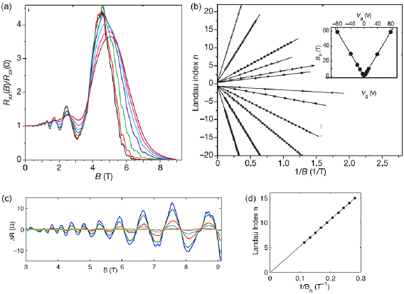
Figure IX.58. Shubnikov–de Haas oscillations of the magnetoresistance in (a) and (b) SLG on SiO2 [1617] and (c), (d) MLG on 4H-SiC(0 0 0 −1) (C-face)[1620] for different T from 4 to 70 K. (b) The minima in ρxx are plotted as a function of 1/B (so called fan plots) to determine the charge density at a particular gate voltage. (d) Same analysis for the data in (c), but plotting the maxima in ρxx.
Download figure:
Standard image High-resolution imageIn semiconductors a current saturation regime is reached by applying a sufficiently large VSD, and µ can be deduced from the current saturation value [1621]. However, this regime is difficult to reach in SLG because of the requirement of extremely high VSD, which will cause inhomogeneity in n along the channel [1615, 1622].
Standard electrical measurements require contacts on SLG. Besides the fundamental interest of how to inject from a 3d to a 2d material, from planar (2d) or edge (1d) contacts, while matching energy and momentum (at charge neutrality the SLG Fermi surface is reduced to points in k-space), it is technically difficult to realize contacts to SLG of low (in the 10 s Ω) resistance. Because there are no dangling bonds to adhere to, metals like Au tend to bead up on SLG [1623], which requires an adhesion layer, like Pd, Ti or Cr. Low resistance contacts (50–100 Ω µm) are a combination of mechanical adhesion and charge transfer to SLG, due to a large metal-SLG work function difference (to increase the SLG conductivity under the contact by heavily doping it) [1624–1626]. Metal induced doping can create p-n junctions from the SLG under the contact to the channel, which have to be taken into account in the resistance analysis [1625, 1626].
Contacts are usually defined by lift-off after development of the lithographic resist. Resists commonly used are positive e-beam resist (e.g. 200 nm PMMA spun onto 200 nm MMA), or photoresist (e.g. S1813 ~ 1.8 µm thick). Good contacts are obtained with 5–10 nm Cr, Pd, Ni or Ti (or combination of these metals, Ti/Pd 2 nm/10 nm) evaporated on SLG, followed by 30–50 nm Au, by e-beam or thermal evaporation. The contact resistance, Rc, can be measured by the transfer length method (TLM), see figure IX.56(d). A SLG strip is provided with a series of contacts. The 2-point resistance RTLM = Rc(W) + 2Rs L/W is measured and plotted as a function of distance L between the contacts, with W the channel width. The advantage is that this apporach fast and involves only resistance measurements. However this assumes that contacts the same, and Rs constant along the graphene channel (i.e, homogeneous scattering, homogeneous gate or bias induced charge density). This may be questionable very close to the contacts, due to metal-induced doping. Alternatively, Rc can be derived from Kelvin probe microscopy, by measuring locally with an AFM tip the voltage drop from contacts to channel [1627]. The lowest intrinsic Rc measured are in the range ρc = Rc · W = 50–100 Ω µm [1607]. Ref. [1628] developed edge contacts, where lateral contacts inject current through the SLG edges. RC are of the same order of magnitude [1628].
Deposition of gate dielectrics is a challenge for the same reason that metals do not adhere on SLG. ALD or evaporation of high K dielectrics (Al2O3, HfO2, SiO2) [1629] or Si3N4 [1630] have best RF performances (in terms of cut-off frequency) [585], [1631], and hBN encapsulation provides protection [1184, 1632].
SLG was the first measured LM that was exposed, i.e. not buried at the interface between two semiconductors. While this presents great opportunities (spectroscopy in particular), exposure to the ambient degrades the SLG pristine properties, by doping and scattering by impurities. The transport properties drift with a time constant ~1 h or so, and are recovered after annealing (e.g. ~1 h at 420 K in He) [1633]. SLG protection is therefore required (top layer, or measurement in neutral or vacuum environment), unless the exposure provides useful counter doping (like for the measurement of the quantum Hall effect [625]).
SLG is a flexible membrane, therefore the roughness of the substrate matters. Sharp ripples or bubbles introduce field gauge effects [450, 632], equivalent to high magnetic field of up to several hundred Tesla [632], with consequences on transport [450].
It is relevant for graphene nano/microstructures of size L × W to keep in mind that the energy scale is set by  , so that the energy separation between modes in charge neutral SLG is ~20 K for L = 1 µm. Therefore, submicrometer structures of SLG at low T are effectively quantum dots [620].
1d ballistic transport was measured in GRNs at RT [620]. In this case the nature of the contacts (invasive or not) determines the voltage. For invasive contacts the electron flow is interrupted by the voltage probe which then acts like a current injector, and a resistance close to the quantum of conductance Rq = (e2/h)−1 = 25.812 kΩ is measured independent of distance between voltage probes, even in a 4-probe configuration [620, 1634].
IX.3.2. THz-TDS mapping of electrical properties
Rs, µ and n can also be measured quickly, accurately and non-destructively using terahertz time-domain spectroscopy (THz-TDS)[1635–1639, 1641–1643]. This method has been thoroughly benchmarked against van der Pauw electrical measurements with fixed electrodes [1638, 1643] as well as scanning micro four-point probes [1636, 1637, 1795].
THz-TDS is based on the fact that the absorption in the THz range is highly dependent on the complex-valued and frequency-dependent electrical conductivity [1644]. This is because the absorption of light in the THz frequency range is dominated by low-energy intra-band transitions, as opposed to the inter-band transitions that give rise to graphene's constant absorption of light in the visible spectrum [1645].
The electrical field attenuation caused by the charge carriers in the thin film can be established by dividing the electrical field,  , through the sample area, with a reference,
  , from an area without the conducting film, which is then related to the conductivity through [1641]:
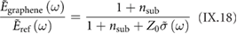
where  is the refractive index of the substrate,
  is the free-space impedance, and
  is the frequency-dependent (complex-valued) Drude conductivity,
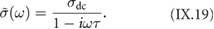
The THz radiation is focused into a 300 µm spot, limited by the long wavelength in the THz frequency range, which enables the average sheet conductivity (or resistivity) of a graphene film to be determined. In contrast, electrical measurements probe the device conductance (or resistance), which can differ significantly from the average conductivity for the same device area, in case of spatially non-uniform conductivity [1637, 1642].
Figure IX.59(a) is a conceptual schematic of a THz absorption setup, with a femtosecond laser pulse hitting a photoconductive antenna (PCA). The resulting THz pulse is focused by a lens, and transmitted through a thin conductive film. Finally, after refocusing by another lens, the attenuated THz pulse is picked up by a PCA operating as a detector. Figure IX.59(b) is a photo of a Si wafer covered with graphene, which is raster scanned across the focal plane of the beam line, while acquiring THz-spectra at a rate ~1 Hz. In figure IX.59(c) the time-resolved electrical field is shown. The initial peak is followed by smaller echo peaks, spaced by the round trip time of flight for internal reflections inside the substrate. Using equation (IX.18) the real (green triangles) and imaginary (green circles) parts of the conductivity can be plotted against frequency (figure IX.59(d)), and fitting the Drude conductivity (equation (IX.19)) yields the low frequency (DC) limit of the conductivity,  , and the momentum relaxation time (elastic scattering time),
  [1641]. Under the assumption of diffusive transport, the semiclassical Boltzmann transport equation,
  in combination with the fundamental relation
  yields expressions for n and µ that can be calculated from the fitting parameters
  :
:
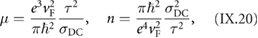
where e is the electron charge,  is the Fermi velocity, and
  is the reduced Planck constant. Therefore, the average µ and n can be spatially mapped with a resolution approximately equal to the THz spotsize
  , by recording a full spectrum in every pixel, and computing equation (IX.20) with the Drude fitting parameters.
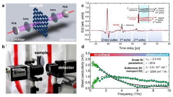
Figure IX.59. (a) Schematic of THz-TDS setup. (b) Photo of equivalent THz beam line, with a graphene-coated Si wafer held by a motorized raster scanner. (c) THz direct pulse and weaker echoes from multiple internal reflections. The black curve is from an uncoated reference area, while the red curve is attenuated by the conducting sample. (d) Conductivity spectrum of graphene grown on single crystal, which closely follows the Drude model (equation (IX.18)). The fitting parameters  can be used to calculate n and µ. For large-area conductivity mapping, commercial spectrometers that cover up to 2–3 THz are used, while a more sophisticated air-THz setup allows spectra up to 15–20 THz to be recorded [1637].
Download figure:
Standard image High-resolution imageFigures IX.60(a)–(c) shows the conductivity map of the same CVD grown graphene film before and after definition of 49 test devices, verifying that the laser ablation/shadow mask device fabrication method has little impact on the device characteristics, due to the complete absence of solvents and resists [1640, 1642]. Figures IX.60(d) and (e) show the µ and n maps obtained by the methodology described above, with the histograms below showing both the scale and distributions of values within a rectangular zone indicated with dark dashed lines. Figure IX.60(f) shows how the method can be used to map the large-scale changes in uniformity of electrical key parameters with growth T in a CVD process, indicating that higher T tends to give more uniform growth and larger usable areas of graphene [1641].
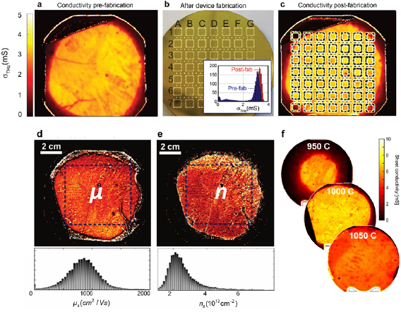
Figure IX.60. Examples of THz-TDS electrical characterization of graphene. Conductivity of graphene coated Si wafer mapped before (a) and after (c) fabrication of 49 electrical devices to test how individual process steps affect the conductivity [1641]. (b) wafer after laser-etching and physical mask deposition of metal contacts [1796]. Histogram (inset) of the sheet conductivity across the wafer before and after fabrication. (d) and (e) µ and n for a Si wafer determined by equations (IX.20), with histograms below showing scale and distribution of n and µ [1638]. (f) Investigation of how CVD growth T affect large-scale uniformity of sheet conductivity of graphene transferred to 4'' Si wafers [1641].
Download figure:
Standard image High-resolution imageThe THz mapping technique can be used for graphene on flexible substrates [1641, 1643]. Graphene grown on Cu, transferred to PET and doped by AuCl3 showed very high uniformity across 15 inch (25 × 30 cm2) PET sheets. The THz-resistivity in the frequency range (0.9–1.0 THz) is in figures IX.61(a) and (c), typically within 5%–10% of the DC Rs, as can also be seen by noting the small drop in  from 0 to 1.0 THz in figure IX.59(d).

Figure IX.61. (a) Terahertz resistivity maps (0.9–1.0 THz) of two A4 sized sheets of doped graphene on PET with (a) high and (c) lower uniformity (color scale is from 200 Ω to 500 Ω. The histograms corresponding to the white dashed rectangles are shown in (b), where sheet 1 shows a very narrow peak, while sheet 2 exhibits a bimodal distribution. (d) THz conductivity map of a  device, by THz and van der Pauw measurements. After Drude-fitting, the DC Rs is ~
 for the shown device, as for the histogram. The measurements for 7 such devices agree well, except device 4, which had a visible scratch. With permission from [1643], The Optical Society.
Download figure:
Standard image High-resolution imageThe histogram in figure IX.61(b) shows a very narrow distribution for sheet 1, and a broader, bimodal peak for sheet 2, consistent with the difference in the visual appearance of the THz resistivity maps (a and c). The histogram of DC Rs after fitting the Drude equation, equation (IX.19), to every pixel, shows a narrow distribution across the ~750 cm2 graphene area (dashed rectangle). Figure IX.61(d) is a THz map of a cm-sized device with the corresponding histogram of DC Rs. Rs by van der Pauw and THz mapping show excellent agreement, however, with larger statistical spread for the THz because of the avoidance of physical contact, and the greater number of measurement points. One of the devices (device 4) had a scratch, which typically offsets electrical measurements in unpredictable ways, while having little impact on the THz-measurements [1641].
THz-TDS electrical characterization can be done in transmission mode, the most used in literature [1641], or in reflection mode [1798]. Comparison of THz conductivity maps recorded in transmission (see figure IX.62(a)) and with a commercial reflection mode THz-system (DasNano, see figure IX.62(b)) showed negligible difference [1642], and good agreement with electrical measurements, for the same samples. Despite the large CVD graphene samples not being encapsulated, the measurements agreed well within the statistical errors, as clear from the conductivity histograms in figure IX.62(c) and the direct comparison between electrical four point probe sheet conductance with THz sheet conductivity measurements for both transmission and reflection mode systems in figure IX.62(d).
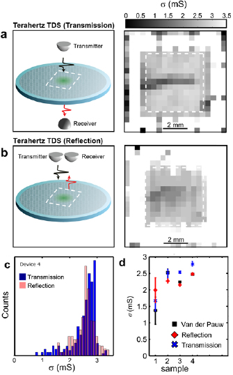
Figure IX.62. Comparison of (a) transmission and (b) reflection mode measurements on the same four samples, with comparable spatial conductivity pattern and (c) overlapping statistical distributions of measured conductivity (d) Direct comparison of van der Pauw four terminal measurements with reflection (diamonds) and transmission (crosses) measurements, showing good agreement except sample 1, which was less homogeneous compared to samples 2–4 [1642].
Download figure:
Standard image High-resolution imageFor transmission mode THz-TDS it is important that the substrate has high resistivity, to reduce THz absorption. The highly doped Si commonly used as a backgate, can be replaced by a custom-made substrate with a THz-transparent gate [1639] to enable THz-TDS and electrostatic gating on the same samples. The advantage of reflection mode is that there is no need for using high resistive substrates, while transmission mode can measure buried conductive layers at any depth.
THz-TDS is a fast, clean, and accurate way of measuring the transport characteristics of graphene on many substrates. Apart from Si and PET substrates, the method was used for graphene on SiC [1643, 1797] and graphene on Ge (on Si). As clear from figure IX.59(b) there is no limit for the size of samples, as a THz-TDS measurement head could easily be integrated in a roll-to-roll production line, giving instant feedback on the quality of graphene. The technique can also measure buried and encapsulated conducting layers, which provides essential information on the impact of intermediate process steps on the electrical characteristics before device fabrication.
IX.4. Mechanical characterization
GRMs compared to existing materials, combine high stiffness, strength, strain-to-failure and high flexibility [1646]. SLG compared to existing membranes has high ductility, as can be stretched up to 30%, however. Beyond that point it fractures in a brittle manner like glass [1647]. However, up to date, experimental evidence under uniaxial tension that confirms the above is missing, as these properties have been predicted via theoretical or modelling [1647, 1648]. The main reason for the lack of experimental data is associated with the sample quality (and size) and the damage inflicted by handling and subsequent transfer onto the loading devices. E.g. MC of graphite produces flakes of at best 100 × 100 µm2 depending on substrate interaction [1007]. Suspended SLG samples over relatively large areas (~ 1 mm2) as required for classical tensile experiments are difficult to produce [1007]. Wet methods for transferring CVD graphene from a metal substrate to arbitrary target substrates lead to samples with defects such as wrinkles, folds and tears, as well as residues, voids and polymer contaminants that can induce uncertainties in the measurements. Normally, optimization work has to be done in order to minimize the influence of defects and select the gauge area of the membrane to be tested. Due to limitations posed by the accuracy in force sensing in the nN range and sample gripping techniques, there is a lack of specialized instrumentation for in plane tensile testing of GRMs. This has triggered intense research for applying either AFM based, or thin film metrology techniques [1646, 1649]. A comparison of the measured mechanical properties with bulk materials is still an open question.
Measuring techniques can be categorized as direct and indirect. In direct methods the force or strain is applied directly to the GRM membrane. In indirect methods, Raman spectroscopy can be used for assessing the mechanical response of GRMs supported or embedded into polymers, where the strain is applied by shear forces from the deformed substrate. Other methodologies for applying strain are budge test and electrostatic actuation.
IX.4.1. AFM nanoindentation
The elastic properties of suspended SLG can be measured by nanoindentation using an AFM. The samples are made either by MC of graphite or by transferring CVD grown SLG onto pre-patterned substrates with holes or trenches. Usually an AFM tip applies a point load at the center of GRM sheets suspended over a hole on a pre-patterned substrate. Because of the high strength of SLG, higher than steel and Kevlar [1650], cantilevers with diamond tips are preferable for these experiments. For a doubly clamped SLG ribbon, a wedge indentation tip was used to introduce a uniform tensile strain [1651]. During nanoindentation the force, F, versus deformation, δ, of the suspended layer (at the point where the load is applied, figure IX.63(a) and (b)) is continuously recorded up to fracture. By employing third order elasticity theory and a number of assumptions based on classical membrane mechanics, the conversion of nanoindentation force-deflection measurements into an axial stress–strain curve for a free standing SLG membrane was performed (figure IX.63(c)) [1652]. By this procedure, the 2d Young's modulus, E2D, breaking stress,  , and strain at break,
  were estimated [1652]. In order to obtain the corresponding bulk parameters, these quantities were divided by the interlayer spacing in graphite h = 0.335 nm (assumed as SLG thickness) yielding values of Young's modulus ~1 TPa and of tensile strength of ~140 GPa [1652].

Figure IX.63. (a) Schematic of suspended SLG over hole for AFM nanoindentation. (b) SEM images of suspended SLG over holes. The border of the SLG-covered area is indicated by a dashed line. Wrinkles often present in the transferred SLG can be seen. (c) Force-displacement curve of SLG in AFM nanoindentation. The red line is a fit to equation (IX.22). Inset:AFM topography images of suspended SLG before and after fracture. Scale bars in (b) 2 µm and (c) 1 µm Adapted from [1653], with permission from AAAS.
Download figure:
Standard image High-resolution imageTo convert the experimental nanoindentation data to uniaxial stress–strain curves, GRMs are normally modelled as a membrane (thin plate) of negligible bending stiffness and nonlinear elastic properties [1652]. For doubly clamped beam shaped membranes (GNRs) [1649, 1651] the force-displacement behaviour can be expressed as [1649]:
For circular shaped membranes the corresponding relation is as follows [1652, 1653]:
In equations (IX.21) and (IX.22),  is the pre-tension in the membrane due to the preparation procedure, t is the thickness and ν is the Poisson's ratio (for SLG this is taken as 0.165, the Poisson's ratio for graphite in the basal plane [1652, 1654]). In equation (IX.21),
  ,
,  are the width and length of the GNR, while in equation (IX.22)
  is the hole radius and
  is a dimensionless constant [1649, 1654]. The microindentation experiment is in essence biaxial. The conversion of biaxial deflection data to uniaxial stress–strain curves by assuming zero bending stiffness is problematic, and not fully representative of true uniaxial tensile loading [1652].
AFM indentation experiments were conducted on graphene on SiC [1014] and CVD grown SLG of different grain size [1653]. Ref. [1653] showed that the elastic stiffness of CVD-SLG is similar to that of MC SLG, provided that the sample is free of pleats and ripples.
The mechanical properties of 1L-MoS2 [1655, 1656] and h-BN [1087] were measured by AFM nanoindentation. Similar modelling approaches were pursued for the interpretation of the force-displacement traces. In table IX.3 the elastic properties of various GRMs measured by AFM nanoindentation are summarized.
Table IX.3. Indicative values of Young's modulus and breaking strength for 1L-GRMs measured by AFM nanoidentation.
| 1L-GRM | E2D (N m−1) |  (N m−1) (N m−1) |
Strain-at-break (%) |
|---|---|---|---|
| Graphene (MC) [1652] | 340 (50) | 42 (4) | 25 |
| Graphene (CVD) | 328 (15) | 39.5 | — |
| MoS2 (MC) | 130 | 16.5 | — |
| MoS2 (CVD) [1657] | 123 | — | — |
| WS2 (CVD) [1657] | 137 | — | — |
| BN [1087] | 220–510 | 8.8 | — |
IX.4.2. Bulge testing
The elastic properties of GRMs can be assessed by bulge [1658] or pressurized blister test [1659], commonly applied for thin film testing. The advantage of the bulge test is the ability to measure not only E but also ν, whereas, in the case of AFM nanoidentation, ν should be known in advance (see equation (IX.22)) [1659]. Another advantage is that the stress concentration caused by the AFM tip is avoided by the application of a uniform pressure. In Ref. [1660] suspended MC SLG over microcavities (diameter ~ 5 µm) etched in a SiO2 substrate (figure IX.64(a)). The SLG membrane remains flat due to the balance of internal (atmospheric) and external pressures (figure IX.64(b)). It is adhered to the substrate by van der Waals forces and can confine gas molecules (e.g. N2). The SLG membrane inflates forming a blister, when a pressure difference across its surface is applied (figure IX.64(c)). AFM was used to define the SLG membrane shape and measure its maximum deflection  at the center of the blister and its radius
  (figure IX.64(d)). The deflection can be correlated with the pressure difference,
  , across the SLG membrane (figure IX.64(e)) using Hencky's solution [1661, 1662], which gives the deformation of the membrane for the geometrically nonlinear response of a clamped circular elastic membrane subjected to a pressure difference,
  , provided that the bending stiffness of the membrane is negligible. Therefore,
  can be written as [1660]:

where  is a constant that depends on ν.
Figure IX.64. (a) Optical images showing flakes with regions of 2–5 L (top) and 1 and 3 L (bottom). Schematic illustration of a SLG-sealed microcavity (b) at rest where Δp = 0, the pressure inside the microcavity is equal to the external pressure p ext, and (c) at higher Δp , (d) an AFM image showing the deformed shape of a SLG membrane with Δp = 1.25 MPa and (e) deflection versus position for various levels Δp (cyan). The dashed black line is the shape obtained from Hencky's solution for Δp = 0.41 MPa. The deflection is measured by an AFM along a line that passes through the centre of the membrane. Adapted from [1660], © Springer Nature.
Download figure:
Standard image High-resolution imageBy plotting  versus
  E can be estimated as the slope of the linear dependence. In figure IX.65(a) the experimental data for K(ν) δ3/α4 versus Δp are shown for SLG. A linear fit to equation (IX.23) gives E2D = 347 N m−1, in good agreement with the AFM nanoindentatation measurements [1008, 1653]. Ref. [1660] measured E of up to 5LG. The results are summarized in figure IX.65(b) and show that E2D is quantized to the SLG E2D (347 N m−1). These findings are based on a continuum model in which SLG is considered as a membrane with negligible bending stiffness and the crystal is of high structural quality i.e. free of ripples, folds and defects.
Figure IX.65. (a) K(y )δ3/α4 versus Δp for SLG membranes before delamination (black symbols) and after delamination (magenta), (b) nEt versus number of layers n. Closed shapes are for the fitted lines; open shapes are for nEt, with Et = E2D = 347 N m−1.
Download figure:
Standard image High-resolution imageBulge testing has also been used for 1L and ML-MoS2 as a way to apply biaxial strains up to 7% for band gap engineering [1663]. The strong adhesion, comparable to solid–liquid adhesion [1660], between 1L-GRMs and an atomically flat substrate (e.g. SLG/SLG, SLG/hBN, MoS2/MoS2) results in atomically clean interfaces since any contaminants (water and hydrocarbons) are repelled by the van der Waals forces between the layers forming microbubbles [1664]. These bubbles have constant volume, and their shape is determined by the competition between van der Waals adhesion of the crystal to the substrate and the elastic energy needed to deform it [1665]. In figure IX.66(a), typical force-displacement curves (solid lines) recorded from bubbles of different sizes are presented. The symbols correspond to numerical fits by taking into account the changes in area of contact and the increase in bubble's radius [1665]. The data in figure IX.66(b) correspond to SLG bubbles for which the fitting curve to the experimental data is drawn by assuming a SLG axial stiffness ~420 ± 20 N m−1 [1665]. Similarly, the stiffness of 1L-MoS2 was estimated as 210 ± 20 N m−1. Both values are somewhat higher than those given in table IX.3.

Figure IX.66. (a) Experimental force-deflection curves (solid lines) and numerical fits (symbols) for two SLG and 1L-MoS2 bubbles of different sizes. (b) A force-deflection curve (solid curve) and corresponding numerical fits for three values of Y = E2D.
Download figure:
Standard image High-resolution imageIX.4.3. Fracture toughness and bending stiffness
Large-scale applications of GRMs, beyond microscale, require the knowledge of fracture toughness, rather than the intrinsic strength, which corresponds to a uniform breaking of atomic bonds in a perfect GRM crystal. Fracture toughness is a property that describes the ability of a material containing a crack or a defect to resist fracture [1666]. The absence of reliable tensile testing devices with force sensing at the pN or nN range and the cumbersome fabrication/transferring procedure has hindered progress. Thus, the direct determination of fracture toughness has been challenging for GRMs. Fracture data for CVD SLG were measured using in situ MEMS-based uniaxial tension devices in a Scanning [1667], Transmission [1428] electron microscope and AFM nanoindentation [1668, 1669]. Ref. [1667] conducted in situ tensile testing of centre-cracked CVD SLG in a SEM and obtained fracture toughness based on the classical Griffith's fracture theory [1670]. Ref. [1667] conducted in situ fracture toughness testing in a HRTEM on MLG having V/U-shaped single-edge notches. For comparative purposes fracture toughness testing on ML-h BN samples was also conducted. Ref. [1671] performed fracture mechanics experiments under uniaxial tension on MC BLG and measured its fracture toughness. In table IX.4 the measured fracture toughness for various SLG and MLG and ML-hBN are summarized.
Table IX.4. Fracture toughness of 1LG, 2LG, MLG ML-hBN.
| Sample | Fracture toughness MPa  |
Mechanical testing/device |
|---|---|---|
| CVD SLG [1667] | 4.00 | Tensile/MEMS device (SEM) |
| BLG [1671] | 21.25 | Tensile/MEMS device (SEM) |
| MLG [1428] | 12.00 | Tensile/MEMS device (TEM) |
| ML-hBN [1428] | 5.50 | Tensile/MEMS device (TEM) |
GRMs are modelled as membrane-like materials i.e. with approximately zero bending stiffness [1672]. Therefore, the effect of bending modulus is usually ignored [1652, 1653]. Refs. [1649, 1655] explored the effect of bending modulus as being proportional to the third power of the crystal thickness (see first term in equation (IX.21)) in AFM nanoindentation of MoS2 crystals with various thicknesses. The force-displacement curves for the FL crystals were strongly nonlinear, while for number of layers N > 10 were linear. This is important when considering membrane-to-plate like transition for N > 10. The determination of bending stiffness of either 1L or FL-GRMs has been mainly based on various types of theoretical calculation [1673]. Ab initio or first-principles quantum mechanical calculations and empirical potential calculations were used to determine the bending modulus of SLG [1646, 1673], with higher values (mean value ~ 1.51 eV) in comparison with those derived by empirical potentials (mean value ~ 1.12 eV). These models treat SLG as an isotropic body. To introduce anisotropy and to incorporate bending effects, a finite elasticity model was proposed [1674]. This provides the means to introduce (and handle) additional degrees of freedom through dependence on the shift vector which separates the two Bravais sublattices of SLG [1674]. Continuum mechanics was applied to describe the SLG flexural deformation, leading to a nonlinear von-Karman plate theory with two elastic bending moduli [1646, 1674, 1675]. However, from the experimental point of view, Ref. [1676] criticized the use of the continuum mechanics shell model. By exploring the nm scale rippling of SLG, Ref. [1676] claimed that phenomenology fails to predict correctly E2D, as well as the SLG thickness of 0.335 nm, since classical continuum plate theory assumes that bending always induces in-plane stretching.
A few attempts have been made to measure experimentally the bending stiffness of FLG and MoS2 and confirmed the dependence on the third power of thickness in accordance with the membrane theory of shells with pure bending [1673]. Ref. [1677] performed AFM nanoindentation in FLG membranes onto a circular hole, while Ref. [1678], fabricated and measured the bending stiffness of convex-buckled suspended BLG ribbons. By exploiting the abrupt switching from convex to concave geometry of the ribbons, under electrostatic actuation, they measured a bending rigidity ~35.5 eV. Ref. [1679] proposed a different experimental approach to measure the bending stiffness of 1L-GRMs. The method is based on atomic mapping of the crystal lattice within a fold by using HRTEM for SLG and scanning TEM imaging for MoS2 and WSe2. They confirmed the applicability of the linear elastic shell model and derived the bending rigidity. They found that bending rigidity for TMDs is in the range ~10–16 eV, five to six times that of SLG, in agreement with theory [1679].
Ref. [1680] measured the bending modulus of CVD SLG. They produced cantilever structures (length, 10–100 µm and width, 10 µm) and measured their spring constants by assuming them to be related to the bending rigidity. By using the photon pressure from an infrared laser, the spring constant of the cantilever and the bending rigidity was measured (figure IX.67(a)). Using the thermal fluctuations of the SLG cantilevers and based on the equipartition theorem of classical statistical mechanics, the cantilever spring constant was also measured independently (figure IX.66(b)). As shown in figure IX.67(c) both methods yield a high bending stiffness for SLG, ~103 to 104 eV. These values are orders of magnitude higher than 1.2 eV, predicted from simulations [1673] and measurements of the phonon modes in graphite [1681]. This high value is attributed to both thermal and static rippling stiffening ultrathin crystalline membranes in a manner similar to how a flat sheet of paper becomes more rigid when crumpled [1680].
Figure IX.67. Bending stiffness of SLG by (a) applying controlled forces using an IR laser and (b) tracking the motion of a rotated device under thermal fluctuations. (c) Stacked histogram of bending stiffness measured by the methods in (a) and (b). The red arrow points to the bending stiffness ~1.2 eV calculated theoretically. Scale bars are 10 mm. Adapted from [1680], © Springer Nature.
Download figure:
Standard image High-resolution imageIX.4.4. Raman spectroscopy
Information on GRM mechanical properties may be obtained by Raman spectroscopy combined with various types of external loadings (uniaxial, biaxial, hydrostatic, etc) [1529, 1682–1685]. Due to the anharmonicity of the interatomic potentials phonon frequencies soften upon tension and harden under compression [1529]. As a result, Raman peak positions red (blue) shifted under tensile (compressive) loading. The magnitude of shift depends on the interatomic force constants and the mode eigenvectors relative to the directions of the strain axis [1529]. However, in GRM many other effects can shift peaks, e.g. doping [1518], hence caution needs to be taken when using Raman spectroscopy to derive these information.
Several groups investigated the effect of uniaxial strain in tension or compression by bending flexible substrates (e.g. PDMS) or plastic beams (e.g. PMMA) on which GRMs are deposited without slippage [1529, 1536, 1546, 1686–1693, 1723]. The samples can be supported or embedded within a thin polymer film. In these experiments the application of uniaxial stress/strain leads to the development of interfacial shear between the GRM membrane and the underlying or surrounding polymer, transmitted into a normal stress [1694]. Care should be taken for the examined area of the flake to be free of residual stresses [1694]. Pos(G) is an indicator that the applied strain is transferred to the interatomic bonds, provided one can ensure that other effects, also leading to peak shifts, are not present. Under uniaxial strain the doubly degenerate E2g optical mode splits in two components, one polarized along the strain and the other perpendicular to it. This leads to the splitting of the G peak into two bands, which are usually called G+ and G− [1529]. Both peaks red shift with increasing tensile strain, and their splitting increases, in agreement with first-principles calculations. Their relative intensities are found to depend on light polarization, which provides a useful tool to probe the graphene crystallographic orientation with respect to the strain. A detailed explanation of these effects is also given in section IX.2/Raman and figure IX.41.
In tension, the shift of the main Raman modes is linear up to 1.5% [1695]. The 2D peak position downshifts with uniaxial strain at a much higher rate of ~ − 60 cm−1/% [1529, 1688]. An analogous but not as pronounced splitting to two distinct components 2D− and 2D+ was observed [1534, 1536] depending on laser wavelength. The strain-induced splitting and the red shift depend on the strain axis direction relative to the crystallographic axis. The underlying mechanism of the strain variation of the 2D peak depends on the shifting of the Dirac cones and the anisotropic phonon softening which, in turn, cause alteration in the scatterings paths participating in the double resonance mechanism for the 2D band [1534, 1696–1697].
Under compression, by monitoring the Pos(2D) shift of rectangular SLG embedded into polymer flakes of various sizes the critical strain-to-failure was determined [1692]. These were found to be independent of flake size at a mean value ~ −0.60% corresponding to a yield stress up to ~ −6 GPa [1691]. CVD SLG can be considerably wrinkled [1698]. Upon uniaxial deformation the Raman response for the 2D peak was <25% of that of flat exfoliated flakes [1698]. In all cases in which SLG is either supported on or embedded in a polymer matrix, parameters such as interfacial shear strength, onset of interfacial sliding and critical compressive strain-to-failure may be extracted via in situ Raman spectroscopy under tensile or compressive loading [1699, 1700].
Raman spectroscopy was also used to investigate SLG bubbles as a function of strain [1531, 1658, 1701]. These are formed by the pressure difference on both sides of SLG during the deposition of flakes over apertures of various size and shape. SLG membranes can support pressures up to 14 bar, corresponding to reversible strains up to 2% [1701]. The advantage of intentionally pressurized membranes is to avoid the influence of the substrate, excluding complications from SLG-substrate interactions. Biaxial strain enables the determination of the Grüneisen parameters. Ref. [1702] determined the SLG E2D by comparing the strain induced on pressurized balloons and the response of the G peak, with numerical simulations. The estimated E2D as 2.4 and 2.0 TPa, is much larger than previous values [1652, 1660]. This discrepancy was attributed to the small attainable strain (~0.2%), since E may depend on the strain range being larger in small strain ranges.
In Ref. [1689] an effective bending stiffness of SLG embedded into a polymer cantilever was estimated. Flakes of various aspect ratios (length to width) were embedded on the surface of a PMMA bar covered by a 200 nm PMMA layer. SLG was modelled as a thin plate and subjected to uniaxial compression [1689]. SLG was buckled at a critical strain determined by the response of the 2D peak (figure IX.68). Pos(2D) relaxed after an abrupt uptake, while the strain at the onset of the Pos(2D) relaxation defines the critical strain for each flake, see figure IX.68. For flakes with lengths smaller than the critical length (twice the distance it needs for strain to increase to the externally applied value) the externally applied strain is not fully transmitted to the flake [1687, 1694, 1698]. For flake lengths higher than the critical length, the critical strain for buckling is ~ − 0.6% [1692]. By considering the critical buckling strain for an embedded flake in the classical Euler regime [1672, 1689], the effective bending rigidity of SLG fully embedded in a polymer matrix was estimated ~70 MeV. This means that SLG encapsulation into a matrix affects the resistance to bending and paves the way for the development of novel composite materials with higher values of compression strength compared to conventional ones. This value, however, is six orders of magnitude higher than in air and one order of magnitude higher than CVD SLG in water [1680]. This could imply that encapsulation into a matrix or in water, affects the resistance of SLG to bending.

Figure IX.68. Pos(2D) as a function of uniaxial compressive strain for SLG flakes of various aspect ratios. Adapted from [1703] © Springer Nature.
Download figure:
Standard image High-resolution imageThe bulging test combined with Raman spectroscopy was used [1704] on a multireflection model for a SLG-air-Si stack (figure IX.69(a)) that takes into account the variation of I(2D) and I(G) (figure IX.69(b)). Both oscillate between a minimum and a maximum which depend on the height of the blister at various pressure differences (figure IX.69(c)) [1704]. The enhancement factor of I(D) and I(G) was correlated by a multireflection model [1705] with htot, the total distance between SLG and the underlying Si (figure IX.69(a) and (c)), and was used for the metrology of the blister height. Following Hencky's model (equation (IX.23)), the third power of the height at the centre point of the blister is linearly dependent on the pressure difference across SLG (figure IX.69(d)) resulting in a slope from which the suspended SLG E2D was estimated ~352 Nm−1, in agreement with values derived from direct methods (see table IX.3).
Figure IX.69. (a) Schematic of blister geometry. The optical path of the Raman signal and excitation is also depicted. SLG suspended over the hole (Inset), (b) enhancement factor for G and 2D. (c) I(G) and I(2D) versus distance from the centre of the hole with SLG at rest (0 kPa) and at a higher pressure difference. (d) Third power of SLG blister at its center versus pressure difference. From the slope of the linear fit, E is determined.
Download figure:
Standard image High-resolution imageInstead of using the pressure difference, the bulging test can be also implemented with electrostatic actuation of SLG suspended onto holes with large diameters (7.5–30 µm) over a gating chip forming a parallel plate capacitor with an inter-plate distance, d, (figure IX.70(a)) [1706]. By applying a gate voltage, SLG deflects subjecting to a pressure which defines the radial in plane stress and corresponds to a radial strain. Therefore E2D can be estimated (figure IX.70(d)). The radial strain depends on the height of the membrane dome at the centre deflection point, measured by employing interferometric profilometry (figure IX.70(b). A number of different devices were tested and the estimated E are presented in the histogram of figure IX.70(d) and are significantly lower than those from other techniques (table IX.3).
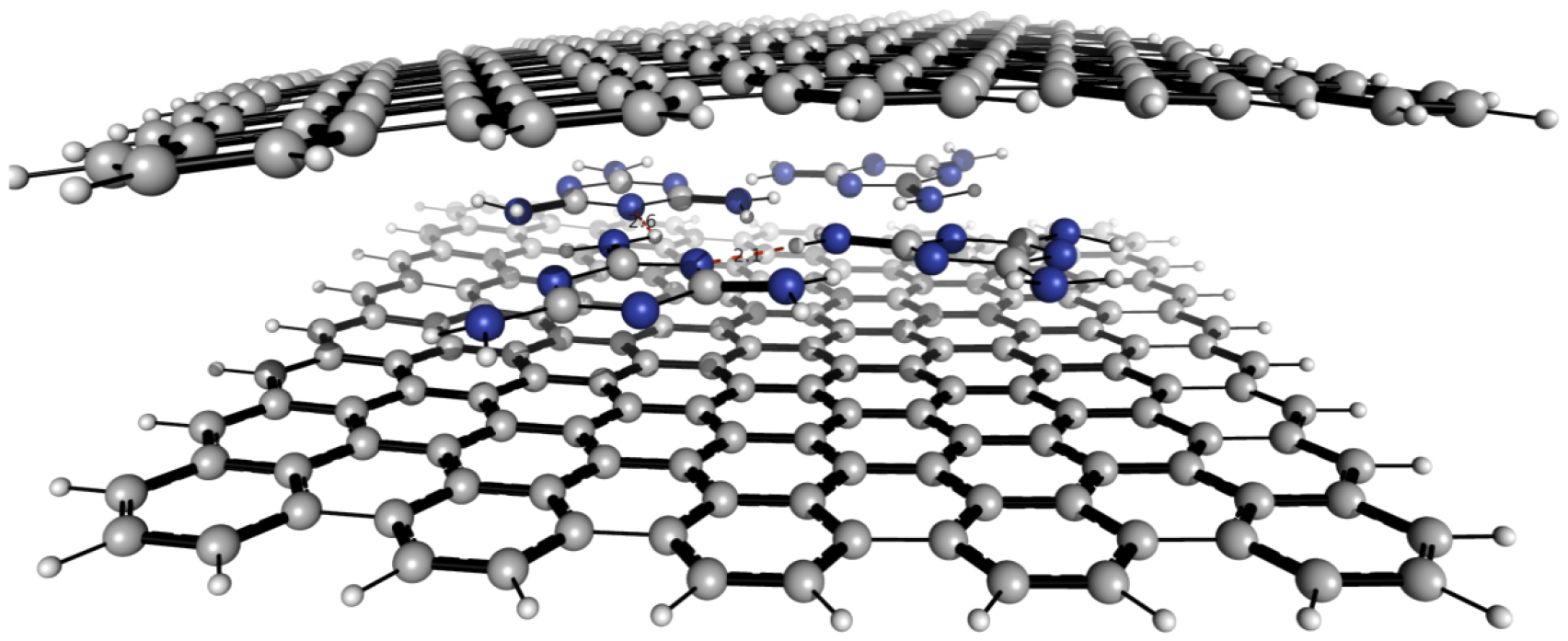
Figure IX.70. (a) Device schematic. Inset: SEM image of a representative free-standing SLG membrane (scale bar, 8 µm). (b) Cross-sections of SLG membrane at various applied voltages. Height data obtained from interferometric profilometry corresponding to these cross-sections are in the inset. Also shown is a 3d view of the data at Vg = 400 V. (c) AFM measurements of SLG membrane with nm-scale static wrinkles (left, scale bar, 100 nm). A cross section of the AFM data is shown in the bottom panel. Wrinkling is also evident on the high-angle tilted SEM image (right, scale bar, 1 µm). (d) Histogram for all measured CVD SLG devices.
Download figure:
Standard image High-resolution image
Ref. [1707] employed Raman spectroscopy using the aforementioned SLG-sealed micro-chambers under variable external pressure to determine the pressure induced sliding friction between SiO2 and 1L-, 2L- and 3LG. Tensile radial strain ~ 0.6% and compressive tangential strain ~ −0.3% were achieved. A violation of the Amonton's law [1708, 1709] for 1L and 2LG was found. In 3LG, however, the sliding friction is directly proportional to the applied load in accordance with the Amonton's law. This behaviour was attributed the lower bending rigidity of 3LG, enabling higher surface conformation and stronger adhesion.
Several diamond anvil cell experiments were conducted on MC 1L and FLG on Si/SiO2 or Cu, employing different pressure transmitting media [1529, 1710]. The choice of transmitting medium, e.g. polar (4:1 methanol-ethanol) or non-polar (e.g Fluorinert), is important due to pressure mediated doping that occurs from the substrate. Assuming that SLG follows the pressure-induced substrate contraction, its compression is determined by the bulk modulus of the substrate (140 GPa for Cu [1710]). In Ref. [1710] suggested that the expected value of the pressure dependent wavenumber shift is ~15 cm−1/GPa (for SiO2/Si, which is more compressible, this is ~21.4 cm−1/GPa). The significant deviation was ascribed to the non-ideal adherence of SLG on Cu.
From the applications point of view, it is important to understand how atomically thin membranes respond to mechanical deformations at the nanoscale. Sample preparation and handling hinders systematic studies, since a defect-free gauge area of the sample is difficult to be placed and gripped onto the loading device. The development of specific instruments with low force sensing and capable of applying in-plane stress in GRM membranes is necessary to capture their full response under axial deformation up to failure and to measure directly the elastic (e.g. stiffness) and inelastic properties (e.g. fracture strength and strain-to-failure). Fundamental questions have been raised on the effects of defects, out-of-plane deformations and wrinkling in either elastic or inelastic properties of GRMs [1669, 1711].Therefore, further research is needed in order for novel applications to take full advantage of these superior properties.
Conclusions
We presented the main techniques for production, transfer and functionalization of graphene, related layered materials, and heterostructures. We also summarized the key characterization techniques. We provided key practical details and procedures, to help the reader reproduce the results. We hope this work will stimulate both fundamental and practical interest in GRMs, and facilitate their use in a variety of novel applications. Acknowledgment
We acknowledge funding from the European Commission Graphene Flagship Core1 (grant agreement 696656) and Core2 (grant agreement 785219). We thank Dr Elena López-Elvira for editing this manuscript.