
Abstract
With first principles calculations, we predict a novel stable 2D layered structure for group VI elements Se and Te that we call square selenene and square tellurene, respectively. They have chair-like buckled structures similar to other layered materials such as silicene and germanene but with a square unit cell rather than a hexagonal one. This special structure gives rise to anisotropic band dispersions near the Fermi level that can be described by a generalized semi-Dirac Hamiltonian. We show that the considerably large band gap (∼0.1 eV) opened by spin-orbit coupling makes square selenene and tellurene topological insulators, hosting non-trivial edge states. Therefore, square selenene and tellurene are promising materials for novel electronic and spintronic applications. Finally, we show that this new type of 2D elemental materials can potentially be grown on proper substrates, such as a Au(1 0 0) surface.
Export citation and abstract BibTeX RIS
The isolation of graphene in 2004 [1] opened up a new avenue in condensed matter physics: two-dimensional (2D) materials research. Following the success of graphene [2], intensive efforts have been devoted to exploring other 2D materials [3]. Among them, elemental 2D materials (composed of only one element) have attracted much attention because of their simple composition and intriguing electronic properties [4]. A number of elemental 2D materials beyond graphene have been predicted and synthesized, such as silicene [5–8], germanene [9], stanene [10, 11], phosphorene [12], and borophene [13, 14], with elements ranging from group III to group V. However, few studies on group VI elemental 2D materials have been reported, although there are increasing interests in studying thin film Tellurium recently [15–18]. Unlike the aforementioned elements, at ambient conditions, most of the group VI elements have 3D bulk structures composed of 1D atomic chains or 0D atomic rings with only two-fold coordination bonding. The question remains whether these elements can also form 2D atomic layers as elements from groups III–V do.
During the exploration of 2D materials, some are predicted to be topological insulators (TIs), a new quantum state of matter recently discovered [19–23]. TIs have different band topology from normal band insulators and the former are characterized by a non-zero topological invariant called  invariant. The special band topology gives rise to gapless surface/edge states at the interface between TIs and normal insulators or vacuum. TIs are typically realized in systems with spin-orbit coupling (SOC). The momentum-dependent SOC has different effects on different spins, leading to the spin-momentum locking characteristic (helicity) of the surface/edge states. In the 2D scenario, when Sz is conserved (e.g. without Rashba-like SOC), spin up and down are correlated with opposite momentums, strictly prohibiting elastic back-scattering by non-magnetic perturbations as spin and momentum cannot be flipped simultaneously. Therefore, these gapless edge states form 1D conducting channels without dissipation. The helical edge states are also responsible for the quantum spin Hall effect (QSHE) in 2D TIs [19–21], in which the spin-Hall conductance is finite while the charge-Hall conductance vanished. Even when Sz is not conserved, the gapless edge states are still robust as they are protected by time-reversal symmetry [19]. These special properties make 2D TIs extremely appealing in novel electronic and spintronic applications.
In this study, we report the theoretical prediction of a new type of 2D layered structures for group VI elements Se and Te, which we call square selenene and square tellurene, respectively, following the symmetry of the unit cell and the naming convention of graphene. We confirm their thermal stability with ab initio phonon calculations and molecular dynamics (MD) simulations based on density functional theory (DFT). We found that pristine square selenene and tellurene display highly anisotropic cone-shaped dispersions near the Fermi level that can be well described by a generalized semi-Dirac Hamiltonian [24, 25]. Interestingly, the non-vanishing momentum-dependent on-site energy term in the Hamiltonian can give rise to negative effective mass for the low-energy carriers in the conduction band. Moreover, we show that square selenene and tellurene are 2D TIs with a relatively large bulk band gap (∼0.1 eV), enabling QSHE to be observed at room temperature. Finally, we show that this new type of 2D elemental materials can potentially be grown on proper substrates.
Using DFT calculations within generalized gradient approximation (GGA)7, we extensively investigate the lowest energy configurations for Se and Te in 2D. The main results are summarized in figure 1 and table 1. As in the case of 3D, Se atoms prefer to form two-fold coordination bondings in 2D. Therefore, the lowest energy structures for Se in 2D consist of 0D atomic rings or 1D helical atomic chains, as shown in figures 1(a) and (b), respectively. The Se–Se distances are around 2.4 Å within the rings or chains and larger than 3.1 Å between atoms in adjacent chains or rings. Thus, the interaction between adjacent atomic chains and rings are dominated by van der Waals interactions. These van der Waals structures in 2D can be grown on substrates, as observed in experiments when Se is deposited on metal surfaces [26]. However, they are easy to break upon isolation, and the electrons are mainly localized in 1D or 0D with minimum hopping between those 1D or 0D structures, limiting their applications in 2D devices.

Figure 1. Lowest energy structures for freestanding Se and Te in 2D: (a) Se rings, (b) Se chains, (c) square selenene, (d) rectangular tellurene, (e) square tellurene. The side and the top views of each structure are shown in the upper and lower panels, respectively. Se and Te atoms at different heights are highlighted with different colors. The unit cell is indicated by black solid lines. The values of the structural parameters a1, a2, and d are given in table 1.
Download figure:
Standard image High-resolution imageTable 1. Calculated cohesive energy Ec and structural parameters (a1, a2 and d) for the lowest energy freestanding structures of Se and Te in 2D shown in figure 1.
| Structure | Ec (eV) | a1 (Å) | a2 (Å) | d (Å) |
|---|---|---|---|---|
| (a) Se rings |  |
8.80 | — | 1.74 |
| (b) Se chains |  |
4.01 | 4.98 | 1.76 |
| (c) Square selenene |  |
3.65 | — | 0.77 |
| (d) Rectangular tellurene |  |
4.17 | 5.49 | 2.16 |
| (e) Square tellurene |  |
4.08 | — | 0.92 |
Here, we propose a novel 2D atomic layered structure for Se, as shown in figure 1(c). Atoms in this structure are arranged in a buckled square lattice with two atoms per unit cell. The atom in the center of the unit cell is tilted toward one of the corners, making the structure very similar to those of group IV 2D materials with chair-like puckering, but with the unit cell distorted into a square. Although the cohesive energy of this square structure is higher than that of the chains structure (figure 1(b)) by 0.13 eV/atom and that of the ring structure (figure 1(a)) by 0.11 eV/atom, all of the atoms in the layer are connected by relatively strong covalent bonds.
For Te, the lowest energy structure is also composed of helical chains (figure 1(d)). But in this case, the distance between the chains becomes so close that the atoms in adjacent chains are also connected with covalent bonds, and form a 2D network, which we call rectangular tellurene. Te in a buckled square structure (figure 1(e)), which we call square tellurene, appears as the second lowest energy structure for Te in 2D. The energy difference between the two tellurene is only 0.06 eV/atom in the freestanding form. Such difference in cohesive energy can be easily compensated by the difference in adsorption energy when tellurene is grown on proper substrates, as we will discuss later. Because of their interesting electronic properties, we will focus on square selenene and square tellurene hereafter.
To further check the mechanical stability of square selenene and tellurene, we calculate the phonon dispersions, and the results are shown in figures 2(a) and (b). As can be seen in these figures, there are no negative frequencies over the entire Brillouin zone (BZ), indicating that both structures are stable in the freestanding form. We also check the thermal stability of our freestanding nanostructures at room temperature using ab initio MD simulations (supplemental section I.C (stacks.iop.org/TDM/4/041003/mmedia)). During the whole MD simulations, the layered structures of square selenene and tellurene are preserved. At 300 K, our constant energy MD simulations show that the essential dynamics of selenene and tellurene monolayers are dominated by transverse harmonic modes of the membrane (see supplemental movie S1). The root-mean-square deviation (RMSD) with respect to the initial equilibrated structure fluctuated between 0.5 and 1 Å (see supplemental figure S1, bottom panel), and the Lindemann index [27] is less than  , confirming the thermal stability of both 2D nanostructures at room temperature8.

Figure 2. Top: Phonon dispersions for square selenene (a) and tellurene (b). Inset shows the first BZ of the systems. Bottom: Radial distribution function (RDF) and radial coordination number (RCN) from ab initio MD simulations at 300 K for square selenene (c) and tellurene (d). Insets show the RDF at large distances.
Download figure:
Standard image High-resolution imageRadial distribution function (RDF) and radial coordination numbers (RCN) for square selenene and tellurene in the NVE ensemble (constant energy, no thermostats) are computed and shown in figures 2(c) and (d), respectively. The RCN values give the average number of neighbors within a distance r from a given central atom. The absolute values for RDF are arbitrary because volume is not well defined for these quasi-2D buckled systems. At 300 K, the RDFs show the expected thermal broadening for all peaks, and order is preserved even at long distances (see inset) confirming the absence of amorphization.
Having demonstrated the mechanical stability of square selenene and tellurene, next we investigate their electronic properties9. The calculated band structures including SOC are shown in figures 3(a) and (c). Interestingly, there exist Dirac-cone-like dispersions at P1 (along the  direction) in the BZ for both systems (indicated by a blue box in figures 3(a) and (c)). But unlike the Dirac cone in group IV 2D materials, these band dispersions are highly anisotropic (see regions around P1 in the band contours shown in figures 3(b) and (d)). In fact, when SOC is turned off in the DFT calculations, these anisotropic bands display semi-Dirac dispersions: they are linear in the the
  direction (black solid lines in figures 4(a) and (c)) and parabolic-like in the perpendicular direction (black solid lines in figures 4(b) and (d)). These band dispersions near the Fermi level are well described by a
  generalized semi-Dirac effective Hamiltonian [25]. The systems are nonmagnetic with both time-reversal and inversion symmetry, so each band is doubly degenerate. For spin-up states, the Hamiltonian has the form:

where  is the momentum displaced from point P1 with
  and
and  defined in the directions parallel and perpendicular to the
  direction, respectively,
  is the unit matrix,
  are the Pauli matrices,
  is the effective on-site energy, and
  . The existence of the momentum-dependent on-site energy term
  breaks the electron-hole symmetry of the systems. For spin-down states, imposed by time-reversal symmetry, the Hamiltonian becomes
 , where
  is the complex conjugate of
  . The resulting energy dispersion for both spin states has the form:
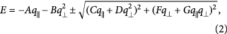
matching perfectly with the DFT results (see red lines in figure 4)10. In the  direction with
  , it reduces to
  , in which the linear dispersions are preserved. In the perpendicular direction with
  , the energy dispersion reduces to
  . The momentum-dependent on-site energy term
  even gives rise to a negative curvature in the bottom conduction band in the energy range of
  eV for square selenene and
  eV for square tellurene (see figures 4(b) and (d)), which corresponds to negative effective mass for the charge carriers.

Figure 3. Top: electronic properties for square selenene: (a) Band structure. Inset: Zoom-in of the band structure in a small region around the semi-Dirac cone at P1 as indicated by a blue box. (b) Band contour for the bottom conduction band (upper panel) and the top valence band (lower panel) in the first BZ. Bottom: ((c) and (d)) corresponding results for square tellurene. SOC is included for all results.
Download figure:
Standard image High-resolution image
Figure 4. Top: low-energy band dispersions around P1 for square selenene in the directions parallel (a) and perpendicular (b) to the  direction. Bottom: ((c) and (d)) corresponding results for square tellurene.
Download figure:
Standard image High-resolution imageDue to the SOC, a considerable band gap Eg is opened at P1 (see blue solid lines in figure 4) with  eV for square selenene and
  eV for square tellurene. The sizes of these band gaps are comparable to that of stanene [10]. This effect can also be considered in equation (1) with the addition of a mass term
  . For square selenene,
  only affects the dispersion very close to P1, and the effective mass for charge carriers in the range of
  eV remains negative in the direction perpendicular to the
  direction. For square tellurene, the SOC band gap significantly alters the dispersion. Calculations with GGA indicate that square tellurene is an indirect band gap semiconductor, while more accurate HSE calculations show that it is a direct band gap material, the same as square selenene11. The features in the band structures along
  are similar to those along
  , but the band gap at the Fermi level at P2 is opened by structural distortion, as the atom in the center of the unit cell is shifted off center along one diagonal direction (see figures 1(c) and (e)).
Both square selenene and tellurene have non-trivial topological properties. Here, we calculate their  invariant from the evolution of the Wannier charge centers (WCC) during an effective adiabatic pumping process [28, 29]. From figures 5(a) and (b), we can see that the WCC bands (black lines) and the reference line (red dash line) only cross once for both systems. Therefore, their
  is 1, indicating that both systems are TIs. One of the most important features of TIs is that they host gapless helical edge states with spin and momentum locked. This is confirmed by our DFT calculations for wide ribbons of selenene and tellurene. Figures 5(c) and (d) show the band structures for zigzag ribbons of selenene and tellurene, with the width being 12.4 nm and 13.9 nm, respectively (see supplemental figure S9). We can clearly see the gapless edge bands (red solid lines) lie in between the bulk band gaps for both systems, confirming their nontrivial topological properties. This is distinctly different from their bulk allotropes in 3D, for which considerable amount of shear strain is required to transform them from trivial semiconductors to TIs [30] or Weyl semimetals [31, 32].

Figure 5. Evolution of the Wannier charge centers (WCC) along kx for square selenene (a) and tellurene (b). a1 is the lattice constant and  . The red dash reference line is only crossed once in both figures, indicating that the Z2 invariant is 1 (non-trivial) for both systems. ((c) and (d)) band structures including SOC near Fermi level for a wide ribbon of square selenene (c) and tellurene (d). The helical edge states are highlighted with red solid lines.
Download figure:
Standard image High-resolution image
Earlier we noted that square selenene and tellurene do not have the lowest cohesive energy among all the 2D structures for Se and Te, respectively. However, when all of them are placed on a substrate, the energy ordering between different structures may change due to substrate effects. Although structures composed of helical chains have the lowest cohesive energy in the gas phase, they tend to obtain less adsorption energy as they are more buckled. On the other hand, with less height variation, square selenene and tellurene may become the most energetically favorable structures on substrates with square symmetry and matching lattice constants. For demonstration, we calculated the formation energy of square tellurene and Te helical chains (rectangular tellurene, see figure 1(d)) on a Au(1 0 0) surface. We found that square tellurene has a formation energy 0.02 eV/atom lower than that of rectangular tellurene, indicating that the former is more energetically favorable to be grown on a Au(1 0 0) surface. More interestingly, when we calculate the atomic structures of Te deposited on a Au(1 0 0) surface from 0.5 monolayer (ML) to 2 ML (see supplemental figure S10), we found that square tellurene is grown layer by layer with the same square pattern on the top surface. This matches nicely with the experimental observation of Ikemiya et al who reported a  pattern for Te deposition on Au(1 0 0) surface with coverages up to 5 ML using high resolution atomic force microscopy (HR-AFM) [33]. A similar situation applies to square selenene: proper substrates satisfying square symmetry and lattice matching conditions are expected to stabilize square selenene instead of other 2D Se structures.
While metal substrates often provide relatively large adsorption energies to stabilize 2D structures, insulating substrates would be desirable as they will preserve the topological properties of the novel square lattices. Indeed, our calculations show that while the topological insulating nature of square tellurene is destroyed when deposited on a Au substrate, it is well preserved on an insulating MgO substrate (see supplemental figure S7). Alternatively, square selenene and tellurene could be grown on metal substrates, and then transferred onto an insulating substrate for further studies using the method discussed by Li et al for silicene [34].
The novel structures we predict here belong to the 2D space group Cm, thus providing realization of TIs in a square lattice with lower symmetry than those discussed by Slager et al for a square lattice in the space group classification of topological band-insulators [35]. These structures also go beyond the simple model discussed by Young et al for Dirac semimetals in 2D [36], because their model is limited to s state electrons, while ours are dominated by p-state hybridizations around the Fermi level. Thus, the special structures predicted here provide a new template for the exploration of other novel Dirac or semi-Dirac semimetals and TIs in 2D [37].
We note that Zhu et al also proposed a few monolayer structures for tellurene recently [38, 39]. Among them, the β structure is the same as the rectangle tellurene we presented in figure 1(b). While the formation of those structures is driven by multivalency nature of Tellurium and may not be applicable to other group VI elements, the structures we predict here are the more common form for 2D elemental materials from group VI.
In conclusion, we report here novel 2D structures for Se and Te, namely, square selenene and tellurene. We confirm their stability with ab initio phonon calculations and MD simulations. We found that they have very interesting electronic structures with two gapped semi-Dirac cones in the square BZ, and they are 2D TIs with non-trivial topological properties. These intriguing properties make them interesting platforms for exploring novel physics and unusual phenomena stemming from the semi-Dirac dispersions and promising materials for 2D electronic and spintronic applications. Finally, using Te on a Au(1 0 0) surface as an example, we demonstrate that they can be grown on proper substrates with square symmetry.
Acknowledgments
We acknowledge financial support from the European Research Council (ERC-2015-AdG-694097), Grupos Consolidados (IT578-13), and COST Action MP1306 (EUSpec). LX acknowledges support from the European Union's Horizon 2020 research and innovation programme under the Marie Skłodowska-Curie grant agreement No. 709382 (MODHET). APP acknowledges postdoctoral fellowship from the Spanish 'Juan de la Cierva-incorporación' program (IJCI-2014-20147). EB acknowledge the support by the National Science Foundation Graduate Research Fellowship under Grant No. (DGE-1450681).
Footnotes
- 7
See supplemental section I for calculational details.
- 8
Furthermore, selenene and tellurene remain stable up to 350 and 400 K, respectively. See supplemental section V.
- 9
The results presented here are calculated with GGA. Calculations with HSE hybrid functional give qualitatively similar results. In particular, the band gaps remain almost the same. See supplemental section III.
- 10
See supplemental table S1 for fitting parameters.
- 11
See supplemental section III for further discussions.