
Abstract
Artificial post-graphene elemental 2D materials have received much attention recently. Especially, stanene, the tin analogue of graphene, is expected to be a robust 2D topological insulator, even above room temperature. We have grown epitaxial 2D stanene on a Ag(1 1 1) single crystal template and determined its crystalline structure synergetically by scanning tunneling microscopy, high-resolution synchrotron radiation photoemission spectroscopy, and advanced first principles calculations. From the STM images, we show that stanene forms a nearly planar structure in large domains. A detailed core-level spectroscopy analysis as well as DFT calculations reveal that the stanene sheet lays over an ordered 2D Ag2Sn surface alloy, but not directly on a bulk-terminated Ag(1 1 1) surface. The electronic structure exhibits a characteristic 2D band with parabolic dispersion due to the non-negligible interaction with the underlying surface alloy.
Export citation and abstract BibTeX RIS

Original content from this work may be used under the terms of the Creative Commons Attribution 3.0 licence. Any further distribution of this work must maintain attribution to the author(s) and the title of the work, journal citation and DOI.
1. Introduction
Post-graphene two-dimensional (2D) elemental honeycomb lattices have received much attention recently [1], because they are expected to host novel striking properties like the quantum spin Hall (QSH) effect [2, 3] and amenability to band gap engineering [4]. Silicene and germanene, such post-graphene materials, had been theoretically predicted by Takeda and Shiraishi in 1994 [5]. In the last years, silicene, germanene, as well as phosphorene and borophene have been successfully grown on Ag(1 1 1), Au(1 1 1), and ZrB2(0 0 0 1) [6–11]. First principle calculations suggest that a silver (1 1 1) surface could be also an ideal candidate for growing large-area, high-quality monolayer stanene [12]. Unique physical properties for stanene have been predicted, such as the QSH effect [13, 14], topological superconductivity [15], giant magnetoresistance [16], perfect spin filter [16], and anomalous Seebeck effect [17]. All these properties are based on low-buckled stanene. Experimentally, there is only one article reporting highly buckled stanene composed of biatomic layers of alpha-Sn(1 1 1), grown on Bi2Te3(1 1 1) [18]. So far, to the best of our knowledge, only one group successfully prepared a low-buckled, 8% compressively strained stanene layer lattice matched to a Sb(1 1 1) substrate with about 20 pm buckling [19]. According to density functional theory (DFT) calculations, low-buckled stanene is identified to be more stable than highly buckled stanene [13]. A planar stanene, functionalized with hydrogen or halogen atoms, has been predicted to show a large-gap QSH state in DFT calculations [20]. The realization of planar stanene requires a small lattice mismatch between stanene and the substrate. DFT calculations indicate that planar stanene is energetically stable on Au(1 1 1)(1 × 1) surface [21]. Experimentally, the clean Au(1 1 1) surface reconstructs into a 22 × √3 superstructure [22]. Therefore, we use a single crystal of Ag(1 1 1) as a substrate, as suggested by Gao et al [12], because the lattice constants of Ag(1 1 1) and Au(1 1 1) are very close and the clean Ag(1 1 1) surface does not form a superstructure.
In this work, we report the epitaxial growth of well-ordered, large area, planar stanene prepared by Sn deposition onto Ag(1 1 1). We examined the crystalline structure using low-energy electron diffraction (LEED), scanning tunneling microscopy (STM), synchrotron radiation core-level spectroscopy (CLS), angle-resolved photoemission spectroscopy (ARPES), along with advanced DFT calculations of the geometry, shallow core-level (CL) chemical shifts, and stability of the system.
2. Experiments and calculations
The experiments were performed using two ultra-high vacuum systems at Nagoya University and at the Aichi synchrotron radiation center. Each system consisted of a preparation chamber with a base pressure below 5 × 10⁻¹⁰ mbar, and an analysis chamber with a base pressure below 10−10 mbar.
Clean Ag(1 1 1) surfaces were prepared by 2 keV Ar+ ion sputtering at room temperature (RT), followed by annealing the sample up to 600 °C. Annealing was performed by electron bombardment of the sample holder at an emission current of 10 mA and a voltage of −650 V. The sample temperature was monitored with a radiation thermometer and a type K thermocouple mounted on the base plate of the sample holder. The cleanliness of the surface was measured by AES after sputtering and annealing; no contaminants, such as C and O, were observed within the detection limits, and a sharp (1 × 1) LEED pattern was observed.
Tin was deposited onto the Ag(1 1 1) surface at various temperatures up to 300 °C in UHV from a well degassed quartz crucible evaporator operating at a deposition rate of approximately 0.05 monolayer (ML) min−1, as measured by placing a quartz crystal microbalance at the sample position. We define 1 ML as a Sn overlayer with the atomic density of a Ag(1 1 1) plane: 1.38 × 10¹⁵ atoms cm−2. The deposition rate was accurately calibrated in advance by Rutherford backscattering spectroscopy (RBS). For the RBS measurement, we prepared a graphite substrate with an ultra-thin tin film on the surface. Details of the experimental setup for RBS have been published elsewhere [23]. The amounts of deposited tin ranged from 0.3 to 1.5 ML; errors in mentioned coverage ratios are less than 5%.
The system was equipped with a rear view LEED system operating with a LaB6 filament and a UHV STM system (Omicron STM-1) at Nagoya University. All STM images presented were acquired at RT with W tips, electrochemically etched in a KOH solution, in constant current mode with positive sample bias voltage (empty states), except a high resolution one taken at a bias of −50 meV (see figure S1 (stacks.iop.org/TDM/5/025002/mmedia)), to show the quite similar appearance of the stanene layer in filled states, because imaging with negative biases turned out to be generally rather unstable. All apparatuses were situated on an air damper with an active vibration isolation system (Kurashiki).
The CLS and ARPES experiments were performed at the Aichi synchrotron radiation center (AichiSR). The system was equipped with a rear view MCP-LEED system and a 200 mm radius hemispherical photoelectron analyzer (MB Scientific AB A-1) with a wide-angle electron lens. The CLS and ARPES spectra were obtained at the sample temperature of 10 K. The overall resolution was better than 50 meV. The silver sample was mounted in a liquid-helium-cooled cryostat with 4-axis pulse motor control.
The ab initio calculations were performed with DFT using the Vienna ab initio simulation package (VASP) [24]. These calculations used the projector augmented wave (PAW) method to describe the interaction between the electrons and ions [25]. The generalized gradient approximation (GGA) was applied throughout this work [26]. Van der Waals corrections were applied following the DFT-D2 method of Grimme [27]. For the calculations of Sn deposited on the Ag substrate, the size of the simulation cell was a = 5.095 Å, b = 5.095 Å and c = 44.017 Å, including a vacuum region larger than 16 Å along the c direction to eliminate artificial interaction between periodic slab images. The Ag substrate was represented by either four or ten atomic layers slab. The top three Ag layers and the stanene were allowed to relax while all the other Ag atoms remained fixed. A plane-wave basis set with energy cutoff of 400 eV was employed. The Brillouin zone of the unit cell was sampled with a 24 × 24 × 1 gamma-center k-point grid. For the calculations of Sn deposited on the Bi2Te3 substrate, carried out for comparison, the size of the simulation cell was a = 4.383 Å, b = 4.383 Å and c = 50.487 Å. A slab consisting of three quintuple-layers (QL) of Bi2Te3 was used to simulate the substrate. The top QL of Bi2Te3 and the stanene layers were allowed to relax and all the other QLs remained fixed. A plane wave basis set with energy cutoff of 600 eV was employed in this case along with a 24 × 24 × 1 gamma-center k-point grid. The forces acting on particular atoms were smaller than 0.01 eV Å−1 in all the structural optimization. Dipole corrections were applied in all the calculations. STM images are simulated based on the Tersoff–Hamann model [28]. Core level shift for the Sn 4d5/2 and Ag 3d5/2 electrons are calculated within the final state approximation [29].
3. Results and discussion
3.1. Successive depositions
3.1.1. √ 3 × √3 Ag2Sn surface alloy at 1/3 monolayer
Figure 1 shows a LEED pattern and experimental STM images of a Ag2Sn surface alloy prepared on a Ag(1 1 1) single crystal with a Sn deposition of 0.33 ML at 200 °C. The LEED pattern, displaying 6-fold symmetry at variance with the 3-fold one of the Ag(1 1 1) substrate, clearly exhibits √3 × √3 spots, as shown in figure 1(a). The wide scale STM image in figure 1(b) shows a single atomic step, 0.24 ± 0.01 nm high, which corresponds to a monoatomic silver step, separating two wide terraces without any evidence of two- and 3D islands. The average width of the terraces is, typically, more than 200 nm. The high-resolution STM image in figure 1(c) clearly shows only one bright protrusion per √3 × √3 unit cell. These results confirm the previous report by Osiecki et al that a Ag2Sn surface alloy is formed with √3 × √3 periodicity upon Sn deposition of 1/3 ML onto the Ag(1 1 1) kept at 200 °C [30].
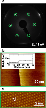
Figure 1. (a) LEED pattern at 41 eV incident electron energy of a Ag2Sn surface alloy prepared on a Ag(1 1 1) single crystal at a Sn coverage of 0.33 ML. √3 × √3 spots are marked in the image. (b) Large-scale and (c) close-up STM images of the Ag2Sn surface alloy. The images are recorded in a constant current mode with tunneling current of 200 pA and sample bias voltage of +1 V and +0.3 V, respectively. A line profile in (b) gives a step height of 0.24 ± 0.01 nm, pointing to a Ag(1 1 1) monoatomic step. A √3 × √3 unit cell is drawn in (c).
Download figure:
Standard image High-resolution image3.1.2. Formation of stanene, with 0.5 monolayer added on top of the √3 × √3 surface alloy
Figure 2(a) shows experimental STM images of the Sn film deposited onto the Ag2Sn surface alloy for an additional 0.5 ML at 150 °C. We find that the film grows two dimensionally on this Ag2Sn surface alloy, possibly from the substrate steps, with large domain areas of, typically, 5000 nm2. The films adopt a layer-by-layer growth and 3D islands are not observed. The corresponding LEED pattern exhibits only √3 × √3 spots, as shown in figure 2(b), again with 6-fold symmetry, yet, their intensities at different energies, differ significantly from those of the initial Ag2Sn surface alloy, which allows easy distinction. The section profiles indicate that step heights are 0.25 ± 0.01 nm (figure 2(c)). Close-up STM images clearly reveal a striking honeycomb structure (figure 2(d)). The section profile indicates that the height difference between Sn atoms is within 5 pm only (figure 2(e)), while the high-resolution STM image shows that there is no periodicity in the height within the unit cell, at variance with the case of graphene with its two strictly equivalent A and B sub-lattices (figure 2(f)). It is thus inferred that a nearly perfect planar layer is formed, growing in a 2D island mode on the initial Ag2Sn surface alloy. The fast Fourier transform (FFT) image calculated from figure 2(d) clearly shows periodic spots (figure 2(g)). Instead, the STM image from the uncovered part of the Ag2Sn surface alloy area exhibits just a single bright protrusion per √3 × √3 unit cell (figure 2(h)), as expected from the results mentioned above (figure 1). Therefore, it is concluded that almost perfect planar stanene is formed on the Ag2Sn surface alloy.

Figure 2. Stanene prepared either on a Ag2Sn surface alloy or straightly on a clean bare Ag(1 1 1) single crystal. (a) Large-scale STM image of stanene prepared on a Ag2Sn surface alloy upon post Sn deposition of 0.5 ML at 150 °C. The image is recorded in constant current mode with tunneling current of 1.0 nA and sample bias of +1.0 V. (b) LEED pattern at 41 eV incident electron energy for stanene prepared on the Ag2Sn surface alloy. (c) Sectional profiles along the (A)–(D) lines in (a). (d) High-resolution STM image of stanene: a zoom-in on the red-line square in the top part of (a): Us = +0.005 V, I = 300 pA, empty states. The honeycomb stanene structure model is superimposed. (e) Sectional profile along the (E) and (F) line in (d). (f) Close-up STM image of (d) top part. (g) FFT image of (d). (h) High-resolution STM image of the Ag2Sn surface alloy, which is observed in the green line square in (a) (Us = +0.3 V, I = 200 pA). (i) Large-scale STM image of stanene prepared straight on Ag(1 1 1) with Sn deposition of 0.9 ML at 150 °C (Us = +1.0 V, I = 1.0 nA). The inset of (i) is a high-resolution STM image of the stanene layer (Us = +0.005 V, I = 300 pA). (j) LEED pattern at 41 eV incident electron energy of stanene prepared straight on Ag(1 1 1). The √3 × √3 LEED spots are marked in the images.
Download figure:
Standard image High-resolution image3.2. Stanene formation upon uninterrupted deposition onto bare Ag(1 1 1)
Figure 2(i) shows experimental STM images of a Sn film deposited straight onto a clean bare Ag(1 1 1) for 0.9 ML at 150 °C. We find that the film grows two dimensionally and a close-up STM image clearly reveals a honeycomb structure, indicating an apparent coverage of only 2/3 ML, as if just a sole silicene sheet, instead of the actual 0.9 ML one. The LEED pattern exhibits √3 × √3 spots only, as shown in figure 2(j). These experimental facts, very similar to those obtained in the previous successive deposition procedure, indicate that the stanene film grown upon uninterrupted Sn deposition onto the clean Ag(1 1 1) also developed past the formation of an initial Ag2Sn surface alloy with nominal 1/3 ML coverage. Further confirmation of these results has been obtained through synchrotron radiation CLS and DFT calculations, as described below.
3.3. CL measurements
To study the growth of stanene on Ag(1 1 1) in more details, we used synchrotron radiation CLS of the shallow Sn 4d and Ag 3d CL's in highly surface sensitive conditions. The high-resolution Ag 3d5/2 spectrum of the bare silver (1 1 1) single crystal template is displayed in figure 3(a). The high-resolution Sn 4d and Ag 3d5/2 spectra of a Ag2Sn surface alloy prepared on the silver (1 1 1) substrate are shown in figures 3(b) and (e), respectively, while those for the stanene sheet grown on top of the surface alloy at 150 °C are displayed in figures 3(c) and (f), respectively. The Sn 4d full width at half maximum (FWHM) for stanene grown on the surface alloy is 0.41 eV, which is much broader than that for the Ag2Sn surface alloy (0.27 eV). A thorough decomposition indicates that there are two components, namely S1 and A2, separated by 0.17 eV, with an intensity ratio for S1 to A2 of 2 to 1. Because the high-resolution STM images exhibit essentially a planar honeycomb structure, one of the components of the Sn 4d CL's clearly originates from the stanene layer, while the other component is attributed to the Ag2Sn surface alloy covered with the stanene overlayer. From the intensity ratio, the S1 and A2 components are unambiguously associated to the stanene sheet and the Ag2Sn surface alloy, respectively. We also measure the CL's for the straight deposition of 0.8 ML of Sn onto the clean Ag(1 1 1) surface at 150 °C, as shown in figures 3(d) and (g). Clearly, the Sn 4d and Ag 3d5/2 CL shapes for both types of preparations are very similar, indicating a close relation between the two growth fashions. That is, during the uninterrupted deposition of Sn onto the clean Ag(1 1 1) surface, the Ag2Sn surface alloy may form first [30] and the continued deposition of Sn leads to the formation of a stanene layer on top. To summarize at this point, the presence of a purely Sn topmost layer is justified by the emergence of two components in the Sn 4d CLs, where one is related to the interfacial Ag2Sn and the other one necessarily to another, different Sn-based layer. We note that a Ag2Sn double layer (with no stanene) could be qualified, instead, by a single Sn component. As such, the 'other Sn-based layer' can be attributed to pure Sn elemental bonding, that is, undoubtedly to a stanene sheet, as evidenced in the honeycomb STM images.

Figure 3. High-resolution synchrotron radiation Sn 4d and Ag 3d5/2 CL spectra measured at 10 K and taken at hν = 70 eV and 430 eV, respectively. (a) Ag 3d5/2 for a clean bare Ag(1 1 1) single crystal, (b) and (e) Sn 4d and Ag 3d5/2 for a Ag2Sn surface alloy at a Sn coverage of 0.33 ML, (c) and (f) Sn 4d and Ag 3d5/2 for stanene prepared on a Ag2Sn surface alloy with post Sn deposition of 0.5 ML at 150 °C, (d) and (g) Sn 4d and Ag 3d5/2 for stanene prepared by straight deposition of 0.9 ML onto bare Ag(1 1 1) at 150 °C. S1, A, I, are the components related to stanene, the surface alloy, the interface, while SAg, and B correspond to the Ag surface component, and the Ag bulk one at 368.1 eV binding energy (pinpointed by the vertical line), respectively. Each suffix number represents the layer number from top to down.
Download figure:
Standard image High-resolution imageThe comparison and decompositions of the Ag 3d5/2 spectra for the clean bare Ag(1 1 1) surface (figure 3(a)), the Ag2Sn surface alloy (figure 3(e)), the stanene layer prepared on the Ag2Sn surface alloy (figure 3(f)), and that prepared by straight deposition onto the bare Ag(1 1 1) surface (figure 3(g)) confirm this scenario. The spectra for the Ag2Sn surface alloy and the differently prepared stanene layers exhibit similar FWHMs and are just slightly broader than the spectrum from the clean bare Ag(1 1 1) surface, which comprises a surface component, SAg, in addition to the bulk component B. For the Ag2Sn surface alloy itself, three components are needed for the fit, related to silver in the Ag2Sn surface alloy (A1), to the silver layer beneath the surface alloy (I2), and, to the bulk component (B), indeed located at the same binding energy in all cases of figures 3(a)–(g). Once the initially formed Ag2Sn surface alloy is covered with the stanene layer (either for the interrupted or straight growth procedure), the original A1 and I2 components shift slightly to higher binding energy because of the different environment, and are re-named as A2 and I3 components. Correlatively, the intensity of the B component decreases because of the short electron escape depth at the very surface sensitive measurement conditions used.
Therefore, the Ag 3d5/2 spectrum is considered to comprise three components stemming from the Ag2Sn surface alloy (A2), from the silver layer beneath the surface alloy (I3), and from the bulk component (B). Hence, from the synchrotron radiation CLS detailed signatures, in synergy with the STM images and the different intensities noticed in the LEED patterns (see above), we can unambiguously conclude that stanene with a planar honeycomb structure has been formed in both cases on top of an Ag2Sn surface alloy.
3.4. theoretical insights
In order to understand deeper our experimental results, we performed DFT calculations for various Sn configurations on top of the Ag(1 1 1) surface in a √3 × √3-Ag supercell. Table 1 shows the formation energy of different configurations, defined as Ef = (Etot − Esub)/NSn − ESn (without surface alloy) or Ef = (Etot − Esub − EAg × NAg)/NSn − ESn (with the surface alloy), where Etot is the total energy of the combined system, Esub is the total energy of the clean Ag substrate without Sn structures or the surface alloy layer, ESn is the total energy of an isolated Sn atom, NSn is the total number of the Sn atoms and NAg is the number of Ag atoms in the alloy layer(s). These calculations show that the Ag2Sn surface alloy is energetically the most stable phase among all the studied configurations, indicating that the Ag2Sn surface alloy will first form upon deposition of Sn onto the clean Ag(1 1 1) surface. We further emphasize that among all the configurations with the Ag2Sn surface alloy, stanene on the Ag2Sn surface alloy is the most stable one, indicating stanene will grow subsequent to the formation of the surface alloy. The optimized structure for stanene on the Ag2Sn surface alloy with the calculation method used (vdw-D3 correction and GGA pseudopotential) results in a nearly flat surface in a honeycomb arrangement with maximum height variations of less than 0.12 Å, in very good agreement with the experimental observations, and Sn atoms located at bridge sites (one above Ag–Ag and the other above Ag–Sn on top of the surface alloy), as shown in the simulated STM image (figure 4(b)). The calculated step height between the stanene layer and the underlying Ag2Sn surface alloy is 0.26 nm, also consistent with the experimental results. The practically flat geometry of stanene obtained here is different from the significantly buckled one (by 1.06 Å) reported in a comparable theoretical study [31], in which the authors adopted the lattice constant of free-standing stanene and artificially compressed the Ag lattice, resulting in a buckled geometry. This results from the flexibility of the bond angles within the stanene sheet, due to the intrinsic buckling: the stanene sheet is compliant to its substrate to favor the epitaxial matching.
Table 1. DFT calculation results for different Sn structures on silver (1 1 1) slabs, with van der Waals interactions (vdw) for several different types of model.
| Structure | Formation energy per Sn atom (eV) |
|---|---|
| Ag2Sn surface alloy | –4.27 |
| Stanene on Ag2Sn surface alloy | –3.88 |
| Hexagonal close packed Sn layer on Ag2Sn surface alloy | –3.76 |
| Single Sn atom on Ag2Sn surface alloy | –3.75 |
| Bilayer stanene on Ag2Sn surface alloy | –3.70 |
| Hexagonal close packed Sn layer directly on clean Ag(111) | –3.53 |

Figure 4. Structural models (side and top views) and their simulated STM images of (a) Ag2Sn surface alloy and (b) stanene on Ag2Sn surface alloy.
Download figure:
Standard image High-resolution imageThe calculated Sn 4d CL's for stanene on the Ag2Sn surface alloy shows two components (table 2), one originating from the stanene layer and the other from the surface alloy, corresponding to the S1 and A2 components measured in the experiments. The calculated binding energy difference between S1 and A2 components is 0.16 eV, also matching well with the experimental value. The calculated Ag 3d5/2 CLS spectrum for stanene on the Ag2Sn surface alloy is composed of three components, as found in experiments. The Ag 3d5/2 chemical shifts for the second layer Ag2Sn surface alloy (A2 component) and from the silver layer beneath the surface alloy (I3) were calculated to be 0.54 eV and 0.18 eV toward higher (BE) with respect to that for Ag bulk. These values are consistent with the chemical shifts and respective intensities obtained through our CL decomposition analysis. In fact, with the constraint of the small supercell size (the √3 × √3 Ag supercell) determined by the LEED observations, the possible configurations matching with the experimental CLS results (two components for Sn and three components for Ag) are very limited. The perfect agreements between the theoretical and the experimental CLS spectrum and STM results constitute compelling evidence that the structure observed in experiments is a flat stanene layer on the Ag2Sn surface alloy.
Table 2. Calculated step heights and CL shifts for Sn 4d5/2 and Ag 3d5/2 of the clean Ag(1 1 1) surface, the Ag2Sn surface alloy, and the stanene sheet on the Ag2Sn surface alloy.
| System | Step height (nm) | CL shifts (eV) |
|
|---|---|---|---|
| Sn 4d5/2 | Ag 3d5/2 | ||
| Clean Ag surface | 0.24 | — | 0.00 (B), −0.14 (S) |
| Ag2Sn surface alloy | 0.26 | 0.00 | 0.15 (A1), 0.04 (I2), 0.00 (B) |
| Stanene on Ag2Sn surface alloy | 0.26 | 0.16 (A2), 0.00 (S1) | 0.54 (A2), 0.18 (I3), 0.00 (B) |
aThe majority component of Sn 4d5/2 and the bulk component of Ag 3d5/2 are set to 0.00 eV as the reference energy.
The interaction between the stanene layer and the underlying Ag2Sn surface alloy is relatively strong. Therefore, the stanene layer is flattened to maximize the adsorption energy, and the lattice constant is expanded (with ~10% strain) compared to that of spontaneously buckled freestanding stanene. We note that a very similar expansion was obtained in the case of germanene grown on Au(1 1 1) [8]. If we define the absorption energy of the stanene layer as Ead = (Esub − Estan)/Nsn, where Esub is the total energy of the substrate (i.e. clean Ag(1 1 1), Ag2Sn surface, etc), Estan is the total energy of the stanene layer and Nsn is the number of tin atoms in the stanene layer, then the calculated formation energy of the stanene layer in this system is 3.88 eV, much larger than the cohesive energy of bulk Sn (grey tin) with a value of 3.50 eV/atom. The relatively strong interaction between stanene and the surface alloy gives rise to the nice uniformity of the overlayer and facilitates the 2D growth of stanene in large areas.
For comparison with the first realization of highly buckled stanene on Bi2Te3 [18], we calculated also the adsorption energy of stanene on Bi2Te3; in contrast, it is only 3.14 eV/atom, which is even smaller than that of bilayer stanene on the same substrate by 0.10 eV/atom, and that of bulk Sn by 0.36 eV/atom. Therefore, bilayer and multilayer islands could easily form during the growth of stanene on Bi2Te3 and it would be relatively difficult to maintain a good uniformity of the sample.
3.5. Electronic band structure
In order to identify the electronic band structure of our epitaxial stanene, the band structures of the Ag2Sn surface alloy, and that of a stanene sheet on top were examined by ARPES at a photon energy of 70 eV, as displayed in figures 5(a) and (b). The band structure related to the surface alloy is clearly recognized with a typical Λ-shape around the Brillouin zone center (Γ point), as it has been previously determined [30]. For stanene on the Ag2Sn surface alloy, the band structure exhibits a parabolic dispersion around Γ. This parabolic band does not disperse with the photon energy (see figure S2), i.e. with  , the perpendicular momentum, which ascertains its 2D character; it is directly related to the stanene-on-surface alloy association. The effective mass m* is 0.55 me, where me is the electron rest mass, as calculated by parabola curve fitting, and the Fermi velocity is quite high, namely, 1.27 × 10⁶ m s−1. As shown in the supplement (figure S3), the calculated parabolic bands near the Γ point resemble that experimentally obtained, to which it may correspond. However, the minimum is shifted by 1.25 eV, which may be due to local structural changes, indeed, not taken into consideration, as well as many body effects, also not taken into account in the calculations. A constant energy map obtained within an interval of ±0.05 eV at just 0.05 eV below the Fermi level reveals a circular cross-section, as shown in figure 5(c). The parabolic band thus appears to be, in the vicinity of the Fermi level, as isotropic.

Figure 5. (a) ARPES intensity plot of the Ag2Sn surface alloy prepared on a Ag(1 1 1) single crystal at a nominal Sn coverage of 0.33 ML, and (b) ARPES intensity plot of stanene prepared on the Ag2Sn surface alloy with post Sn deposition of 0.5 ML at 150 °C, measured along the K–Γ–K direction with hν = 70 eV at 10 K. (c) Constant energy contour obtained within an interval of at ±0.05 eV at just 0.05 eV below the Fermi level for stanene on the Ag2Sn surface alloy. The large hexagon represents the 1 × 1 Ag(1 1 1) surface Brillouin zone, while the smaller ones correspond to the √3 × √3 R (30°) structure related to stanene.
Download figure:
Standard image High-resolution image
Although it is determined that stanene with a planar honeycomb structure is formed on top of an Ag2Sn surface alloy, ARPES measurements only reveal a parabolic band structure without any indication of Dirac cone. A strong interaction between stanene and metal substrates has been already reported [31]. The Dirac band structure of free-standing stanene may be destroyed for the present system of epitaxial stanene on a Ag2Sn surface alloy. However, further experimental and theoretical studies, may reveal still unnoticed enticing properties, such as the actual presence of interaction induced Dirac cones at previously insufficiently explored regions of the band structure, as has been revealed recently for epitaxial silicene on Ag(1 1 1) [32, 33], which was considered before as loosing its most exciting properties [34]. We also recall that structural flatness of stanene is predicted to drive RT QSH effects [19].
Last but not least, we foresee no major obstacle to remove the stanene sheet from its silver substrate, as has been successfully realized for the fabrication of the first field effect transistors (FETs) with a single-layer silicene channel using the smartly devised process named silicene encapsulated delamination with native electrodes [35, 36]. With the same procedure, possibly, the QSH effect could be even electrically demonstrated.
4. Conclusion
In summary, we have successfully prepared planar stanene for the first time. We used a Ag(1 1 1) crystal as a substrate and examined the in situ epitaxial growth, with the impinging Si flux precisely controlled by Rutherford backscattering, by high-resolution STM imaging, synchrotron radiation CL and angle-resolved photoelectron spectroscopies. The experimental results, showing evidence of the unprecedented realization of large area planar stanene on an underlying Ag2Sn surface alloy, have been supported by thorough density functional calculations. A parabolic 2D band structure around the Brillouin zone center has been observed, possibly indicating an interfacial 2D band. Planar stanene, a novel tin allotrope akin to graphene, is considered to be the most promising 2D topological insulator hosting the QSH effect, even markedly above RT. As tin already fits nicely with the ubiquitous silicon technology, planar stanene, possibly with further functionalization, for which the same procedure used to realize the first silicene FETs can be envisaged, appears as a highly promising electronic material. Thence, we have added a larger spin–orbit coupling elemental group IV cousin to silicene and germanene, which opens enticing perspectives, especially for nanoelectronics, spintronics, and for potential quantum computing applications.
Acknowledgments
The authors are grateful to Prof K Soda of Nagoya University Synchrotron Radiation Research Center and Dr Y Watanabe and Dr A Nozaki of AichiSR for experimental supports. This work was partially supported by a Grant-in-Aid for Scientific Research (B) (No. 15H03677) and (C) (No. 22560022) from the Japan Society for the Promotion of Science (JSPS). The CLS and ARPES experiments were conducted at the BL7U of Aichi Synchrotron Radiation Center, Aichi Science & Technology Foundation, Aichi, Japan with the financial support of Synchrotron Radiation Research Center, Nagoya University (no. 2017001). AR and LX acknowledge financial support from the European Research Council (ERC-2015-AdG-694097), Grupos Consolidados (IT578-13), and European Union's H2020 program: GA no. 676580 (NOMAD) and GA no. 646259 (MOSTOPHOS). LX acknowledges support from the European Union's Horizon 2020 research and innovation programme under the Marie Skłodowska-Curie grant agreement no. 709382 (MODHET). GLL acknowledges support from Nagoya University thanks to an 'Eminent Foreign Scientist' Invitation Award in 2015/2016, as well as an Invitational Fellowship for Research in Japan by the Japan Society for the Promotion of Science (JSPS) in 2017.