
Abstract
We have measured the two-dimensional image potential states (IPS) of a germanene layer synthesized on a Ge2Pt crystal using scanning tunnelling microscopy and spectroscopy. The IPS spectrum of germanene exhibits several differences as compared to the IPS spectrum of pristine Ge(001). First, the n = 1 peak of the Rydberg series of the IPS spectrum of germanene has two contributions, labelled n = 1- and n = 1+, respectively. The peak at the lower energy side is weaker and is associated to the mirror-symmetric state with opposite parity. The appearance of this peak indicates that the interaction between the germanene layer and the substrate is very weak. Second, the work function of germanene is about 0.75 eV lower in energy than the work function of Ge(001). This large difference in work function of germanene and pristine Ge(001) is in agreement with first-principles calculations.
Export citation and abstract BibTeX RIS

Original content from this work may be used under the terms of the Creative Commons Attribution 4.0 license. Any further distribution of this work must maintain attribution to the author(s) and the title of the work, journal citation and DOI.
1. Introduction
Two-dimensional image potential states (IPS) are unoccupied electronic states that are trapped in a potential well in front of a surface. The potential well is formed by the surface projected bulk bandgap and the image potential barrier arising from the interaction between an electron near the surface and its positive image charge. The electrons in these 2D states have a free-electron like dispersion parallel to the surface and are confined in the perpendicular direction. The confinement in the direction normal to the surface results in a Rydberg-like series of peaks below the vacuum level [1–3]. The IPS can be measured by several techniques including inverse photoemission and two-photon photoemission [4], low energy electron diffraction [5] and scanning tunnelling microscopy (STM) [6–9]. In STM the electric field in the tunnel junction modifies the electrostatic potential and the IPS peaks are shifted to higher energies. If the IPS peaks exceed the vacuum level, we enter the field emission resonance regime. Therefore, the series of peaks are sometimes referred to as field emission resonances or Gundlach oscillations [10]. The investigation of these electronic states provides important information concerning the charge injection and the dynamics of charges on surfaces, the dissipation behaviour on topological insulators [11], induced light emission [12, 13], influence of the electric field on electron dynamics [14, 15], electronic effects of the surface potential corrugation [16], variations of the work function [17–19], quantum bit interactions [20] and quantum dot behaviour of graphene nano-islands [21]. In addition, using STM IPS spectroscopy it is also possible to obtain atomic resolution on diamond [22].
For a free-standing 2D material, theory predicts the occurrence of two mirror-symmetric Rydberg series of IPS exhibiting opposite parity with respect to the reflection plane of the 2D material [23]. The hybridization of these double series of states between the successive graphene layers in graphite produces the so-called interlayer states [24], which play a key role in the superconducting properties of alkali intercalated graphite [25]. When single and bilayer graphene are grown on SiC the first pair of the mirror-symmetric double Rydberg series persist, indicating a weak coupling of graphene with the underlying substrate [26]. When graphene is grown on metallic substrates, the double parity Rydberg-like series of IPS of the free-standing graphene evolves towards a single series. This is due to the repulsion between both materials and the reduction of the mirror symmetry of the free-standing graphene layer. The latter even holds for the weakly interacting regime where the separations between graphene and metal are relatively large [27]. However, for strong interactions and thus small graphene-metal separations [28] IPS spectra reveal the formation of a graphene-metal interfacial state [29]. Moreover, IPS spectra provide very accurate information on the work function of a material. For instance, IPS measurements using STM of a graphene/metal system show a lateral modulation of the work function due to the modulated graphene/substrate interaction [29]. Furthermore, IPS studies of graphene and h-BN grown on Ag [30] reveal a difference in their work functions [31].
While several STM measurements of IPS and work function variations were performed on different graphene systems, to our knowledge no such studies were reported on 2D-Xenes [32] of the group 14 elements of the periodic table. The silicon, germanium and tin analogues of graphene are referred to as silicene, germanene and tinene or stanene, respectively. These 2D materials share many properties with their carbon counterpart [33–37]. There are, however, also a few differences between the 2D-Xenes and graphene. The honeycomb lattice of the 2D-Xenes is buckled, whereas graphene's honeycomb lattice is planar. Furthermore, 2D-Xenes have a larger spin–orbit coupling than graphene because the atomic number of Si, Ge and Sn is larger than that of C. Unfortunately, silicene, germanene and stanene do not occur in nature and therefore they have to be synthesized.
Here we will measure the two-dimensional IPS of germanene synthesized on Ge2Pt crystals. We will compare the IPS spectrum and work function of germanene with pristine Ge(001). In order to validate our experimental observations, we will also perform density functional theory calculations. The analysis of the n = 1 state of the germanene IPS spectrum as well as the spectroscopic features at energies below the n = 1 IPS peak will provide important information on the coupling of the germanene to the underlying substrate.
2. Methods
2.1. Experimental details
The image potential states have been measured with a low-temperature scanning tunneling microscope under ultra-high vacuum (UHV) conditions at 77 K. The base pressure of the UHV system was in the range of 1 × 10⁻¹¹ mbar. The germanium (Ge) (001) substrates were cut from nominally flat single side polished and slightly doped n-type samples. In order to avoid contamination of the Ge(001) substrates, only sample holders that were composed of molybdenum, tantalum or aluminium oxide have been used. The samples were cleaned by cycles of 500–800 eV argon ion bombardment and annealing at 1100 K [38]. After several cycles the Ge(001) substrates exhibited a well-ordered c(4×2) dimer-row reconstruction and monolayer high atomic steps at 77 K. Subsequently, we have deposited a few monolayers of platinum (Pt) on some of our Ge(001) samples by heating a 99.997% purity platinum (Pt) wire wrapped around a tungsten filament. After Pt deposition the Ge(001) sample was annealed at a temperature above the eutectic temperature (1040 K) of the Pt-Ge alloy. This resulted in the formation of Pt0.22Ge0.78 eutectic droplets. Upon cooling down the Ge(001)/Pt system to temperatures below the eutectic temperature these droplets undergo spinodal decomposition into a pure Ge phase and a Ge2Pt alloy. The clusters found at room temperature are composed of a Ge2Pt core decorated with a germanene shell [39, 40]. A detailed description of the growth studies of germanene on Ge2Pt prepared on Ge(001) is presented in the Supporting Information (available at stacks.iop.org/TDM/7/035021/mmedia). The z(V) spectroscopy experiments were performed in the constant current mode, recording the tip-surface distance while varying the bias voltage, and averaging multiple curves acquired at different positions on the surface. The dz/dV curves are the numerical derivatives of the z(V) traces. The I(V) measurements were performed using a lock-in amplifier with a modulation voltage of 20 mV and a frequency of 1.7 kHz.
2.2. Computational details
The density functional theory (DFT) calculations were made using the projected augmented wave (PAW) formalism [41] as implemented in the Vienna ab initio simulation package (VASP) [42, 43]. The exchange-correlation effects were taken into account by using the generalized gradient approximation [44]. A 600 eV energy cutoff for the plane-waves and a convergence threshold of 10–7 eV were used. In order to avoid interactions between the cells, a 30 Å thick vacuum slab was added in the direction normal to the germanene sheet. The Brillouin zone was sampled by a (32×32) k-point mesh. The work function was estimated as a difference between the vacuum potential and the Fermi energy.
3. Results and discussion
3.1. Germanene/Ge2Pt and Ge(001)-c(4×2)
In figures 1(a) and (b) scanning tunneling microscopy images, dI/dV and dz/dV spectra of pristine Ge(001)-c(4×2) and germanene grown on a Ge2Pt crystal are shown. At cryogenic temperatures the dimer rows of Ge(001) are buckled. Adjacent dimers within a dimer row buckle in opposite directions resulting in zigzag rows (see figure 1(a)). Adjacent dimer rows can buckle in-phase or out-of-phase resulting in a p(2×2) or c(4×2) reconstruction, respectively. Here we have focussed on regions with a c(4×2) buckling registry as these regions are more abundant than the p(2×2) regions. In addition, at sample biases exceeding the edge of the conduction band p(2×2) domains are often converted to c(4×2) domains [38, 45]. The nearest neighbor distance between dimers and dimer rows are 4 Å and 8 Å, respectively. A structural model of the c(4×2) reconstructed phase is shown in the left panel of figure 1(a). In the middle panel a dI/dV spectrum of Ge(001) is shown. The spectrum shows a bandgap, which is somewhat smaller than the bulk bandgap owing to the presence of surface states in the forbidden zone.
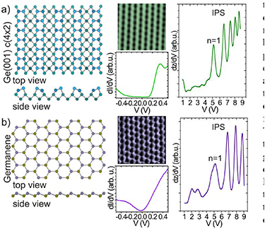
Figure 1. (a) Ge(001)-c(4×2) surface. Left panel: structural model of the reconstructed Ge(001) surface with buckled dimer rows. Adjacent dimer rows buckle in an out-of-phase registry. Middle panel: STM image (5 nm x 5 nm) and dI/dV spectrum of Ge(001). Right panel: dz/dV curve showing the IPS spectrum of Ge(001)c-(4×2). (b) Germanene grown on a Ge2Pt crystal. Left panel: structural model of buckled honeycomb lattice of germanene. Middle panel: STM image (5 nm x 5 nm) of germanene and V-shaped dI/dV spectrum. Right panel: dz/dV curve showing the IPS spectrum of germanene.
Download figure:
Standard image High-resolution imageGermanene has a buckled honeycomb structure with a lattice constant slightly larger than 4 Å. The buckled honeycomb lattice is composed of two triangular sub-lattices that are slightly displaced with respect to each other in a direction normal to the germanene sheet (see the structural model in the left panel of figure 1(b)) [39]. Owing to this buckling one of the triangular sub-lattices shows up more prominently than the other triangular sub-lattice. We should emphasize here that the electric field of the STM can result in a charge transfer from one triangular sub-lattice to the other triangular sub-lattice. The latter leads to a decrease of the spin-orbit bandgap and for sufficiently large electric fields even to full closure followed by a reopening of the bandgap [40, 46]. The differential conductivity (dI/dV), which is proportional to the density of states, displays a characteristic V-shape for germanene (see figure 1(a) middle panel). This V-shaped density of states is one of the hallmarks of a two-dimensional Dirac material [34–37]. The germanene is lightly n-doped as the charge neutrality is located at negative energy with respect to the Fermi level. In principle one would expect to see a difference between the dI/dV spectra of the two sub-lattices of germanene. Our experiments, however, do not reveal this spatial variation, which we ascribe to the relatively small buckling of only 0.2 Å [39].
In the right panels of figures 1(a) and (b), dz/dV curves are shown for Ge(001) and germanene, respectively. For both surfaces several well-defined oscillations are observed when the applied bias voltage exceeds the work function of the substrate. These oscillations are the IPS resonances in the triangular potential well formed between the substrate and the STM tip. The IPS spectra of Ge(001)-c(4×2) and germanene show some differences: (i) The oscillations of the pristine Ge(001)-c(4×2) substrate occur at different energies than the oscillations of the germanene layer; (ii) A larger number of oscillations are observed for Ge(001)-c(4×2) than for germanene; (iii) The exact shape of the IPS n= 1 peak, observed at around 5 V, has a symmetric and well-defined appearance for Ge(001)-c(4×2), whereas for germanene the IPS n= 1 peak is asymmetric and can be decomposed into two peaks; (iv) At energies smaller than 5 eV, several well-defined spectroscopic peaks occur for germanene, which are absent for Ge(001)- c(4×2). In order to explain these differences, a detailed analysis and comparison of the IPS spectra of germanene and Ge(001)-c(4×2) is presented in the following section.
3.2. 2D- IPS and work function of Germanene/Ge2Pt and Ge(001)-c(4×2)
The local work function and the IPS oscillations of Ge(001)-c(4×2) and germanene grown on Ge2Pt crystals were measured using z(V) spectroscopy. In case that the sample bias coincides with one of the IPS states the z-piezo retracts in order to maintain a constant tunnel current. This is because IPS states correspond to standing electron waves in the triangular shaped potential well between substrate and tip.
In the dz/dV curves, the IPS appear as successive peaks at energies above the work function (see figure 2). The spectra were measured for different set point values of the tunnel current (figures 2 (a) and (b)—left panels). A shift to higher energies of the IPS peaks positions with increasing set point current is a typical feature caused by the higher electric field in the tunnel junction. It should be noted that the spectral features, i.e. the energy and the shape of the peaks, are different for Ge(001)-c(4×2) and germanene. This difference can be explained partly by a difference in the work function [17–19, 29–31] of the two materials.
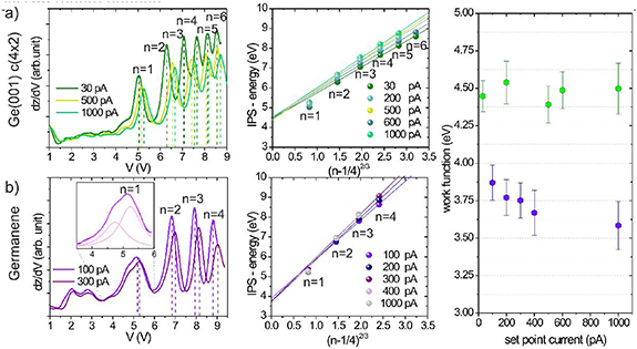
Figure 2. (a)-(b) IPS spectra measured on Ge(001)-c(4×2) and on germanene grown on Ge2Pt, respectively. Left panels: dz/dV curves acquired at different tunnel current set points. The energies of the IPS are marked with vertical dashed lines. Ge(001)-c(4×2) has more IPS peaks than germanene. Inset (b): First n = 1 IPS of germanene fitted with 2 Lorentzian peaks. Middle panels: Gundlach fits of the IPS energies, i.e. energy versus (n-1/4)2/3. The intercept provides the work function. Right panel: Work function of Ge(001)- c(4×2) and of germanene, measured at different set points.
Download figure:
Standard image High-resolution imageMoreover, the number of observed IPS peaks is also different for the two materials. This can be ascribed to a different shape of the potential well for the two systems. The energy values En of the IPS peaks were obtained by fitting the dz/dV spectra to a series of Lorenzian profiles and were plotted in the middel panels of figures 2 (a) and (b). By fitting the IPS peaks with a (n-1/4)2/3 dependence [10], where  , with φ the work function and F the electric field. In the fit we considered the high order peaks (n > 1), since these peaks are less influenced by the interaction with the substrate [19]. Accordingly, we obtained an average work function of 4.48 ± 0.20 eV for Ge(001)-c(4×2) and 3.73 ± 0.55 eV for germanene. The work function of Ge(001)-c(4×2) agrees well with available experimental data [47, 48]. Since no experimental data is available for free-standing germanene, we have performed density functional theory calculations for germanene. Using a lattice constant of 3.82 Å and a buckling of 0.86 Å [37] a work function of 4.1 eV was found. The calculated value of the work function of 4.1 eV is slightly larger than the value of 3.73 eV that was extracted from the IPS analysis. The work function values were plotted for both materials in figure 2—right panel, as a function of the tunnel current set point. The apparent shift of the work function of germanene towards lower values may be related to the strong influence of the electric field on the germanene layer [15, 49, 50, 51]. The electric field will also affect the shape of the potential well between the germanene layer and the STM tip.
Furthermore, striking differences in the IPS spectra of germanene and Ge(001)-c(4×2) are observed at energies below the n= 1 IPS peak (figures 2(a) and (b) left panels). While the weak wrinkles in the curve of Ge(001)-c(4×2) are related to the electronic variations in the conduction band, the interpretation of the multiple peak-like features in the spectra of germanene can be explained by two opposing scenarios.
1) The interaction of the germanene layer with the substrate is strong, which can result in the formation of interfacial states [27, 29, 49, 50]. As an example of such a system we refer to graphene/Ru(0001) [29, 50]. Moreover, these interfacial states could also affect the first IPS peak. The decomposition of the n= 1 peak into two peaks might be induced by the interfacial states (figure 2(b)-left panel).
2) The interaction of the germanene layer with the substrate is very weak. We anticipate that our germanene system is, at least to some extent, similar to graphene on SiC. For the graphene on SiC Bose et al [26] observed the two mirror-symmetric n= 1 peaks for graphene as well as bilayer graphene on SiC. The energy separation of these two n= 1 peaks is larger for graphene as compared to bilayer graphene. In fact, the bilayer graphene spectrum is more similar to our germanene spectra than the single layer graphene spectrum. Therefore, it is possible that we are not dealing with a single layer of germanene, but rather with two or more layers of germanene on Ge2Pt. The latter probably also explains why the STS dI/dV spectra reveal a V-shaped density of states. It is very likely that the metallic character of Ge2Pt will destroy the Dirac nature of the first germanene layer as the important electronic states near the Fermi level of germanene can hybridize with the electronic states of the Ge2Pt substrate. A second germanene layer will be decoupled from the underlying Ge2Pt substrate via an electronically death germanene buffer layer. In addition, a decoupled layer of germanene will be strongly affected by the electric field in the tunnel junction. The electric field may lift the germanene layer from the substrate, as depicted in figure 3(a), and may results in the observation of the higher order IPS peaks with negative parity. In figure 3(b) a Lorentzian fit of a dz/dV spectrum measured on germanene with 5 peaks is shown. The energy values of the peaks (extracted from the dz/dV curves recorded at different current set points) are plotted in the inset of figure 3(b). Interestingly, all fits obey the Gundlach relation, suggesting that we are dealing with a decoupled germanene layer, i.e. scenario 2.

Figure 3. (a) Schematic illustration of the top germanene layer lifted-off by the electric field. The lifting also affects the IPS, as shown in the cartoon. During the z(V) measurements, the germanene layer is strongly affected by the electric field in the tunnel junction (drawn with dashed arrows). The electric field may slightly lift the germanene layer from the substrate. This results in a decrease in the number of IPS (the horizontal lines between substrate and tip). The spectroscopic features observed at energies below the n = 1 peak (gray horizontal lines below the top germanene layer) refer to the mirror-symmetric IPS with opposite parity (-). (b) dz/dV curve in the range of 1 eV to 6 eV measured at 100 pA and fitted to 5 Lorentzian peaks, the last one corresponding to the first n = 1+ IPS. Inset: Linear fits of the negative parity IPS peak energies, measured at different set points, versus (n-1/4)2/3.
Download figure:
Standard image High-resolution image
4. Conclusions
We have measured the two-dimensional image potential states of a germanene coated Ge2Pt crystal and pristine Ge(001). We have found a work function of about 4.5 eV for Ge(001) and 3.75 eV for germanene, which agrees well with available experimental data and density functional theory calculations. A detailed analysis of the peaks at energies below the n = 1 IPS peak provides strong evidence that the germanene layer is decoupled from Ge2Pt, suggesting that the Ge2Pt crystals are coated by more than one germanene layer.
Acknowledgments
B B, C C , M T and H J W Z acknowledge the Nederlandse organisatie voor Wetenschappelijk Onderzoek (NWO) for financial support. B B thank the Core Program PN19-03 (contract number 21 N/08.02.2019) founded by the Romanian Ministry of Research and Innovation.