
Abstract
The lattice mismatch between a monolayer of MoS2 and its Au(111) substrate induces a moiré superstructure. The local variation of the registry between sulfur and gold atoms at the interface leads to a periodic pattern of strongly and weakly interacting regions. In consequence, also the electronic bands show a spatial variation. We use scanning tunneling microscopy and spectroscopy (STM/STS), x-ray photoelectron spectroscopy (XPS) and x-ray standing wave (XSW) for a determination of the geometric and electronic structure. The experimental results are corroborated by density functional theory. We obtain the geometric structure of the supercell with high precision, identify the fraction of interfacial atoms that are strongly interacting with the substrate, and analyze the variation of the electronic structure in dependence of the location within the moiré unit cell and the nature of the band.
Export citation and abstract BibTeX RIS

Original content from this work may be used under the terms of the Creative Commons Attribution 4.0 license. Any further distribution of this work must maintain attribution to the author(s) and the title of the work, journal citation and DOI.
1. Introduction
Single layers of transition metal dichalcogenides (TMDCs) form a particularly interesting class of two-dimensional materials: as for their bulk parent compounds, there is a large number of possible compositions with different properties [1] which can also contain metal atoms with large atomic number that induce strong spin–orbit coupling [2]. New properties can arise in monolayers due to the absence of inversion symmetry in the frequently found 2 H-structure and due to quantum confinement. For the semiconductor 2 H-MoS2 this induces a change of the band gap from indirect to direct with corresponding dramatic changes in optical properties [3] and enables exploitation of the valley degree of freedom [4]. In addition, 2 H-MoS2 can host quasiparticles as excitons, trions [5], and polaronic trions [6].
As for the whole family of 2D materials, epitaxial growth is a versatile preparation method for TMDCs. The commonly found lattice mismatch between overlayer and substrate can lead to a moiré superstructure: within one moiré unit cell the atoms of the 2D material sit in different positions with respect to the underlying substrate. In each of these regions the binding of the 2D layer to the substrate is different, it can even alternate from physisorbed to chemisorbed [7]. The effects of the moiré superstructure are not limited to pure structural aspects, as the different atomic stacking has a strong influence on the electronic properties as well: band gap and work function can follow the moiré modulation [8]. In special cases, such a periodic potential can induce completely new effects as for example superconductivity in twisted graphene bilayers [9].
The growth of MoS2 by reactive molecular beam epitaxy (MBE) on metal substrates (foremost Au(111)) has been studied early on [10] and the preparation recipes have been continuously refined to achieve large crystallites [11, 12] and a unique orientation [13]. The band structure determined by angle-resolved photoemission spectroscopy is characteristic for the 2 H polymorph of MoS2 [12–14]. It turned out that in the presence of the chemically active and polarizable metal surface, effects of hybridization [15] and screening [16, 17] have to be taken into account, leading for example to total quenching of the characteristic photoluminescence signal [18].
Especially in MoS2/Au(111), the system studied here, moiré-induced changes to the geometric and electronic structure have been observed [13, 15, 19]. Separating structural from electronic effects in this and similar systems is a non-trivial task. Scanning probe techniques such as scanning tunneling and atomic force microscopy (STM/AFM) provide 2D images of the sample surface with atomic resolution. However, in STM measurements the tip follows the contour of constant local density of states, thus electronic and structural contributions are convoluted. In AFM structural and mechanical properties are intertwined. The high spatial resolution of STM makes scanning tunneling spectroscopy (STS) the perfect tool to investigate the electronic structure on atomic scale. However, access to the crystal momentum of the states is limited. Photoemission-based techniques give a global view on electronic properties via the valence electrons and on chemical properties via the core electrons, but lack spatial resolution. In conclusion, several techniques have to be combined to gain a full understanding of both geometric and electronic properties.
In this study, we use the x-ray standing wave technique (XSW), STM/STS, and density functional theory (DFT) calculations in order to disentangle the structural and electronic contributions to the moiré modulation of MoS2 grown on Au(111). STM gives precise data on the lateral structure, leading to the identification of an 11-on-12 structure as the closest commensurate model of the moiré superstructure, that we use in advanced DFT calculations. We find an apparent contradiction between the corrugation determined by STM and DFT, which motivates our XSW study that is able to determine the vertical distances of the atomic layers with high accuracy. We conclude that the structure observed in STM is dominated by electronic rather than geometric effects. Furthermore, XSW allows identification of the strongly bonded moiré regions. Finally, we use STS to follow the local variations in band structure in the unit cell of the superperiodic structure.
2. Results and discussion
2.1. Geometric structure
We grow MoS2 on Au(111) by reactive MBE see section 4 for details. The preparation parameters of samples for STM/STS and for XPS/XSW are virtually identical, except that a higher coverage ( 1 ML) was used for the photoemission experiments.
Figure 1(a) shows an STM image (see section 4) containing two MoS2 islands on Au(111). A multi-color scale is used, so that the gold surface (exhibiting the characteristic herringbone reconstruction [20]) appears blue and the MoS2 islands brown with an apparent height of 1.9 Å. On the islands a hexagonal moiré superstructure is visible, resulting from the superposition of the MoS2 and Au(111) lattice.
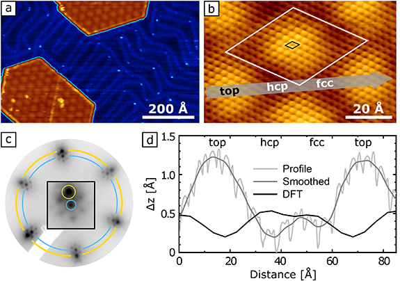
Figure 1. Geometric structure of MoS2/Au(111). (a) STM overview of MoS2/Au(111) (I = 440 pA,  mV). (b) Atomically resolved STM image (I = 460 pA, U = 50 mV), black diamond: MoS2 unit cell, white diamond: moiré unit cell. (c) LEED pattern (inverted contrast), E = 150.5 eV. Blue: MoS2, yellow: Au(111). (d) Profile along gray line in (b) from STM (raw data and smoothed) and DFT, see legend.
Download figure:
Standard image High-resolution imageFollowing previous studies, we identify the islands as MoS2 nanoflakes of one monolayer height [10–15, 18, 19, 21, 22]. The apparent height of the islands is small compared with the thickness of a single MoS2 layer as defined by the layer spacing in bulk MoS2 of 6.147 Å [23]. However, the apparent height determined by STM strongly depends on the electronic structure and can be very different from the geometric height, especially for a semiconducting material as MoS2. This can be illustrated by the strong dependence of the apparent height of MoS2 on tunneling voltage [18].
The atomically-resolved STM image in figure 1(b), shows the small scale periodicity of the MoS2 lattice and the superimposed long range periodicity of the moiré pattern where we label the different regions as top, hcp, and fcc, following [19]. The rationale of this nomenclature will be explained below. LEED (figure 1(c)) displays the characteristic moiré pattern consisting of first order spots of Au(111) and MoS2, surrounded by satellite spots in a hexagonal arrangement.
LEED indicates the precise alignment of the lattice vectors of MoS2 and Au(111). In consequence, also the lattice vectors of MoS2 and those of the moiré superstructure are strictly parallel. This is well visible the STM image in figure 1(b) where even a small misalignment would be well visible due to the amplifying effect of the moiré [24]. Our finding of rotationally aligned growth of MoS2 on Au(111) is in line with a recent study using spot profile analysis (SPA) LEED [13], a globally averaging technique with high resolution (HR) in reciprocal space.
Figure 1(d) shows the apparent height profile taken along the main diagonal of the moiré cell (gray arrow in figure 1(b)). We find a global maximum at the top and a local maximum at the bridge sites in between fcc and hcp. The peak to peak corrugation varies with tunnel conditions and tip, the largest value we found is ≈1 Å. For bias voltages close to zero the difference between the two minima is rather small. For high positive as well as large negative voltages  V, not shown) one minimum appears significantly higher, which allows us to identify this region as fcc [19].
We use the moiré pattern to determine the lattice parameters with high precision, and without errors caused by piezo creep, drift, STM calibration or distortion [24]. In the case of precise alignment of both lattices as found here, the moiré unit cell is formed by  MoS2 unit cells on
 ![$([m+1] \times [m+1])$](https://content.cld.iop.org/journals/2053-1583/9/2/025003/revision2/tdmac4958ieqn5.gif) Au(111) unit cells (
Au(111) unit cells ( Å [25]). We find
  (error is the standard deviation resulting from several measurements at different positions), leading to
  Å and
Å and  Å. The closest commensurate approximation of the moiré cell is
  MoS2 unit cells on
  Au(111) unit cells, or 11-on-12 for short.
Our lattice constant agrees within error bars with the bulk lattice constant of  Å [23]. The result for the periodicity of the moiré superstructure differs from recent findings. Bana et al find a 10-on-11 unit cell by SPA LEED [13]. The discrepancy may be due to difficulties in the calibration of electron diffraction patterns. Tumino et al find lattice constants of
  Å and
Å and  Å [18] determined via Fourier transformation of a large MoS2 area, and decided to use a 10-on-11 unit cell in DFT [22]. However, the 11-on-12 supercell is also within their limits of error. Our results have increased accuracy as we take advantage of the magnifying effect of the moiré.
We perform a DFT calculation (see section 4) for one  MoS2 layer on top of three (
 ) Au layers. The relaxed structure is shown in figure 2. Three regions of high symmetry (white circles) are evident that we label by the position of S in the lower layer with respect to Au(111), because this determines the local interaction. In the top region S is on top of a gold atom, whereas in the fcc-region (hcp-region) it resides in a threefold-hollow site of fcc (hcp) type. The latter two regions behave very similarly and are often summarized as hollow region. Figure 2(b) shows the side view cut along the main diagonal exposing the (1
 0) plane. The height of S in the upper layer along this cut is plotted in figure 1(c). It is obvious that the apparent corrugation in STM is inverted and has a larger amplitude. We will show in the following that the apparent height in STM is dominated by electronic effects, meaning that the maxima in the top region are caused by a high local density of states that overcompensates the small distance between MoS2 and Au(111) in these areas.

Figure 2. Relaxed structure of 2 H-MoS2/Au(111) obtained by DFT. (a) Top view. Spheres denote S (yellow), Mo (purple) and Au coded by layer (brown-green-blue). White diamond:  /
/ unit cell, regions of high symmetry are labeled. (b) Side view cut in the (1
 0) crystallographic plane (main diagonal in (a)). (c) Charge density difference in the same cut as in (b). The isosurface corresponds to 0.008 e
 with the charge accumulation (depletion) plotted in red (blue). This figure has been generated using VESTA [26].
Download figure:
Standard image High-resolution imageThe vertical distribution of the atoms is described in table 1. The minimum height of  Å of the S atoms in the lower layer (S1) is found for the top region. The Mo layer and the upper S layer (S2) follow the lower layer with very similar corrugation. The average thickness of the MoS2 monolayer (defined as the S-S distance) is 3.11 Å, which is slightly reduced with respect to bulk 2 H-MoS2 (3.19 Å [23]).
Table 1. Mean height  , minimum height hmin, maximum height hmax and corrugation
  of the atoms in the lower (S1) and upper (S2) sulfur layer as well as the Mo layer, referenced to the topmost Au layer. All values in Å.
| S1 | Mo | S2 | |
|---|---|---|---|

| 2.72 | 4.28 | 5.83 |
| hmin | 2.50 | 4.43 | 5.64 |
| hmax | 2.87 | 4.08 | 5.97 |

| 0.37 | 0.35 | 0.33 |
The charge density difference in the central (1 0) plane is shown in figure 2(c). The regions are markedly different: In the top region charge accumulates between S and Au, indicating a chemical bond (chemisorption). The charge stems from the pz
atomic-like orbitals of the S atoms and the d-orbitals of the Au atoms underneath. There is much less charge transfer in the hollow regions. Moreover, the charge accumulation at the hybrid MoS2-Au(111) interface goes along with a site-dependent charge rearrangement between the interfacial S atoms and the Mo atoms. This rearrangement modulates the strength of S-Mo chemical bond in the MoS2 layer.
0) plane is shown in figure 2(c). The regions are markedly different: In the top region charge accumulates between S and Au, indicating a chemical bond (chemisorption). The charge stems from the pz
atomic-like orbitals of the S atoms and the d-orbitals of the Au atoms underneath. There is much less charge transfer in the hollow regions. Moreover, the charge accumulation at the hybrid MoS2-Au(111) interface goes along with a site-dependent charge rearrangement between the interfacial S atoms and the Mo atoms. This rearrangement modulates the strength of S-Mo chemical bond in the MoS2 layer.
In order to scrutinize the DFT calculation we applied the method of XSW (see section 4 for experimental details). We prepared samples using virtually identical parameters except an increased number of growth cycles leading to a higher coverage (see section 4). The LEED pattern (inset of figure 3(a)) is qualitatively equivalent to the one shown in figure 1(c). The higher coverage of MoS2 is reflected in the increase of the intensity ratio between MoS2- and Au-related spots and the increased sharpness of the moiré satellites.

Figure 3. HR-XPS of MoS2/Au(111). (a) Mo 3d and S 2s (inset: LEED pattern, inverted contrast, E = 75.5 eV), (b) S 2p. XPS of (c) Mo 3d and S 2s, (d) S 2p. Circles: data points after background subtraction. Colored areas: fits of the indicated peaks and components (MoA 3d: dark cyan, MoB 3d: light cyan, S 2s: yellow, SA 2p: yellow, SB 2p: light yellow, SC 2p: orange). Solid black line: sum of fits.
Download figure:
Standard image High-resolution imageThe number of cycles is still low enough to avoid the growth of bilayers [12]. The absence of bilayers is also indicated by the LEED pattern: a significant coverage with bilayers should lead to a decrease of the moiré satellite spots, as in STM it is found that the moiré superstructure is not present on bilayers [12]. In our experiments, we find the opposite behavior.
Figure 3 shows HR-XPS of the core levels Mo 3d and S 2s (figure 3(a)), as well as S 2p (figure 3(b)). The fitting parameters of the main components are given in table 2. For S 2p we also find a minority component SC 2 p (
( eV,
eV,  eV). As demanded for XSW experiments, a higher incident photon energy of 2.63 keV (off-Bragg condition) has been used for the spectra depicted in figures 3(c) and (d), which changes the photoelectron cross sections and reduces resolution and surface sensitivity (partly compensated by detecting photoelectrons under a more grazing emission angle.) We observe an additional doublet MoB 3d at a lower binding energy of 228 eV (light blue in figure 3(c)).
Table 2. Key parameters of the components observed in photoemission (HR-XPS, XPS, and XSW). Binding energy EB, full width at half maximum Γ, mixing parameter for Voigt-like function β, spin-orbit-splitting  , intensity relative to the most intense component for soft (Isoft) and hard (Ihard) x-rays. Coherent position PH
(
, intensity relative to the most intense component for soft (Isoft) and hard (Ihard) x-rays. Coherent position PH
( ) and coherent fraction fH
(
) and coherent fraction fH
( ).
).
| HR-XPS | XPS | XSW | ||||||
|---|---|---|---|---|---|---|---|---|
| Component | EB (eV) | Γ (eV) | β |
 (eV) (eV) | Isoft | Ihard | PH | fH |
Mo 3d
| 229.19 | 0.26 | 1.00 | 3.14 | 1 | 1 | 0.81 | 0.90 |
| S 2s | 226.41 | 2.00 | 0.55 | — | 1 | 1 | 0.35 | 0.39 |
SA 2p
| 162.16 | 0.25 | 0.85 | 1.18 | 1 | 1 | 0.42 | 0.50 |
SB 2p
| 162.46 | 0.51 | 0.75 | 1.18 | 0.20 | 0.25 | 0.07 | 0.89 |
Our highly-resolved spectra are very similar to those presented by Bana et al [13], and the fitting parameters are almost identical. This also implies that in both studies the same phase, namely 2 H, is present. We observe two additional minor components (MoB 3d and SC 2p) which could be due to differences in the growth procedure. We tentatively attribute SC 2p to S atoms at the edges of MoS2 islands with reduced coordination [15]. MoB is assigned to metallic Mo on or embedded in Au(111) which was found at the very same binding energy in previous studies [15].
We performed an XSW analysis to determine the distribution of Mo and S perpendicular to the surface. In short, such an analysis yields two structural parameters: the coherent position  and the coherent fraction
  [27]. PH
is the average height of all atoms of the analyzed species and fH
indicates the distribution of atoms around this mean height (
[27]. PH
is the average height of all atoms of the analyzed species and fH
indicates the distribution of atoms around this mean height ( for a δ-like distribution). The average height of a species is given by
  , where
  Å [25] is the Bragg plane spacing of Au(111). The dependence of the photoelectron yield on the x-ray energy for the main Mo 3d
 peak, the S 2s peak, and the two most intense S 2p
 peaks is presented in figure 4. The resulting structural parameters coherent position PH
and coherent fraction fH
are given in table 2. However, only for Mo a direct interpretation of these parameters is possible:
peaks is presented in figure 4. The resulting structural parameters coherent position PH
and coherent fraction fH
are given in table 2. However, only for Mo a direct interpretation of these parameters is possible:  yields a mean Mo height of (
 ) Å above the virtual unrelaxed surface,
  indicates a very flat layer. The S components are a convolution of different species, and thus an interpretation is only possible by comparison to the DFT calculation.

Figure 4. XSW results for MoS2/Au(111). The analysis is presented for each component (MoA 3d , S 2s , SA 2p
 and SB 2p
 ) showing the variation in total photoelectron yield as function of the photon energy scan along the reflectivity curve. The values of coherent position (PH
) and coherent fraction (fH
) are shown to each component analysis.
) showing the variation in total photoelectron yield as function of the photon energy scan along the reflectivity curve. The values of coherent position (PH
) and coherent fraction (fH
) are shown to each component analysis.
Download figure:
Standard image High-resolution imageTable 3 compares PH and fH derived from the DFT-calculated atomic positions (see section 4) with the experiment. For Mo the assignment of the atoms to an atomic species is simple and we obtain a good agreement between theory and experiment, especially for the more robust parameter coherent position: whereas fH is diminished by thermal disorder as well as by any contamination (adatom, incorporated in bulk, island edges, grain boundaries), such presumably broadly distributed atoms have a negligible effect on PH .
Table 3. Comparison between the structural parameters determined by XSW for each component and by a model for the assigned species based on DFT. The model is based on an attenuation factor of α = 0.76 and a strongly bound fraction of the lower S layer of f = 0.45, see text. Experimental values are indicated in bold.
| Component | Mo 3d
| S 2s | SA 2p
| SB 2p
| |
|---|---|---|---|---|---|
| Species | Mo | S1 S1 S1 S2 S2 | S1 S2 S2 | S1t | |
| PH | Experiment | 0.81 | 0.35 | 0.42 | 0.07 |
| Model | 0.82 | 0.35 | 0.41 | 0.12 | |
| fH | Experiment | 0.90 | 0.39 | 0.50 | 0.89 |
| Model | 0.97 | 0.53 | 0.66 | 0.98 |
For sulfur, the comparison is not as simple. First, there are different species of S in MoS2/Au(111), and second, not all photoelectrons from the lower S layer reach the detector due to attenuation by the Mo layer and the upper S layer. We propose a model (guided by DFT) where we distinguish three different species of S: all sulfur atoms in the upper layer belong to one species (S2), but for the lower layer we distinguish two species: a fraction of  belongs to S1h that are sulfur atoms weakly bound to the gold substrate (S-hollow), and a fraction of f belong to a strongly bound species S1t (S-top). We describe the attenuation with a parameter α defined as the fraction of photoelectrons from the lower S layer reaching the detector as compared with the upper one.
We start with the core level S 2s (top-right in figure 4). As the corresponding photoemission peak shows just one component, all sulfur atoms must contribute (S1 S1
S1 S2). The calculated structural parameters, corresponding to all S atoms present in the DFT model, are
  and
and  , clearly deviating from experiment (see table 2). This discrepancy can be solved by taking into account that the weight of the lower S layer is reduced by α due to attenuation. The best description of our experimental data is found using α = 0.76.
With α = 0.76 it is clear that the XPS component SB 2p cannot be due to the full lower layer, because in this case its relative intensity should just be
  , in clear contrast to the experimental value
  . Under the assumption that only strongly bound atoms of the lower layer (S
 , fraction f) contribute to the component SB, while all other S atoms contribute to SA, we find
  , yielding f = 0.45. In other words, roughly half of the lower S qualify as strongly bond, the other half as weakly bound. Thus one can calculate the structural parameters PH
and fH
corresponding to 45% of S atoms closest to the Au surface as the best model for the component SB 2p
, yielding f = 0.45. In other words, roughly half of the lower S qualify as strongly bond, the other half as weakly bound. Thus one can calculate the structural parameters PH
and fH
corresponding to 45% of S atoms closest to the Au surface as the best model for the component SB 2p , leading to satisfactory agreement (see table 3).
The remaining S atoms contribute to the component SA 2p . Here, both parameters α and f enter in the respective weight of the atoms used to determine PH
and fH
. The good agreement, especially for the coherent position, verifies our approach. Another piece of evidence for our model is the very low coherent fraction of
. Here, both parameters α and f enter in the respective weight of the atoms used to determine PH
and fH
. The good agreement, especially for the coherent position, verifies our approach. Another piece of evidence for our model is the very low coherent fraction of  , which cannot be explained in a model that attributes this component to the top layer alone (DFT prediction
  ).
).
The comparison between the experimental results and the model based on DFT calculations is summarized in an Argand diagram (figure 5). The good agreement validates the DFT calculation and our advanced model. In a complex system as found here, where the same chemical species is present in different layers, an interpretation of the XSW data is only possible by a comparison to a dedicated model as performed here. The failure of a straightforward interpretation of SA 2p as the upper S1 layer and SB 2p
 as the lower S2 layer is directly visible in the Argand diagram: in this case, the symmetry of MoS2 demands that MoA 3d
 forms the bisector of the two S components, which is clearly not found in experiments.
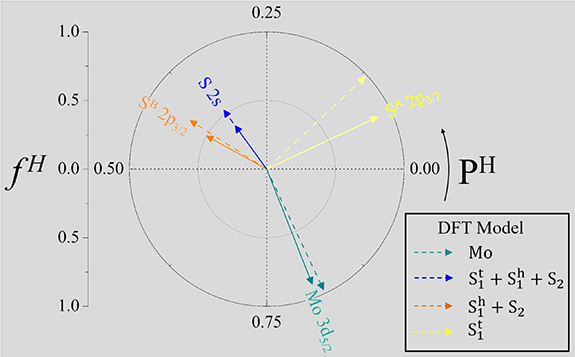
Figure 5. Argand diagram: a vectorial representation combines the coherent positions PH (polar angle) and coherent fractions fH (vector length). Solid vectors: XSW results (see labels), dashed vectors: model based on DFT (see legend).
Download figure:
Standard image High-resolution imageTo reiterate: we observe two main sulfur species in MoS2 on Au(111). However, the straightforward interpretation that one belongs to the sulfur atoms in close contact with the substrate in the Au-S-Mo-S sequence, and the other one belongs to sulfur atoms at the vacuum side, does not agree with our experimental findings. Instead, we have to distinguish between sulfur atoms in the lower layer that can form a comparatively strong bond to Au atoms due to a favorable on-top-registry (significant chemical shift), and all other sulfur atoms, both in the lower and the upper layer (no chemical shift).
Our assignment of the components forming the S 2p peak differs from the one presented in [13]. Whereas in this paper the two peaks are ascribed to the sulfur in the different layers, our data indicates that the distinction is between S strongly bound to Au(111) and nearly undisturbed sulfur atoms from both layers. As the component SB 2p
 stems exclusively from the lower layer, and the XPS signal from the component SA 2p
 is dominated by the upper layer, the conclusions drawn from the x-ray photoelectron diffraction (XPD) in [13] may still remain valid.
Comparison of the XP spectra of MoS2/Au(111) with those of the closely related material TaS2/Au(111) measures under very similar conditions [28] reveals qualitative differences: in both systems, two main components for the S 2p level are present, but the intensity ratio is much closer to one for TaS2, where each component could be assigned to a specific S layer. This further supports our model that for MoS2 the less intense component stems only from a fraction of the S atoms in the lower layer. We speculate that the reason for the different behavior of TaS2 is its metallic nature that smooths out strong variations in electron density.
In comparison to other epitaxial 2D materials, the MoS2 layer on Au(111) is rather flat, even though the chemical difference (as evidenced by XPS) between the strongly and weakly bound region is quite pronounced. The strong corrugation observed in STM (up to 1 Å) is completely due to electronic effects, evidencing the difficulty of a precise determination of the vertical structure using scanning probe methods.
2.2. Electronic structure
We use STS to investigate the electronic properties of MoS2/Au(111) (see section 4). Figure 6(b) shows the spectra in the normalized form ![$[({\textrm{d}} I/ {\textrm{d}} V)/(I/V)]$](https://content.cld.iop.org/journals/2053-1583/9/2/025003/revision2/tdmac4958ieqn79.gif) , where artifacts of voltage and tip-sample separation are reduced [29]. We observe three prominent peaks, one for the occupied states (O1) and two for the empty states (E1, E2). The positions of the peaks depend on the moiré region, see table 4. The peak positions for the fcc and hcp region are very similar, whereas the peaks in the top region are shifted towards lower energies, especially O1.
, where artifacts of voltage and tip-sample separation are reduced [29]. We observe three prominent peaks, one for the occupied states (O1) and two for the empty states (E1, E2). The positions of the peaks depend on the moiré region, see table 4. The peak positions for the fcc and hcp region are very similar, whereas the peaks in the top region are shifted towards lower energies, especially O1.

Figure 6. Moiré dependence of the electronic states. (a) Color plot of a line scan over a full moiré unit cell and (b) normalized d dV spectra recorded at the high symmetry regions of the moiré pattern. The tip was stabilized at
  eV and I = 310 pA (line scan), I = 510 pA (single spectra). (c) Total DOS, summing up the pDOS of s,p,d orbitals. (d) STM and STS maps of MoS2/Au(111) at different energies. I = 510 pA, image size 8 Å × 8 Å.
Download figure:
Standard image High-resolution image
Table 4. Energies of the peaks observed by STS (in eV) for each moiré region. The error, determined by the energy resolution of the STS measurement, is 0.02 eV.
| Peak | Top | Fcc | Hcp |
|---|---|---|---|
| O1 | −2.02 | −1.80 | −1.75 |
| E1 | 0.90 | 0.92 | 0.93 |
| E2 | 1.40 | 1.44 | 1.46 |
Our normalized d dV spectra are virtually identical to the ones measured in [19], where also O1 (named Q in [19]), E1 (Γ1), and E2 (Γ2) are observed. The spectra found in [21] are different. In these studies, the sample was exposed to air between preparation and measurement, which is not the case for our experiments as well as for [19]. By comparing our peak energies with ARPES [14] and the band structure resulting from DFT calculations in a simplified model [21], we assign O1 to the VB minimum at Γ, which ARPES finds at
  eV. Similarly, we ascribe E2 to the CB minimum at Γ. The assignment for E1 is somewhat more difficult. We find local CB minima at matching energies near M as well as between Γ and Q. Presumably, all these states contribute to E1. However, since the states between Γ and Q have smaller parallel momentum
  , they will dominate the tunneling signal and thus we primarily associate E1 with these states (which are found at significantly higher energy than for freestanding MoS2).
There is agreement as well as disagreement with the assignment of the peaks by Krane et al [19]. The authors based their interpretation on measurements of the decay constant of the tunnel current κ, which contains information on  [30]. They find a low value of κ for E2 and higher and mutually similar values for E1 and O1. Consequently, they assign E2 to the minimum of the CB at Γ and O1 to the VB minimum at Q. They do not attribute E1 to a specific state. We follow the assignment for E2, but disagree for O1. The energy of the valence band minimum at Q is determined by ARPES as
  eV [14], which is considerably higher than the energy observed by STS. A much better match is found for the band maximum around Γ at
  eV, which appears very broad and diffuse in ARPES. DFT calculations show that the maximum of a singular band observed for free-standing MoS2 is destroyed by hybridization with Au(111). Instead new band extrema in the vicinity of Γ appear (approximately halfway between Γ and Q, see figure 5 of [21]), which can explain the value of κ . Therefore, we assign O1 to these new hybridization states near Γ.
We map the electronic structure across one moiré unit cell by taking d dV spectra at several points along the main diagonal of the moiré cell (see gray line in figure 1(b)) and display them as a color plot (figure 6(a)). The positions of the peaks shift within the moiré structure, especially for O1. In agreement with the point spectra, we observe maxima at the fcc and hcp positions and minima at the top position. Furthermore, we find additional minima at the bridge position, which is at a similar energy as for the top position.
Figure 6(c) shows the DOS calculated by DFT for top and fcc/hcp hollow moiré regions. Two prominent peaks for the empty states, which correlate to E1 and E2, are visible. The peak with the highest intensity in the occupied states can be associated with O1. There are additional peaks, particularly for the conduction and valence band onsets at K, that are not or only faintly visible in  spectra. Furthermore, the DOS of the top area is shifted compared to the DOS of the hollow sites, in the same direction as in experiment.
In agreement with experiment, the shift is largest for O1 and smallest for E1. The shift is significantly larger than the experimentally observed shift, especially for E1 and E2, but not rigid. This discrepancy may be caused by including the vdW interaction in our DFT calculations as a correction term, which improves the structural results, but does not act on the electronic properties.
The energy of O1 is strongly modulated by the moiré structure as already indicated in [19]. We attribute this modulation to the varying degree of hybridization between this state and states of the substrate. The overlap of the corresponding orbitals is not a simple function of the S-Au distance as the energy of O1 at the bridge position is similar to the one at the top position, even though the local MoS2 height is very different (see figure 1(c)). The interaction is rather determined by the relative position of the lowest S atoms towards the surface Au atoms and the involved orbitals (S pz
and Au d ): if the dense packed S atomic rows are in phase with the dense packed rows of the Au surface (top and bridge regions), the interaction is strongest. In the fcc and hcp moiré areas the S pz
-orbitals point into the fcc and hcp gaps of the Au surface. Correspondingly, the impact is strongest for O1, since the VB edge at Γ is foremost of out-of-plane (S pz
, Mo 4d
): if the dense packed S atomic rows are in phase with the dense packed rows of the Au surface (top and bridge regions), the interaction is strongest. In the fcc and hcp moiré areas the S pz
-orbitals point into the fcc and hcp gaps of the Au surface. Correspondingly, the impact is strongest for O1, since the VB edge at Γ is foremost of out-of-plane (S pz
, Mo 4d ) orbital character [21, 31]. In contrast, the CB at Γ (E2) mostly originates from in-plane (S px
, py
) orbitals, thus interacting less strongly with the substrate (or their interaction depends less strongly on the local registry) and stays at nearly constant energy.
) orbital character [21, 31]. In contrast, the CB at Γ (E2) mostly originates from in-plane (S px
, py
) orbitals, thus interacting less strongly with the substrate (or their interaction depends less strongly on the local registry) and stays at nearly constant energy.
In addition to  point spectra we map the electronic effects of the moiré potential at different energies (figure 6(d)). While there are certainly subtle changes in the STM images (as discussed in [19]), more significant differences are found in the STS maps. The relative intensity of the top, hcp and fcc regions strongly depends on the bias voltage. Most obvious are four contrast inversions between top and hollow moiré sites: between −2 eV and −1.5 eV the contrast changes from bright top and dark hollow to dark top and bright hollow areas. The next contrast inversion happens between −0.5 eV and 0.5 eV in reversed order. At 1.5 eV the top areas again appear dark surrounded by a network of bright hollow regions. The contrast changes back to bright top and dark hollow regions at 2.5 eV. The contrast inversions are accompanied by slight changes in the intensity distribution of fcc and hcp sites. At 1 and 2 eV all intensity is focused on fcc (downward pointing triangles) and hcp sites (upward pointing triangles), respectively.
The contrast inversion between −2 and −1.5 eV reflects the shift of O1. The nuanced changes at positive bias voltages reveal a more complex influence of the moiré pattern to the conduction band states, in agreement with subtle changes found in constant current  spectra by Krane et al [19].
The apparent height profile of the moiré corrugation measured with STM and the height profile calculated with DFT are exactly inverted. Whereas STM finds a strong corrugation with high top and low hollow regions, DFT predict a very low corrugation with low top and high hollow regions, in agreement with XSW results. Spatially depended STS measurements reveal that the moiré corrugation observed in STM is a pure electronic effect and we attribute the moiré modulation to the varying degree of hybridization between states of the bottom S atoms and substrate states.
The spatial variation of O1 also explains the diffuse appearance of the VB maximum at Γ in ARPES [14]. Our  spectra exhibit a well defined peak for O1, showing that locally the state is well-defined. The key effect behind the broadening is the moiré dependent modulation of the substrate interaction. Since the ARPES signal is averaged over several moiré unit cells, these local variation of the VB maximum can not be resolved.
An alternative explanation of the peak shifts could be based on screening of MoS2 states by the highly polarizable metal substrate [16, 17], which becomes stronger with decreasing height of the MoS2. Screening is expected to move states towards the Fermi level. However, for O1 we observe the opposite behavior as it moves away from EF when we go from the weakly to the strongly bonded regions. This implies that screening effects are not significant in our system.
3. Conclusion
In conclusion, our moiré analysis yields highly precise values for the lattice constant of MoS2/Au(111), indicating that 11-on-12 is the best commensurate approximation. We perform DFT calculations using a realistically large unit cell and including non-local interactions that are substantiated by a good match with XSW measurements. Thereby, we can show that the apparent corrugation observed in STM is inverted with respect to the actual height of the atoms. In addition, the 2D layer is very flat, in contrast to its appearance in STM. DFT calculation reveals that hybridization between S orbitals and states of the substrates is the main contribution to the bonding. As this hybridization shows a spatial variation across the unit cell, specific regions of the MoS2 (top regions) are strongly bonded, whereas others (hollow regions) interact only weakly. This leads to the occurrence of different components for S atoms in photoelectron spectra that we could unambiguously attribute to specific species of S. Our STS measurement revealed pronounced changes of the electronic structure across the unit cell that are caused by the variation in hybridization rather than by screening. We could assign all observed peaks to specific electronic states of MoS2.
4. Methods
We used ultra-high vacuum systems located in Köln, Germany (Createc Fischer, base pressure  mbar) for STM/STS, and at Diamond Light Source, UK (DLS, [32],
  mbar) for XPS/XSW.
Prior to growth, clean Au(111) was prepared by 1.5 keV Ar+ sputtering and annealing to 973 K (Köln) (873 K (DLS)). Cleanliness was verified by LEED. MoS2 was prepared in situ following the procedure described in [11] and [12]: Mo was evaporated with a rate of ≈ 0.05 Å min−1 (calibrated with a quartz crystal microbalance) for 5 min using an e-beam evaporator (SPECS EBE-4 (OAR EGN4)) with the sample at room temperature. In parallel, the sample was exposed to H2S using a tube of 12 mm diameter ending 20 mm in front of the sample, resulting in a background pressure of  mbar. After the evaporation is stopped, the sample is annealed for 30 min at 853 K (843 K) while the exposure to H2S is continued. The exposure was stopped directly (5 min) after the heating. A full preparation consisted of one (four) of such cycles.
Electron diffraction patterns were obtained by an MCP LEED (K) and a standard LEED optics (DLS). Images recorded with the MCP LEED need to be corrected for distortions caused by the planar arrangement of the microchannel plates. Correction is done with the program MCPdeskew [33], details of the correction procedure and the required geometric parameters are found in [34].
STM and STS measurements are carried out at 5 K in a chamber separated from the growth chamber (sample transfer under UHV) with a background pressure lower than 10−11 mbar. The d dV point spectra and constant energy maps are recorded using the lock-in technique (modulation frequency 777.3 Hz, time constant 30 ms). The modulation amplitude was 10 mV, providing an energy resolution of 20 meV [35]. An etched tungsten tip is used for all measurements, which is prepared in situ by dipping the tip into the gold substrate and measuring the Au(111) surface state [36] to ensure the sensitivity to the LDOS. STM images and STS maps are analyzed with the SPIP software [37].
The XPS and XSW experiments were performed in the end-station of the I09 beamline at DLS (sample transfer under UHV). To combine different techniques, the beamline was designed to provide both soft (100–2100 eV) and hard (2.1–20 keV) x-rays, which are directed to the same spot on the sample. The end-station is equipped with a hemispherical electron analyzer (VG Scienta EW400 HAXPES) with a 17 frame/s CCD camera, having an angular acceptance of 56∘. The HR-XPS data were acquired at an emission angle  and a photon energy of
  eV. For the fitting of HR-XPS data, a Shirley-type background [38] was subtracted and the core-level peaks were adjusted by a sum of Voigt-like functions characterized by a mixing parameter β (β = 1 for pure Lorentzian) as described in our previous work [39]. For Mo 3d
 and Mo 3d
 the mixing parameter was 1 indicating a pure Lorentzian function. The values of spin–orbit splitting were initially constrained to 3.15 and 1.20 eV for Mo 3d and S 2p, respectively. The values shown in table 2 are the optimized values after the fitting process. Errors in the binding energy determination were estimated as
  eV.
eV.
The XSW measurements were performed in backscattering geometry using the (111) Bragg reflection of Au(111). Photoelectrons from core levels Mo 3d, 2s and S 2p were acquired during the scan of the photon energy around the Bragg energy  keV with
  . This configuration allows us to treat the non-dipolar contributions from the photoelectron yield in the same manner as in our prior work [40]. The model applied to the photoemission spectra obtained during the XSW experiment was based on the fitting of HR-XPS data. Thus, the difference in binding energy between the peak components was constrained to the values found in HR-XPS. Furthermore, during the XSW analysis, the width of peak components were constrained in order to avoid changes in the components' intensities other than those caused by the standing wave effect. The analysis of the dependence of the photoelectron yield on incident photon energy, described by the dynamical theory of x-ray diffraction, results in the structural parameters PH
(coherent position) and fH
(coherent position) [27, 41]. PH
is the Fourier-averaged position of all atoms of the analyzed species relative to the lattice planes of the substrate and fH
describes the distribution of atoms around the position given by PH
. The distance between the center of the height distribution for all analyzed atoms and the substrate lattice plane is given by
. This configuration allows us to treat the non-dipolar contributions from the photoelectron yield in the same manner as in our prior work [40]. The model applied to the photoemission spectra obtained during the XSW experiment was based on the fitting of HR-XPS data. Thus, the difference in binding energy between the peak components was constrained to the values found in HR-XPS. Furthermore, during the XSW analysis, the width of peak components were constrained in order to avoid changes in the components' intensities other than those caused by the standing wave effect. The analysis of the dependence of the photoelectron yield on incident photon energy, described by the dynamical theory of x-ray diffraction, results in the structural parameters PH
(coherent position) and fH
(coherent position) [27, 41]. PH
is the Fourier-averaged position of all atoms of the analyzed species relative to the lattice planes of the substrate and fH
describes the distribution of atoms around the position given by PH
. The distance between the center of the height distribution for all analyzed atoms and the substrate lattice plane is given by  , where
  Å [25] is the Au(111) Bragg plane spacing. The errors of XSW measurements are determined following Mercurio et al [42].
Our DFT [43, 44] calculations have been carried out using pseudopotentials generated with the projector augmented wave method (PAW) [45] as implemented in the VASP code [46–48]. The moiré structure of MoS2/Au(111) was modeled by a slab made of three Au atomic layers with an (11×11) MoS2/(12×12) Au(111) in-plane unit cell amounting to a total of 795 atoms. With the Brillouin zone sampled by the Γ-point and a cutoff energy of 500 eV, the ground-state geometry of this moiré cell was obtained by relaxing the atomic degrees of freedom of the MoS2 and the first Au surface layer with a threshold value of the calculated forces of 20 meV  . Furthermore, the non-local correlations effects responsible for the van der Waals (vdW) interactions acting between MoS2 and Au(111) were described with the help of the vdW-DF2 functional [49] together with the exchange energy functional proposed by Hamada [50].
The structural parameters PH and fH connected to the DFT model were calculated by using the atomic coordinates resulting from the optimized relaxation in the equations (3.6)–(3.13) of [27].
Acknowledgments
The authors gratefully acknowledge the Gauss Centre for Supercomputing (GCS) for providing computing time through the John von Neumann Institute for Computing (NIC) on the GCS share of the supercomputer JURECA at Jülich Supercomputing Centre (JSC). V C, S B and N A gratefully acknowledge financial support from the Deutsche Forschungsgemeinschaft (DFG) through the Collaborative Research Center SFB 1238 (Project No. C01). We acknowledge Diamond Light Source for the award of beam times (SI14799-1, SI16710-1, and SI19801-1). P T P R was supported by the Advanced Characterisation of Materials (ACM) CDT. We acknowledge fruitful discussions with M. Rohlfing (Münster).
Data availability statement
The data that support the findings of this study are available upon reasonable request from the authors.