
Abstract
Present work investigates the structural, electronic and magnetic properties of Gd doped wurtzite GaN nanowires (NWs) oriented along the [0001] direction in presence of intrinsic defects by employing the GGA + U approximation. We find that Ga vacancy (VGa) exhibits lower formation energy compared to N vacancy. Further stabilization of point defects occurs due to the presence of Gd. The strength of ferromagnetism (FM) increases by additional positive charge induced by the VGa. Electronic structure analysis shows that VGa introduces defect levels in the band gap leading to ferromagnetic coupling due to the hybridization of the p states of the Ga and N atoms with the Gd d and f states. Ferromagnetic exchange coupling energy of 76.4 meV is obtained in presence of Gd-VGa complex; hence, the FM is largely determined by the cation vacancy-rare earth complex defects in GaN NWs.
Export citation and abstract BibTeX RIS

Content from this work may be used under the terms of the Creative Commons Attribution 3.0 licence. Any further distribution of this work must maintain attribution to the author(s) and the title of the work, journal citation and DOI.
1. Introduction
Gallium Nitride (GaN) nanowires (NWs) have several promising electronic and optoelectronic applications, ranging from light emitting diodes to sensing devices, high power transistors to spintronics, due to its wide direct band gap and structural confinement properties [1–5]. Owing to the recent advancements in experimental techniques, it has been possible to successfully synthesize and characterize GaN NWs [1–3, 6]. In general, semiconductor NWs possess superior mechanical quality at high temperatures compared to bulk, rendering them more desirable candidates for spintronic devices [7]. It is well established that NW properties can be modified by changing the concentration of native defects, as well as by the introduction of external impurities [8–11]. The most common dopants in GaN NWs include transition metals (TMs) and rare earth (RE) elements. The structural, magnetic and optical characteristics of TM- [12, 13] and RE-doped GaN NWs [14–16] are currently being investigated using a wide range of experimental techniques. The cylindrical geometry and large surface to volume ratio characterizing the NWs can enhance the spin polarization significantly, while reducing the formation energy (Ef) of impurities [8, 17]. In addition, RE-doped GaN has been the subject of intensive research focusing on bulk materials [18–24]. However, the magnetic properties of the RE-doped GaN NWs observed experimentally, is still not well understood and the previous theoretical studies tend to focus solely on the effects of native defects and TM dopants [10, 11, 17, 25–27]. Thus, further theoretical studies can advance the understanding of the role of impurities and defects in explaining the experimental findings of GaN NWs. In this scenario, RE-doped GaN NWs present an interesting research problem from the fundamental and technological point of view. In particular, Gd is one of the promising RE dopants, reported to carry high magnetic moments and enhanced Curie temperatures in bulk GaN [18, 23, 24]. However, the mechanism of the magnetic and electronic behaviors of Gd-doped GaN NW has not been investigated thus far.
The NW diameters can be tuned from 1 nm to as large as 200 nm; the former possess distinct magnetic, optical and transport properties, compared to larger diameter NWs due to quantum confinement effects [7, 9, 28]. Owing to computational limitations, theoretical studies are often restricted to the modeling of NWs of few nm in diameter. However, recent advances in fabrication techniques have enabled synthesizing NWs of small diameters (1.5 to 5 nm) [28, 29]. Therefore, density functional theory (DFT) studies have been successful in predicting comparable results [30]. Moreover, DFT investigations on small-diameter nanowires assists in understanding the quantum confinement effects that give rise to significant density of states (DOS) near the band edge [31]. In this work, we show that Gd-doped GaN NWs have a potential for practical applications in spintronic devices operating at room temperature (RT). We report a systematic study, incorporating both native defects and Gd dopants in GaN NWs. A GaN NW of 1 nm diameter is considered, which is adequate for investigating the relative stability and clustering effects of Gd in the dilute limit.
2. Methodology
The present study investigates a wurtzite Ga48N48 NW along the [0001] direction modeled using the supercell approach. The length of the supercell is 2c, where c is the bulk lattice parameter along the [0001] direction, such that the simulation cell contains 4 GaN atomic layers with 96 atoms. For the planes perpendicular to the growth direction, vacuum region of ∼20 Å is used to ensure negligible interaction between the periodically repeated NW images. On the other hand, along the z-direction, infinite periodicity is maintained. The computations are performed using the Vienna Abinitio Simulation Package (VASP) [32, 33]. A cut-off energy of 400 eV is used to expand the plane waves contained in the basis set. The pseudopotentials used are that of projected augmented wave basis [34] with GGA in the Perdew Burke–Ernzerhof form for exchange and correlations [34]. Atomic coordinates are relaxed within energy and force tolerances of 0.0001 eV and 0.004 eV Å−1, respectively. The Brillouin zone is sampled using a (1 × 1 × 2) Monkhorst pack k-grid for the total energy calculations, whereas a larger k-grid of (1 × 1 × 8) is used for the electronic structure analysis. We employ the GGA + U method for our calculations, as it is well known that standard DFT may not accurately describe the electronic structure of GaN due to strong electronic correlations of the 3d electrons. The parameters used in the calculations comprise on-site Coulomb parameter U = 6.7 eV with a J value of 0.7 eV for Ga, and U = 7.4 eV with a J value of 0.5 eV for Gd, in line with the Duradev's approach [35], as implemented in VASP.
3. Results and discussion
Initially, the bulk unit cell parameters for wurtzite GaN is calculated for the purpose of comparison with experimental results. The obtained lattice parameters a = 3.18 Å and c = 5.19 Å are in good agreement with the experimental values (a = 3.1876 Å; c = 5.1846 Å) [36], establishing the accuracy of our calculations. These optimized lattice parameters are used to construct the GaN NW, which is subjected to further optimization. Obtaining stable structure for the NW is important due to the large surface area to volume ratio of nanostructures. After the relaxation, the Ga-N bond length suffers distortion along the c-direction, and decreases to 1.85 Å compared to that in bulk GaN (1.95 Å) [36]. The Ga-N bond length of the surface atoms is ∼1.87 Å in the a–b plane, while that of the inner atoms is ∼1.92 Å. As expected, the surface atoms are characterized by shorter average bond lengths than the inner atoms, due to the reduced coordination numbers. In bulk GaN, the distance between the second nearest neighbor Ga atoms is 3.21 Å, while it is reduced to ∼2.97 Å in the NW. The decrease in the bond length obtained in NWs is a result of the increased surface to volume ratio, and similar trends have been reported in previous first principles studies [10, 37]. We compare the total densities of states (TDOS) of bulk GaN and pristine GaN NW calculated using the GGA + U approximation as shown in figure 1. The position of Fermi level (EF) is almost identical for both bulk and NW structures, revealing the semiconducting characteristics of the NW, because Gd3+ ions located at the Ga sites are an isovalent impurity in GaN. The DOS of pristine NW shows zero spin-polarization, exhibiting a non-magnetic nature similar to the bulk GaN.
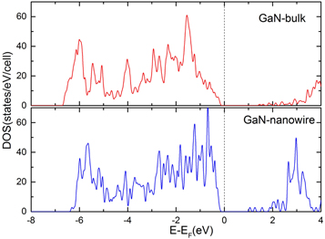
Figure 1. The total DOS corresponding to bulk GaN and pristine Ga48N48 NW.
Download figure:
Standard image High-resolution imageTo analyze the possibility of dopant-induced magnetism, one Gd atom is incorporated into the Ga site in the GaN NW. This approach is in accordance with experimental findings, as RE dopants preferentially occupy Ga sites in GaN [38]. The calculations are performed for 12 non-equivalent configurations, grouped into three categories to encompass the bulk-like, subsurface and surface positions, to investigate the more stable location of Gd atoms in NWs, as shown in figure 2. Relaxation without spin or geometrical constraints is carried out to identify the most stable configuration. The Ef of these NW configurations are calculated according to [8]

where Ed(total) and E(Ga48N48) denote the total energy of the NW containing Gd and total energy of the pristine GaN NW, respectively; ni represents number of atoms removed/added for respective elements; μi is the chemical potential, which is the total energy calculated for metallic Ga and Gd elements.

Figure 2. The GaN NW with Gd doping. The twelve non-equivalent doping sites are grouped into three and each location is numbered as indicated in the figure. The Ga and N atoms are indicated by pink and dark yellow colors, respectively. The three non-equivalent Gd sites are represented by bright yellow, blue and silver colors respectively.
Download figure:
Standard image High-resolution image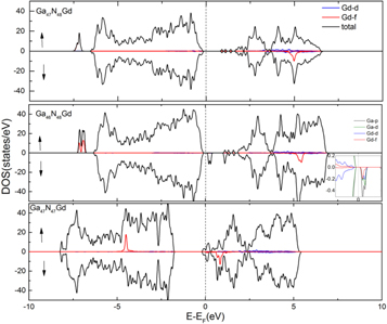
Figure 3. The TDOS of Gd doped GaN NW (Ga47N48Gd), Gd doped NW with VGa (Ga46N48Gd) and with VN (Ga47N47Gd), along with projected DOS of Gd d and f orbitals. The inset in the middle panel shows the projected DOS of Ga and Gd atoms in Ga46N48Gd NW.
Download figure:
Standard image High-resolution imageThe Ef calculated for each configuration is presented in table 1, which shows that the most stable Gd location is obtained at the surface of the NW. This implies the effect of self-purification observed in nanomaterials. When the impurities and defects require high energy to be incorporated into the nanostructure, they are expelled to the surface and need greater energy to occupy deep states in the NW [39]. This phenomenon is also observed in experiments, pertaining to the migration of impurities to the surface of the NWs [40].
We further analyze the magnetic properties for undoped and Gd-doped GaN NWs. When Gd impurities (which carry a magnetic moment of 6.9 μB/atom) are doped into GaN NW, no magnetic moment is induced to the nearby Ga or N sites. Moreover, the total moment is equivalent to that of Gd atoms due to the strong localization of the partially filled Gd 5d and 4f sublevels. The electronic structure of Gd-doped GaN NW is calculated as shown in figure 3 (top panel). The EF is situated near the valence band maximum (VBM), indicating that the Ga47N48Gd NW exhibit p-type behavior. The relatively weak ferromagnetic exchange interaction between the Gd atoms can be explained by the electronic structure characteristics. The majority 4f orbitals of Gd atoms are located well below the VBM, and the minority 4f orbitals are situated above the conduction band minimum (CBM). Moreover, the majority 4f levels are completely filled, while the minority levels are completely empty. The 5d orbitals of Gd are resonant with the 4f states and appear at the same energy intervals. The magnetic moment of 6.9 μB for the Gd-doped GaN NW originates from these 4f orbitals, which results in the reduction in the magnetic moment of Gd compared to that of metallic Gd. The localized 4f electrons in the VB are involved in the chemical bonding, ensuring that the system retains semiconducting properties. Therefore, we conclude that Gd-doped defect-free GaN NWs are paramagnetic. This assertion is in accordance with the findings reported by Ney et al [21], wherein the paramagnetic nature of Gd-doped GaN is inferred from magnetic measurements. Hence, the presence of additional carriers is proposed to stabilize room temperature ferromagnetism (RTFM).
Table 1. The formation energy (Ef) for the 12 NW configurations presented in figure 3.
| Configuration | Ef (eV) |
|---|---|
| G1-a | −2.477 |
| G1-b | −2.480 |
| G1-c | −2.477 |
| G1-d | −2.475 |
| G2-a | −1.367 |
| G2-b | −1.366 |
| G2-c | −1.366 |
| G2-d | −1.365 |
| G3-a | −1.372 |
| G3-b | −1.367 |
| G3-c | −1.373 |
| G3-d | −1.372 |
Table 2. The formation energy (Ef) of VGa and VN with and without Gd dopant in the GaN NW.
| Configuration | Ef(eV) |
|---|---|
| Ga47N48 | 5.77 |
| Ga46N48Gd | 4.82 |
| Ga48N47 | 6.42 |
| Ga47N47Gd | 5.41 |
Since the Gd atom alone is not sufficient to establish RTFM in the NWs, the effect of Gd-point defect complexes (Ga vacancy (VGa) and N vacancy (VN)) is analyzed. First, we have introduced VGa and VN into pristine GaN NW, and calculated the Ef to examine their stability. The Ef is calculated using the following expression:

where Ed(total) and E(Ga48N48) are the total energy of the supercell containing the defect and that of a perfect supercell, respectively; whereas ni and μi denote the number of atoms removed and chemical potential in different thermodynamic limits for respective elements.
The calculated Ef for VGa and VN are 5.77 eV and 6.42 eV, respectively (see table 2), which are lower than the values calculated for bulk GaN. The low defect formation energies in the NW are due to the enhanced degree of freedom for relaxation surrounding the vacancies, which in turn gives rise to a decrease in the defect-induced local strain in the vicinity. Following the structural relaxation, defect states become more localized, enhancing the spin polarization of the NW. The VGa is favorably stabilized in GaN NW relative to VN, in contrast to bulk GaN, where VN is more preferable than VGa [41]. Therefore, forming localized defect bands in GaN NW contributed by VGa is easier, compared to bulk GaN.
Incorporating one VGa into pristine NW results in a total magnetic moment of 2.0μB and the N atoms near the vacancy site acquire magnetic moments of 0.44 to 0.68 μB/atom, owing to the bonding characteristics of the wurtzite structure. However, VN induces negligible magnetic polarization (∼0.005 μB/atom) in the GaN NW. For further analysis, the TDOS calculated for GaN NW with VGa and VN is shown in figure 4. Creating VGa effectively introduces three holes, and we observe that VGa shifts EF towards the VBM. Two unoccupied minority spin states are created in presence of VGa and the splitting of majority and minority DOS occurs, which gives rise to magnetic polarization in the NW. Since VGa introduces additional levels in the band gap, and being more stable defect in the NW, it can invoke magnetism mediated by holes. On the other hand, VN introduces electron carriers, shifting EF near CBM, and a deep state is created below the CBM.
Inspired by the low Ef of VGa and favorable magnetism induced by this defect, we have extended the calculations by creating VGa in the Gd-doped NW. For comparison, calculations are also carried out for VN in the Gd-doped NW and Ef of the defects is calculated in each case. The Ef results show that Gd atoms stabilize both VGa and VN more than in pristine NW, as shown in table 2. This finding indicates that Gd assists in the stabilization of vacancies in GaN NW. As the ion radii of Gd3+ are considerably greater than that of the host Ga3+ ion, a high density of vacancies can be achieved in the NWs.
When one VGa is introduced to the Gd-doped NW, N atoms in the vicinity become polarized. In addition, the maximum local magnetic moments at the N sites are increased from 0.68 to 0.88 μB, whereas the total magnetic moment of the NW supercell is 9 μB. The Gd moment also increases slightly to 7.14 μB. Figure 5 shows the isosurface plot (ρ = 9 × 10⁻⁴ e/a.u.3) for spin density. The spin density calculated for NW containing VGa in the absence of Gd is also presented for comparison in figure 5(a). Figure 5(b) presents the spin density of Gd-VGa complex. It is seen that the spin density is not only confined to the nearest neighbors, but also extends to the next nearest neighbors. The spin polarization extends to a greater number of N sites when both Gd atoms and VGa exist in the vicinity. This indicates an increase in hybridization between Gd and the defect bands. Therefore, magnetization can be sustained and stabilized in GaN NW in presence of sufficient number of VGa -Gd complexes that can polarize the GaN matrix efficiently. The defect wavefunctions due to the VGa extend through the N sites, owing to the bonding arrangement of wurtzite GaN, enhancing the ferromagnetic coupling in GaN NWs [19]. Hence, by the introduction of one VGa along with the Gd impurity, the total magnetic moment undergoes an increase of about 2 μB. This indicates that the occurrence of large magnetic moments in Gd-doped GaN is due to the presence of Gd-cation vacancy complexes.
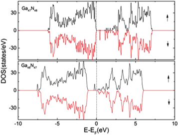
Figure 4. The TDOS of GaN NW with one VGa (Ga47N48) and with one VN (Ga48N47).
Download figure:
Standard image High-resolution imageTo understand the mechanism behind this magnetism, we have calculated the electronic structure of Gd-doped GaN NWs in presence of both VGa and VN, as shown in figure 3 (middle and bottom panels, respectively). The DOS for the Gd-doped GaN NW without any vacancy is plotted in figure 3 (top panel). It can be noted that VGa introduces a defect state in the minority spin near the EF and below the VBM, whereas positions of 4f states remain unaltered. It is well known that hybridization of defect levels with that of impurity atom near the EF and below the VBM leads to ferromagnetic coupling in Gd-doped GaN. The inset in the middle panel of figure 3 shows the projected DOS, which indicates the hybridization between the defect bands introduced by VGa and that of Gd (4f and 5d) in the Ga46N48Gd NW. It can be seen that the hybridization between the Ga d and N p states and Gd (4f and 5d) states in the spin down channel contributes to the additional states near the EF. The Gd 4f and 5d states in the VB show a clear spin up–spin down splitting. In the presence of VGa, spins introduced by these additional defect levels interact with the Gd spin ferromagnetically, resulting in a slight rise in the Gd magnetic moment, simultaneously polarizing the nearby N atoms, thus increasing the total magnetic moment of the system by about 3 μB. Henceforth, possibility of a p–d exchange interaction arises between d orbitals of Ga and Gd and p orbitals of N. However, the presence of delocalized carriers is less likely to induce magnetism and therefore Zener's direct exchange mechanism [42] cannot be the cause of the observed FM in GaN NWs. In the present context, the magnetic polarization at the N sites caused by the Gd-VGa complex assists in stabilizing FM. Furthermore, it is not possible for the s–f exchange interactions to occur, as the Gd atoms stay apart and prefer not to aggregate. The Gd f and d states overlap well with the defect band near the EF and VBM, as shown in the inset in the middle panel of figure 3. Therefore, our study establishes the idea of cation vacancy-induced FM in RE-doped GaN NWs due to the increased hybridization between the p states of Ga and N with d and f states of Gd [22]. Consequently, the mechanism behind FM in Gd-doped GaN NWs can be ferromagnetic superexchange-like interactions [19] mediated through the N sites.
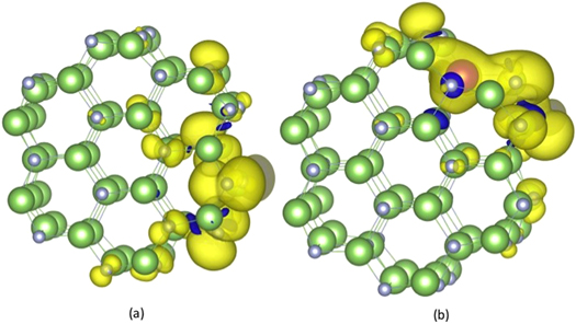
Figure 5. The spin density plot for (a) GaN NW in presence of VGa (Ga47N48) and (b) Gd-doped GaN NW in presence of VGa (Ga46N48Gd). The green and white spheres represent Ga and N atoms, respectively, whereas the red spheres in (b) represents Gd atom.
Download figure:
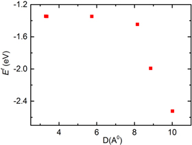
Standard image High-resolution imageTo examine the strength of ferromagnetic exchange coupling and to demonstrate the existence of long-range magnetic interactions, we have introduced two Gd atoms, while removing two Ga atoms from the NW supercell. Introducing more than one Gd atom will also provide valuable insight into the clustering tendency of dopants in the NW. The Ef for a pair of Gd atoms is calculated according to equation (1) and the results are plotted in figure 6. Interestingly, the Ef results show that no Gd aggregation can take place in the NWs. The Gd atoms prefer to stay apart as the Ef decreases with the increase in distance (D) between Gd atoms, as shown in figure 6. This observation is in line with the available experimental findings indicating that Gd atoms distribute homogeneously in wurtzite GaN without clustering [4, 18]. Further, to investigate the stability of RTFM, the total energy difference (ΔE) between the ferromagnetic (FM) and antiferromagnetic (AFM) configurations of Gd atoms in the NW is calculated (ΔE = EFM − EAFM). A positive value of ΔE implies that Gd atoms prefer FM coupling in the NW and vice versa. The calculated value of ΔE is only about 1.1 meV, signifying the paramagnetic nature of Gd–Gd interactions in the Ga46N48Gd2 NW. However, introducing one hole (additional positive charge) by reducing the total number of valence electrons results in weak FM coupling, with ΔE of 12.4 meV, which concurs with the findings in bulk GaN, where the presence of holes is shown to enhance the ferromagnetic coupling [19]. By introducing one VGa in the Ga46N48Gd2 NW, a significant increase in magnetic coupling is observed at the nearby atomic sites. A single VGa introduces three holes, which are in a triplet magnetic ground state and strengthens the FM of the system. The calculated value of ΔE is 76.4 meV, which is strong enough to stabilize RTFM, since a minimum ΔE of 30 meV is required to establish magnetic coupling against thermal fluctuations. These findings are line with Gd doped bulk GaN [19]. On the other hand, negligible magnetization is achieved by the introduction of VN and electron carriers, in accordance with previous studies, which showed that VN and electron carriers are not involved in mediating ferromagnetic interactions in Gd:GaN [22]. The behavior of VN in Gd-doped GaN can be explained from the TDOS perspective, as shown in figure 3 (bottom panel). In presence of VN, the VBM shifts away from the EF and the GaN NW shows semi-insulating nature. The DOS reveals that the 4f majority levels are shifted well below the VBM, whereas the minority spin states move closer to the EF. However, at EF, spin up and spin down DOS are symmetric, giving rise to zero spin polarization in the system. Thus, the proposition that electron-mediated FM in Gd-GaN stems from s–f or s–d coupling interaction [23] is not valid in the present context, as the possible origin of electron carriers is VN, and such vacancies are not favorably forming in the NW and induce zero spin polarization. Hence, it can be concluded that the large magnetic moment contributed by the Gd atom, combined with the spin polarization induced by the VGa to the N sites, strengthens the magnetic coupling in the NW.
Figure 6. The formation energy (in eV) for two Gd atoms in GaN NW (Ga46N48Gd2) with their distance of separation (in Angstrom).
Download figure:
Standard image High-resolution image
4. Conclusions
Investigations on GaN NWs in presence of intrinsic and extrinsic defects were carried out. Our findings showed that Gd atoms do not prefer to cluster in the NW and exhibit paramagnetic coupling in the absence of intrinsic defects. Ef of point defects is reduced in the GaN NW compared to bulk. Moreover, VGa is more stable than VN and induces FM in the NW. The Gd atoms reduce the Ef of point defects further and FM is strengthened by the Gd-VGa complex defects. Our study thus emphasizes the importance of the presence of additional hole carriers in establishing RTFM in Gd-doped GaN NWs.