

Abstract
In this work, design and optimization of ultraviolet sensors based on ZnS nanoparticles with the focus on the effect of annealing temperature on optical properties of zinc sulfide were carried out. Synthesis of ZnS nanoparticles was performed using a chemical deposition method and annealing process was followed at 300 °C, 500 °C and, 700 °C under flow of argon. Scanning electron microscopy indicated that by increasing the annealing temperature, the particle size of ZnS nanostructures is increased. Differential thermal analysis showed that the temperature range of phase transformation in ZnS nanostructures is at 300 °C–450 °C. X-ray diffractometry demonstrated a phase change from zinc blende to hexagonal wurtzite at the temperature of 500 °C. The UV-visible spectra of the ZnS samples indicated an increase in light absorption of ZnS nanostructures regarding to the phase transformation at 500 °C. Photoluminescence (PL) study also demonstrated a slight blue-shift in PL peak position of the sample that was annealed at 500 °C which is attributed to the higher optical band gap of this sample. Moreover, the intensity ratio of UV to visible peak is the highest for this sample showing an enhancement in optical properties of ZnS nanostructures which is suitable for fabrication of visible-blind UV detectors. For studying the influence of annealing temperature on optoelectrical properties of UV sensors based on ZnS nanostructures, metal-semiconductor-metal devices were fabricated using deposition of interdigitated Schottky contacts on different ZnS samples. The suitable optical and structural properties of the optimum sample including increasing the electron-hole pairs under UV illumination was manifested in optoelectrical characteristics of ultraviolet detectors based on ZnS sample which was annealed at 500 °C. For this sample, the sensitivity under UV radiation was enhanced by 6.9 times compared to the other ZnS samples.
Export citation and abstract BibTeX RIS
Introduction
Semiconductor nanostructures were interesting in recent decades, because of their tunable electronic and optical properties [1, 2]. Zinc sulfide (ZnS) as a primary semiconductor has a high band gap (3.76 and 3.7 eV for hexagonal wurtzite and cubic zinc blende, respectively) [3]. Zinc sulfide nanoparticles are one of the important semiconducting compounds due to their potential applications including electroluminescence [4], optical detectors [5] electrochemical sensors [6], photocatalysis [7], and light emitting diodes [8]. Variation in synthesis methods is one of the advantages of ZnS over other semiconductor materials. Different techniques which have been reported for synthesis of ZnS nanoparticles are including hydrothermal [9], solvothermal [10], sonochemical [11], chemical bath deposition [12] and chemical vapor deposition [13]. ZnS is a suitable candidate for use in ultraviolet detectors. Ultraviolet radiation with the wavelength range of 200–400 nm has an energy range of 3–12.4 eV which is divided into three ranges. The longest wavelength related to UV-A, which has a wavelength in the range of 320–400 nm. Usually, in the Earth's atmosphere, this type of ultraviolet radiation is found. Another subdivide of ultraviolet radiation that is absorbed by sunscreen and is harmful to the skin is called UV-B, which its wavelength range is 320–280 nm. The third subdivided of ultraviolet radiation that absorbed by the Earth's atmosphere is UV-C, with wavelengths ranging from 280 to 200 nm. The matching of the bandgap of the ZnS with the energy of ultraviolet radiation has made it a suitable material for use in the photodetector in this range [14].
The morphology of ZnS and zinc oxide (ZnO) nanostructures is comparable but due to inherent defects such as oxygen vacancy, light absorption in ZnO nanostructures is limited. Moreover oxygen vacancies in ZnO cause low resistance, low response and unstable photocurrent under ultraviolet radiation. But ZnS has high surface resistance and fast response to ultraviolet radiation. Thus it has a higher potential for use in ultraviolet detectors [15].
ZnS has two different allotropes; hexagonal wurtzite (WZ) and cubic zinc blende (ZB). The structural difference between ZB and WZ results in different optical and electrical properties of ZnS allotropes. For instance the optical band-gap of ZnS is different for ZB and WZ allotropes [16]. The density functional theory (DFT) can demonstrate these differences and show the distinction between the rates of dispersion for valence bands and conduction bands for zinc blende and wurtzite structures [17]. In a research by Trang et al, it was found that the increase in ZnS band-gap occurs for two reasons: crystal field splitting between bands and spin–orbit interaction [18]. Structurally, ZB has a better structural symmetry than WZ, which is suitable for applications that need higher values of light transmittance, while WZ structure absorbs light more than ZB. This potential of absorption for WZ structure can provide higher photo-generated electrons and enhance the performance of photodetector [19]. For using ZnS as a photodetector, one of the most effective methods to improve the photocurrent is to use ZnS as a single-crystal and in thin films. Obtaining ZnS as a single-crystal is very costly and sophisticated. An alternative method for enhancement in the electrical characteristics of fabricated photodetectors based on ZnS is the use of nanostructures such as nanoparticles, nanobelts and, nanotubes [20]. The nanostructures have higher specific surface area and can capture the incident light and generate higher amount of photo-generated electron-hole pairs.
In this study, chemical deposition method was used as a controllable, repeatable and low-cost method to synthesize good-quality nanoparticles of ZnS. The effect of annealing process on structural phase transformation of zinc sulfide nanostructures was studied. The structural phase change which was caused by annealing process at elevated temperatures had influence on the optical and electrical properties of zinc sulfide nanostructures. For studying this phenomenon, ZnS nanostructures which were annealed at different temperatures were applied as a substrate for design and fabrication of metal–semiconductor–metal (MSM) ultraviolet sensors with Schottky contacts. The effect of annealing temperatures on electrical characteristics of designed ultraviolet sensors based on ZnS nanoparticles was studied.
Experimental activities
Chemical deposition method was used in order to synthesize ZnS nanoparticles. Zinc acetate dehydrates (Zn (CH3COO)2 2H2O) and sodium sulfide (Na2S) was the chemical precursors used in this reaction. 0.1 M zinc acetate and 0.3 M sodium sulfide were dissolved in 50 ml of deionized water, separately. The sodium sulfide solution was then poured into zinc acetate under continuous stirring for 20 min and the temperature of chemical reactions was set at 60 °C. After the reaction was completed, a white precipitate was formed. The obtained precipitate was then washed by adding ethanol and deionized water and was dried for 24 h at 60 °C. The obtained powder containing of ZnS nanoparticles was then heated at 300, 500 and 700 °C with annealing rate of 5 °C min−1 under inert atmosphere of argon for 1 h.
A monocrystalline p-type Si wafer doped by the addition of boron with resistance of 4 Ω/cm2 and thickness of 330 μm was sliced in 2 × 2 cm2 and was used as substrate. For removing chemical contaminations from Si surface, the samples were cleaned for 15 min using a solvent clean containing 5 ml of acetic acid, 2 ml of hydrofluoric acid, and 25 ml of nitric acid. The Si substrates were then eluted with distilled water and dehumidified under flow of nitrogen atmosphere. For growing ZnS thin film on silicon samples, Doctor blade method was utilized. Here, ZnS nanoparticles (4 g) were added in 1 ml of distilled water for obtaining an appropriate solution. A flexible blade was utilized to spread the chemical solution to the whole surface of the Si samples and clean the extra amount of chemicals from the substrate. Then, the remaining water was evaporated by warming the samples at 60 °C for 1 h leading to the formation of a homogenous thin film with the thickness of ∼22 μm. For fabrication of MSM UV sensors, two interdigitated finger electrodes of gold containing four fingers for every electrodes were deposited on top of all substrates by sputter deposition equipment (model NSC-DSR1). The thickness of electrodes was about 100 nm. The dimension of finger electrodes was 3 × 4 mm with finger spacing of 0.4 mm. In order to reduce the atomic mismatch between the ZnS layer and gold electrodes and for making suitable Schottky junctions, substrates were heated in a tube furnace under nitrogen flow for 30 min at 300 °C. The optoelectrical characterizations of designed UV sensors including current-voltage (I–V) properties were studied at RT with integrated computer-controlled Source-Measure equipment (Keithley 2400). For all of the fabricated devices, the current densities were obtained in dark (Id) and under UV illumination (Iph) with a power of 10 mW cm−2 and wavelength of 260 nm which was generated from a UV source (Philips 8 W TUV-C). A precise x-ray diffractometery (XRD) system (Philips DW-3710) was utilized for analyzing the structural characteristics of the samples. The photoluminescence (PL) spectroscopy was carried out using a Perkin-Elmer spectrometer (LS-5) at RT.
Results and discussion
Structure and morphology
Figure 1 demonstrates the differential thermal analysis (DTA) curve for as-synthesized ZnS nanostructures. A low-intensity exothermic peak is observed at a temperature range of 300 °C–450 °C which expresses phase transformation of zinc sulfide from cubic to hexagonal. An exothermic peak is observed at 630 °C which is due to the oxidation of zinc sulfide and its conversion to zinc sulfate or zinc oxide. According to the thermal gravimetric analysis (TGA) curve, weight loss occurs in two stages; the first stage is at temperatures below 160 °C which is about the reduction of 37.5% of the sample weight. It is due to the evaporation of water which has been physically absorbed. The second stage of weight loss occurs at a temperature range of 180 °C–800 °C, which can be attributed to structural dehydration, phase transformation from cubic to hexagonal, and sulfur removal from zinc sulfide structure. These results are in good agreement with the results obtained in previous studies [21].

Figure 1. DTA and TGA curves for synthesized ZnS nanostructures fabricated via chemical deposition method.
Download figure:
Standard image High-resolution imageFigure 2 demonstrates the x-ray diffraction patterns related to the deposited samples. Based on the reference card No. 01-077-2100, the XRD peaks at 2θ values of 28.53°, 47.45°, and 56.30° are referring to the (111), (220) and (311) crystal orientation of zinc blende ZnS, respectively. For annealed sample at 300 °C, there is no phase transformation and the zinc blende phase is remaining. The only change is increasing the peak intensity due to an improvement in crystal quality. The annealed sample at 500 °C shows new peaks that demonstrates a phase change in ZnS crystal structure at this temperature. By comparing with the reference card No. 01-089-2191, it is obtained that the peaks at 2θ positions of 26.93°, 28.48°, 30.54°, 39.62°, 47.53°, 51.79°, and 56.41° are related to the (100), (002), (101), (102), (110), (103) and (112) crystal orientation of hexagonal wurtzite ZnS, respectively. For the sample annealed at 700 °C, new peaks are shown in 2 θ positions of 31.37°, 34.36° and 36.20° that is referred to (100), (002) and (101) lattice planes, respectively based on reference card No. 01-080-0074. It is found that these peaks are related to a hexagonal phase of ZnO in this sample. The appearance of ZnO peak at 700 °C is in good conformity with the exothermic peak at 630 °C in DTA results (figure 1). It shows the oxidation of zinc sulfide and its conversion to zinc oxide at 700 °C which is considered impurity and it is not desirable.
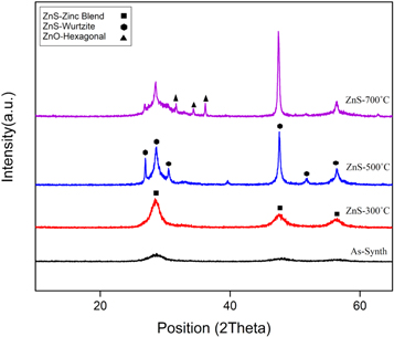
Figure 2. XRD patterns for as-synthesized ZnS, annealed ZnS at 300 °C, 500 °C and 700 °C.
Download figure:
Standard image High-resolution imageThe crystallite size of ZnS nanostructures with different annealing temperatures is obtained using Williamson-Hall equation, as follows;

here θ is the position of peaks (in degrees), λ is the wavelength of the x-ray in Å, β is the full width at half maximum (FWHM) in radians, ε is the residual strain in the lattice, d is the average size of the crystallites in Å and A is a constant number. The calculated results which are shown in table 1, demonstrate that in ZnS structures, the crystallite size is increased with an increase in annealing temperature.
Table 1. The structural properties of as-synthesized and annealed ZnS nanostructures and Calculated Bandgap for ZnS Samples.
| Sample | Peak position (2θ) | FWHM | Crystallite size (nm) | Band gap (eV) |
|---|---|---|---|---|
| ZnS (As-synthesized) | 28.53 | 0.629 | 4.6 | 3.88 |
| ZnS (Annealed at 300 °C) | 28.53 | 0.392 | 10.7 | 3.76 |
| ZnS (Annealed at 500 °C) | 47.54 | 0.227 | 24.4 | 3.80 |
| ZnS (Annealed at 700 °C) | 47.53 | 0.171 | 33.5 | 3.62 |
Figure 3 shows the FESEM micrographs for ZnS substrates with different annealing temperature. The morphology of different samples indicates that the average particle size of as-synthesized sample is 7 nm and it is increased by annealing process. For the sample annealed at 300 °C, the average size is 24 nm and it is reached to 35 nm and 74 nm for the samples annealed at 500 °C and 700 °C, respectively. Moreover, the morphology results indicate that with increasing the annealing temperature, agglomeration of ZnS nanoparticles is occurred.
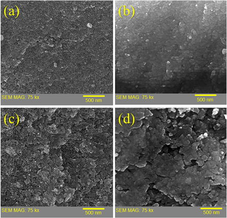
Figure 3. FESEM micrographs of ZnS nanostructures; (a) as-synthesized, (b) annealed at 300 °C, (c) annealed at 500 °C, (d) annealed at 700 °C.
Download figure:
Standard image High-resolution imageOptical properties
Figure 4 shows the UV–vis analysis of zinc sulfide samples that were annealed at different temperatures. For the sample with annealing temperature of 300 °C, absorption is the lowest compared to the other synthesized samples. The minimum absorption coefficient of this sample is due to an improvement in its crystalline structure, as indicated in the XRD pattern. The cubic zinc-blend structure has a better structural symmetry compare to the hexagonal wurtzite structure. Therefore, due to the wurtzite structure of the sample with annealing temperature of 500 °C, the absorption coefficient is increased. Based on FESEM micrographs, by increasing the annealing temperature to 700 °C, the agglomeration of ZnS nanoparticles was occurred. Therefore, by increasing the particle size of this sample, the expose area is reduced and light trapping at ZnS surface is decreased. Thus, the absorption coefficient of ZnS nanostructures with annealing temperature of 700 °C is lower than the one with annealing temperature of 500 °C.
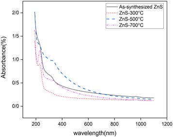
Figure 4. UV–vis absorbance spectra for as-synthesized and annealed ZnS nanostructures.
Download figure:
Standard image High-resolution imageThe optical bandgap for different ZnS samples is calculated using the following equation;

where λabs is the absorption wavelength, h is the Planck constant, ν is the incident light frequency and Eg is the band gap. Accordingly, for each sample, the band gap was calculated and reported in table 1.
The optical properties of nanomaterials are affected by the size of particles. The bandgap of as-synthesized ZnS nanostructure (3.88 eV) is higher than the one for bulk ZnS (3.72 eV). This increase can be justified by the quantum confinement effect, which occurs in nanomaterials when the particle size becomes comparable with Bohr radius of exciton [22]. The Bohr exciton radius of ZnS is ∼2.5 nm [23]. Therefore, the band gap of synthesized ZnS samples can be derived according to the following equation;

where, Eg(bulk) is the energy gap in bulk state, h is the Planck's constant, r is the radius of the nanoparticle,  is the effective mass of the electron,
  is the effective mass of the hole, e is the electron charge, ε is the dielectric coefficient of ZnS and ε0 is vacuum permittivity. For the ZnS sample that was annealed at 300 °C the bandgap decreased to 3.76 eV. This decrease is due to an increase in the size of ZnS nanoparticles. The bandgap of ZnS that was annealed at 500 °C is increased to 3.80 eV. This increase can be attributed to the phase transformation from zinc-blend to the wurtzite. In general, the bandgap of wurtzite (3.77 eV) is higher than the one for zinc-blend (3.72 eV). For ZnS that was annealed at 700 °C, the bandgap is decreased, which is due to an increase in particle size when higher annealing temperature is applied.
Figure 5 illustrates the PL spectra of zinc sulfide nanostructures that were annealed at different temperatures. For excitation of ZnS nanostructures, a laser beam with a wavelength of 300 nm was applied. Here, the electron-hole recombination is due to the presence of zinc vacancy as the acceptor and sulfur vacancy as the donor. The first peak at 421 nm is related to the electron-hole recombination in sulfur vacancy. Another peak at 492 nm is attributed to the electron-hole recombination in zinc vacancy. Because the energy level of the sulfur vacancy is near to the conduction band, it radiates at shorter wavelengths, but the energy level of the zinc vacancy is near to the valence band and therefore it radiates at longer wavelengths. A low-intensity peak, at the wavelength of 536 nm, indicates the transition from the energy level of sulfur vacancy and interstitial sulfur atoms. In all of samples, by increasing the annealing temperature, the PL intensity is enhanced which is due to an increase in sulfur vacancy when higher temperature is applied. The sulfur vacancies are the sites for electron-hole recombination and they can generate higher PL intensity. A slight blue-shift in PL peak position of the sample that was annealed in 500 °C is attributed to the higher optical band gap of this sample and is in good agreement with the UV–vis results. Moreover, the full-width at half maximum (FWHM) of PL peak is the lowest for the sample with annealing temperature of 500 °C. The FWHM of the PL peak is a good indicator of optical quality of the material, because the PL peak can be widened by the structural defects and impurities [24]. Therefore, the concentration of impurities decreased in the sample with annealing temperature of 500 °C. The optical properties of ZnS nanostructures with different annealing temperatures are summarized in table 2. The intensity ratio of UV to visible peaks is the highest for sample with annealing temperature of 500 °C showing that this sample is suitable for fabrication of visible-blind UV detectors.
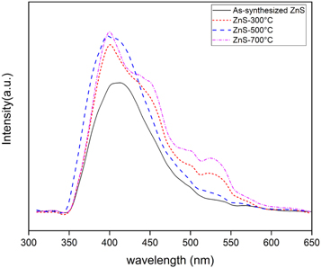
Figure 5. PL spectra for as-synthesized and annealed ZnS under laser radiation with the wavelength of 300 nm for excitation.
Download figure:
Standard image High-resolution imageTable 2. The PL results for as-synthesized and annealed ZnS nanostructures.
| Sample | Peak position (nm) | FWHM (nm) | The intensity ratio of UV to visible peaks |
|---|---|---|---|
| ZnS (As-synthesized) | 421 | 90 | 7.36 |
| ZnS (Annealed at 300 °C) | 400 | 93 | 4.1 |
| ZnS (Annealed at 500 °C) | 396 | 88 | 9.37 |
| ZnS (Annealed at 700 °C) | 402 | 95 | 3.34 |
Optoelectrical properties
Figure 6 demonstrates the current-voltage characteristics of ZnS substrates with different annealing temperatures. The voltage bias was swiped from −5 V to 5 V and the current density was measured. The obtained optoelectrical properties of different UV sensors are summarized in table 3. The sensitivity of designed UV sensors was derived from the current-voltage curves by utilizing the following equation [25];

where Id and Iph are the dark current and photocurrent, respectively. The sensitivity of fabricated ultraviolet sensors as a function of annealing temperature is shown in figure 7.
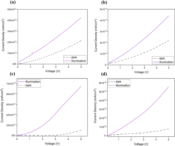
Figure 6. The current–voltage curves for UV sensors based on different ZnS nanostructures; (a) as-synthesized, (b) annealed at 300 °C, (c) annealed at 500 °C, and (d) annealed at 700 °C.
Download figure:
Standard image High-resolution imageTable 3. The optoelectrical properties of fabricated UV detectors based on as-synthesized and annealed ZnS samples with different annealing temperatures.
| Sample | Sensitivity | Photocurrent density at 5 V (mA cm−2) |
|---|---|---|
| ZnS (As-synthesized) | 0.909 | 4.22 × 10⁻³ |
| ZnS (Annealed at 300 °C) | 1.75 | 4.41 × 10⁻³ |
| ZnS (Annealed at 500 °C) | 6.33 | 8.38 × 10⁻³ |
| ZnS (Annealed at 700 °C) | 5.87 | 5.47 × 10⁻³ |

Figure 7. The sensitivity of UV sensors based on ZnS samples with different annealing temperature.
Download figure:
Standard image High-resolution image
Here, for the as-synthesized sample, there is a negligible variation between photocurrent and dark current (figure 6(a)). However, after annealing process, this difference is increased and the sensitivity is enhanced. Due to the increase in light absorption for the sample with annealing temperature of 500 °C (based on figure 4), the rate of electron-hole pair generation under UV irradiation is maximum for this sample. Subsequently, more photogenerated electrons are produced when this sensor is under exposure of UV illumination. Thus, the photocurrent and sensitivity is enhanced for the sensors based on ZnS nanostructures with annealing temperature of 500 °C.
Overall, the obtained results indicate that annealing process has a significant effect on sensitivity of UV detectors based on ZnS nanostructures. Based on XRD results, due to a phase change in crystal structure of the sample with annealing temperature of 500 °C, the rate of light absorption is increased and ratio of photocurrent to dark-current is enhanced. Therefore, the sensitivity is improved for the sensor with this annealing temperature. Applying higher annealing temperature (700 °C) leads to the agglomeration of ZnS nanoparticles and reduction of surface expose area. Therefore, the absorption coefficient of the sample with annealing temperature of 700 °C is decreased. Thus, the reduction in the amount of photo-generated electrons causes a decrease in the sensitivity of UV sensor based on this sample.
Conclusions
Synthesis and development of ZnS nanoparticles were performed using chemical deposition technique. Annealing process was followed in order to enhance the optical and structural properties of ZnS samples. At annealing temperature of 500 °C, the structure of ZnS was changed from zinc blende to wurtzite. An increase in the size of ZnS nanoparticles was demonstrated in FESEM micrographs. The results showed that due to the phase change at 500 °C, the absorption rate is enhanced and the PL intensity is increased. Moreover, it was affirmed that the rate of electron-hole generation is increased at this annealing temperature. The optoelectrical characteristics of ultraviolet sensors were studied in dark and under UV illumination. The results indicate that for the sensor with annealing temperature of 500 °C, higher photogenerated electrons are produced under UV exposure. Thus, the sensitivity of this sample is higher compared with other ZnS samples. It demonstrates an improvement in optoelectrical properties of ZnS nanostructures with wurtzite structure in UV detection applications.
Acknowledgments
This research was supported by the Materials and Energy Research Center [Grant No. 771394077].