
Abstract
The device dimensions have been consistently scaling down since many developing technologies need smaller and faster integrated circuits for advancement and improvement in both performance and device density. Device dimensions have been decreased drastically from micron to sub nanometer regime. Traditionally, miniaturizing and performance improvement was obtained by tweaking the MOSFET- reducing the channel lengths and gate oxide thickness, increasing dielectric constants etc Unfortunately at 22 nm node it reached a dead end. However, at 22 nm node the tri-gate FinFET introduced by Intel Corporation have provided many possibilities for scaling the dimensions with satisfactory device performance. Further, the gate all around (GAA) carbon nano tube field effect transistor (CNTFET) provides high gain, high trans-conductance, reduced short channel effects and conditions for scaling the technology to sub nano scale. Due to surround gate structure this GAA CNTFET offers better control with integration of high_k stacked dielectric wrapped around the channel. In this paper, first properties of Carbon nanotube (CNT) have been comprehensively studied for various chirality and diameter and parameters viz. Density of States (DoS) and Band gap (Eg) are extracted by using MedeA tool's VASP 5.3 module. The various CNT chirality have been optimized and the extracted parameters used to model and simulate CNTFET using Silvaco's Devedit3D, Atlas and Atlas3D modeling and simulation modules. The device input (ID-VGS ) and output (ID-VDS) characteristics have been intensively studied and parameters including ION /IOFF ratio, DIBL, sub threshold slope extracted and compared with the conventional devices. The GAA CNTFET device at 0.8 V supply voltage exhibits threshold voltage (VTH) 0.254 V, drain induced barrier lowering (DIBL) 72 mV/V, sub-threshold swing (SS) 63.29 mV/dec, and ION/ IOFF ratio 7.17e + 06. The results demonstrate improvement in device parameters for the GAA CNTFET device as compared to bulk silicon and FinFET devices.
Export citation and abstract BibTeX RIS

Original content from this work may be used under the terms of the Creative Commons Attribution 4.0 licence. Any further distribution of this work must maintain attribution to the author(s) and the title of the work, journal citation and DOI.
1. Introduction
The modern industry of semiconductors has been working on its unique feature to double the transistor count every two years according to Moore's Law for last six decades. However, the roadmap for semiconductor technology development suggests that conventional MOSFET technology is reaching its fundamental physical limits. It is therefore a time to review state-of-the-art, potential capabilities of MOSFET devices to meet the various scaling targets and market requirements [1]. The scaling of device dimensions and supply voltage are the major challenges for future high performance and low power nano scale devices. The device and system optimization are to be done in terms of high performance, low power, less area and reduction in overall cost and of course the time to market. However there may be tradeoff between the various optimization measures for a particular application. In the nanoscale device, with the scaling of channel length, the device behavior also departs from its usual characteristics and short channel effects comes into play [2]. The device channel mobility becomes field dependent with increase in electric field which results in velocity saturation. Further, hot-carriers injected into the thinner dielectric leads to charge trapping into the dielectric which causes the change in threshold voltage and trans-conductance degradation at high fields [3]. The drain induced barrier lowering (DIBL), impact ionization, sub-threshold swing (SS) and the quantum mechanical effect like band to band tunneling, gate, source and drain tunneling also degrades the device performance [4, 5]. Further, increase in sub-threshold swing (SS) of a field effect transistor represents loss of gate control, mainly due to quantum mechanical tunneling of charges through the energy barrier of channel and/or weakened electrostatics in the scaled channel of nano scale device [6, 7]. The tri-gate / FinFET was introduced in Ivy Bridge series of processors by Intel Corporation in 2011 to meet the industry demand [8].
In this FinFET device source and drain regions are connected via thin fins used as a channel and the gate wraps three sides of the fin for better control of the flow of charge carriers which further reduces the leakage current [9, 10]. However, FinFET due to its vertical and rectangular geometry holds issues such as corner effects, parasitic capacitance, gate electrostatics and process complexity etc [11]. The novel device such as CNTFETs with surround gate also known as gate all around geometry with their quasi ballistic charge transport could be better choice for future semiconductor technology [7, 12].
The Carbon Nanotube as a channel in CNTFETs could be better choice for scaling the technology and to minimize short channel effects (SCEs) [13]. The study has been carried out using CNT as a channel material. The higher current density in CNT is because of ballistic transport of charge carriers in device channel region and hence CNT as a channel give good performance because of higher carrier mobility of CNT as compared to silicon as a channel material.
2. Carbon nanotube as a device channel
The Carbon nanotubes offer some special properties and unique features that have good potential for nano scale devices. The CNTs are good candidate for device engineers as conducting CNTs can be used for interconnects and semiconducting CNTs find major applications in CNTFETS for robust performance devices [13, 14]. A carbon nanotube is a rolled graphene sheet along a particular direction to form a tube having diameter in the range 1 nm to 100 nm. The direction in which graphene sheet is rolled can be defined as a vector as:

where are positive integers and are lattice unit vectors which decides chirality of nanotube. Depending upon the chiral number or chirality which indicates the atomic arrangement, the carbon nanotube can be made of any form like armchair , zigzag () and chiral for all other integer values of . Also, CNT can be made either conducting or semiconducting decided by the chirality, the tube is conducting if (n1−n2) is divisible by 3 and if (n1−n2) is not divisible by 3 it is semiconducting. The CNT diameter () is the key parameter which affects the conductivity of channel and also the contact resistance in CNTFET, so it is crucial to optimize the CNT diameter for their use in CNTFETs to maintain the gate control and electrostatics for optimum device performance.
The CNT becomes more conducting at larger diameter which degrades the power handling capacity and hence the gate electrostatics [15]. Also, the leakage current and hence the power consumption increases with decrease in band gap () or decrease in threshold voltage () of CNTFET device [16, 17].
The band gap of carbon nanotube is dominantly dependent on the CNT diameter that governs various electrical and physical properties of the CNT and hence CNTFET. The band gap (Eg) of CNT can be calculated as [18, 19]:

where is the carbon-carbon bond length and is carbon bond tight binding energy parameter and is the diameter of carbon nanotube.
The semiconducting CNTs with same chirality have same density of states and similar other properties. Also, some other parameters such as effective mobility (), inversion capacitance (), subthreshold coefficient (), strong inversion threshold voltage (), carrier velocity (), source resistance () and drain resistance are dependent to CNT diameter. In CNTFET device threshold voltage can be determined as [18, 21]:

where is the coefficient of DIBL, q is electron charge, where and are source and drain resistances respectively.
3. The gate all around (GAA) carbon nano tube field effect transistor (CNTFET)
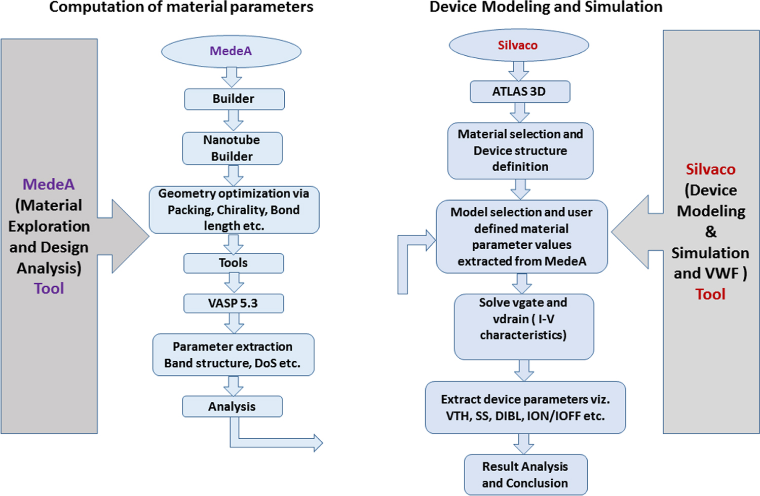
The CNTFET's are ballistic devices using a single or an array of CNTs as a channel material instead of bulk silicon as in conventional MOSFETs [19, 21, 22]. The device simulators like Silvaco TCAD in their material library does not contain novel materials like Graphene, CNT etc to model and simulate the device structures with these materials. However if their material parameters can be obtained and introduced in to the material library of the tool then Silavco TCAD tool can be used to design and study the features of the devices using these materials. The band structure and hence band gap and density of states variation with chirality and diameter of CNT which can influence the device performance can be simulated and investigated for CNTFET devices using MedeA tool. The research process flow as illustrated in figure 1, is based on modeling and simulation of semiconductor materials and devices with gate all around geometries for high performance nano scale applications.

Figure 1. Summary of research process flow.
Download figure:
Standard image High-resolution imageThe semiconducting CNT has been simulated and investigated using Nanotube Builder module of MedeA tool and parameters like band gap, density of states have been extracted using VASP module. The extracted parameters are then used in Silvaco's ATLAS 3D module to define new material which is not available in its library and this new material has been used to model novel GAA CNTFET device.
3.1. Density functional theory (DFT) and investigations on material parameters
The Density Functional theory (DFT) is a quantum mechanical modeling method for obtaining approximate solution to Schrodinger wave equation to get the wave function of a many-body system. The MedeA tool has been designed to give quick access to various materials property data both by mining experimental data and by computing various properties where experimental data for novel materials is scarce or only partly available for critical investigations. The MedeA modules use Vienna Ab initio simulation package (VASP) as a Density Functional Theory (DFT) solver for studying the various properties like electrical, mechanical, optical, magnetic, chemical and thermal of different materials [23]. The basic electrical properties such as band structure, density of states (DoS) which decides the electrical conductivity of material used for device simulation can be estimated using this tool.
3.2. Simulation and estimation of band gap and density of states (DoS)
The semiconducting carbon nanotubes (CNTs) have been simulated and intensively studied using MedeA VASP tool and then investigated to optimize the tube chirality and diameter for band gap and DoS measurements which are further used for CNTFET device modeling and simulation using Silvaco TCAD. The increase in tube chirality causes decrease in device threshold voltage and hence the leakage current increases so low tube chirality is desired for CNT as channel material in CNTFET devices [16]. The various parameters estimated for different CNT chirality are listed in table 1. The band gap for optimized nanotube chirality and/or diameter semiconducting CNT (6, 2) has been measured as 0.61 eV and density of states NC = 8.88e20, NV = 7.37e19.
Table 1. Estimation of CNT diameter and Band gap for different CNT chirality using MedeA VASP tool.
| S.N. | CNT Chirality (n1, n2) | CNT Diameter (nm) | Band gap (eV) |
|---|---|---|---|
| 1 | 6, 2 | 1.41 | 0.61 |
| 2 | 10,0 | 1.69 | 0.51 |
| 3 | 11,0 | 1.76 | 0.49 |
| 4 | 13,0 | 1.91 | 0.45 |
| 5 | 14,0 | 2.27 | 0.38 |
| 6 | 16,0 | 2.87 | 0.3 |
The simulation results shows that the electrical conductivity of the semiconducting CNT is high and almost constant for wide range of temperature which indicates its thermal stability for high performance nano scale applications.
The gate all around CNTFET device has been modeled and simulated using the device parameters as listed in table 2. The device having channel length 14 nm, integrated gate dielectric thickness 5 nm and other parameters for semiconducting CNT of chirality (6, 2) as a device channel.
Table 2. Various parameters used for modeling and simulation of CNTFET device with surround gate geometry.
| The gate all around (GAA) carbon nano tube field effect transistor (CNTFET) | ||
|---|---|---|
| Device parameters | Brief description | Values |
| Ch(n,m) | CNT chirality | (6,2) |
| DCNT | CNT diameter | 1.41 nm |
| L | Channel length | 14 nm |
| Eg | Band gap | 0.61 eV |
| DOS (NC) | Density of states in CB | 8.88e20 |
| DOS (NV) | Density of states in VB | 7.36e20 |
| Toxi | Inner oxide thickness (SiO2) | 2 nm |
| Koxi | Inner oxide dielectric constant | 3.9 |
| Toxt | Stacked outer gate oxide (HfO2) thickness | 3 nm |
| Koxt | Stacked outer gate oxide (HfO2) dielectric constant | 25 |
| NSD | Source/ Drain Doping | 1e + 20 cm3 |
| KCNT | CNT dielectric constant | 1 |
| Eea | Electron affinity | 3.2 eV |
| Φm | Metal gate work function | 5.22 eV |
| 𜺠| Permittivity | 9.7 F m−1 |
| μn | Mobility of electrons | 8e4 cm2/v-s |
| μp | Mobility of holes | 8e4 cm2/v-s |
| T | Temperature | 300 K |
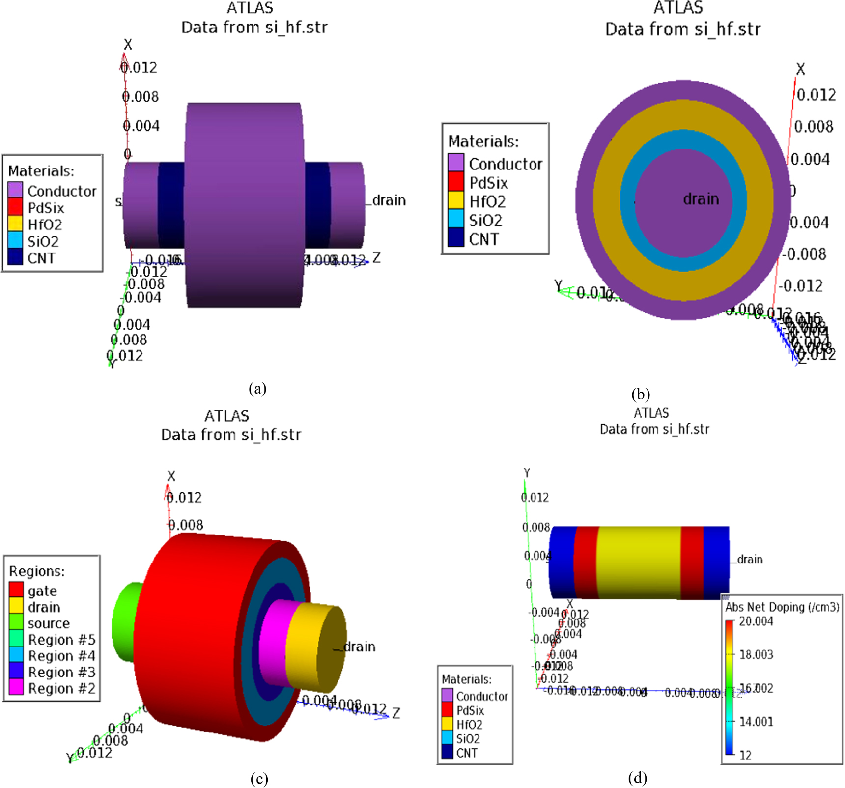
Figure 2 shows the geometry of GAA CNTFET modeled by Silvaco's ATLAS 3D tool, which uses a single CNT as a channel with gate wrapped around the channel to provide complete control over the flow of charge carriers through the channel as ballistic transport. The High_K gate dielectric materials have been used in CMOS process and FinFETs [24–26], the same concept of equivalent oxide thickness is used here to overcome gate tunneling which causes leakage through the dielectric layer and palladium as gate and source/drain contact materials due to its better wettability and compatibility with other material layers in the CNTFET device structure [13, 27]. The palladium as conductor for source/drain/gate contacts, heavily doped source/drain n+- regions with donor concentration of 1e + 20 /cm3 for ohmic contacts and SiO2-HfO2 stack as gate dielectric material to provide better gate coupling without increase in gate tunneling current for optimum device performance and leakage reduction has been used to model and simulate GAA CNTFET for robust applications.

Figure 2. Cylindrical (θ = 3600) GAA CNTFET modeled by Silvaco's ATLAS 3D, with CNT as channel, SiO2-HfO2 stack as gate dielectric, Palladium as gate and source/drain contact material, (a) GAA-CNTFET device structure , (b) Side View of GAA-CNTFET device structure, (c) Various regions of device, (d) Doping of various regions of the device; Heavily doped source/drain n+- regions with donor concentration of 1e + 20 /cm3 and lightly doped channel region of cylindrical GAA CNTFET device.
Download figure:
Standard image High-resolution image4. Device simulation and results analysis
This research investigates the semiconducting carbon nanotube and its use as a device channel in GAA CNTFET. The quantum confinement of carriers and current flowing in semiconductor devices have been modeled and simulated by Silvaco's device simulator. In semiconductor, the quantum confinement can be accurately calculated by Schrodinger-Poisson (SP) solver but this approach cannot predict the current flowing in the semiconductor devices. The Density Gradient (DG) modeling approach can be used to predict both the quantum confinement and the drift-diffusion currents along with the Fermi–Dirac statistics for 2D geometries. The Density Gradient (DG) modeling approach has limitations with 3D geometries and hence the Bohm Quantum Potential (BQP) modeling approach has been used for silicon/non-silicon, planar/non planar 3D structures [28, 29].
The Drift-Diffusion (D-D) is the simplest model of charge transport through semiconductor material and devices. The D-D model was adequate for the most of the semiconductor devices that were feasible by industry process standard. However, the D-D approach becomes less accurate for short channel devices. Therefore, the more advanced models are becoming popular for modeling and simulation of deep submicron devices. The Silvaco's ATLAS TCAD tool incorporates both the drift-diffusion and advanced transport models. The current equations in the drift-diffusion (D-D) model are given as [29, 30]:


where q is electron charge, is wave function, is the Boltzmann's constant, is lattice temperature, is effective intrinsic concentration and Dn, n, μn and, Dp, p, μp, are the diffusion coefficient, carrier concentration and mobility of electrons and holes respectively.
The quantum effects are included in Silvaco's ATLAS TCAD tool by changing the transport model equations with the position dependent Bohm quantum Potential (BQP). In Bohm Quantum Potential (BQP) model, the current equations (4) and (5) take the form as given [30]:


In equations (6) and (7) the additional term Q represents the Bohm Quantum Potential which is expressed as [29, 31]:

where is the reduced Plank's constant or Dirac constant, M is effective mass tensor, n is carrier concentration (electrons/holes), γ and α are two fitting parameters. We can calibrate and set the fitting parameter values γ and α along with the direction of the quantum confinement. Here, in this research, we have set values of γ and α as 1.4 and 0.3 respectively for device simulation.
This BQP model has several capabilities and advantages over other modeling approaches [29, 31, 32]. First, this model can be used not only for 1D structure but for 2D and 3D device structures as well. Second, it is numerically stable and does not depend on the transport models (drift-diffusion or hydrodynamic) used, and finally it exhibits better convergence properties. As the BQP model is available in the Silvaco's ATLAS TCAD tool, so we have used this BQP approach along with novel DFT based parameter estimation technique using MedeA VASP tool for modeling and simulation of GAA CNTFET device for sub nano scale applications.
4.1. The I-V characteristics of GAA CNTFET device
The device I-V characteristics of the modeled device have been analyzed and the performance parameters viz. VTH, SS, DIBL, ION/IOFF ratio etc extracted for investigations and optimization of the device behavior.
The input (ID-VGS) and output (ID-VDS) characteristics of gate all around CNTFET device in figure 2, are illustrated in figure 3. The input characteristics shows increase in current at VGS = 0.25 V to VGS = 0.8 V. The device operating at voltage VDS = 0.6 V gives drain current 4.75e-03A, at voltage VDS = VDD = 0.8 V gives drain current 1.45e-02A and high ION/ IOFF ratio and superior performance over bulk silicon and FinFET devices.

Figure 3. Input and output characteristics of cylinderical GAA CNTFET device. (a) Input charatceristics ID versus VGS at VDD = 0.6 V (b) Logrithmic: Input charatceristics log ID versus VGS at VDD = 0.6 V (c) Output charatceristics ID versus VDS at different gate volates (VGS); cnt_pd_1 = 0.2 V, cnt_pd _2 = 0.3 V, cnt_pd _3 = 0.4 V, cnt_pd _4 = 0.5 V, cnt_pd_5 = 0.6 V, VDS = (0–0.6 V) (d) Logrithmic: Output charatceristics log ID versus VDS at different gate volates (VGS); cnt_pd_1 = 0.2 V, cnt_pd _2 = 0.3 V, cnt_pd _3 = 0.4 V, cnt_pd _4 = 0.5 V, cnt_pd_5 = 0.6 V, VDS = (0–0.6 V), (e) Input charatceristics ID versus VGS at VDD = 0.8 V (f) Output charatceristics ID versus VDS at different gate volates (VGS); cnt_pd_1 = 0.2 V, cnt_pd _2 = 0.3 V, cnt_pd _3 = 0.4 V, cnt_pd _4 = 0.5 V, cnt_pd_5 = 0.6 V, cnt_pd_5 = 0.8 V, VDS = (0–0.8 V).
Download figure:
Standard image High-resolution image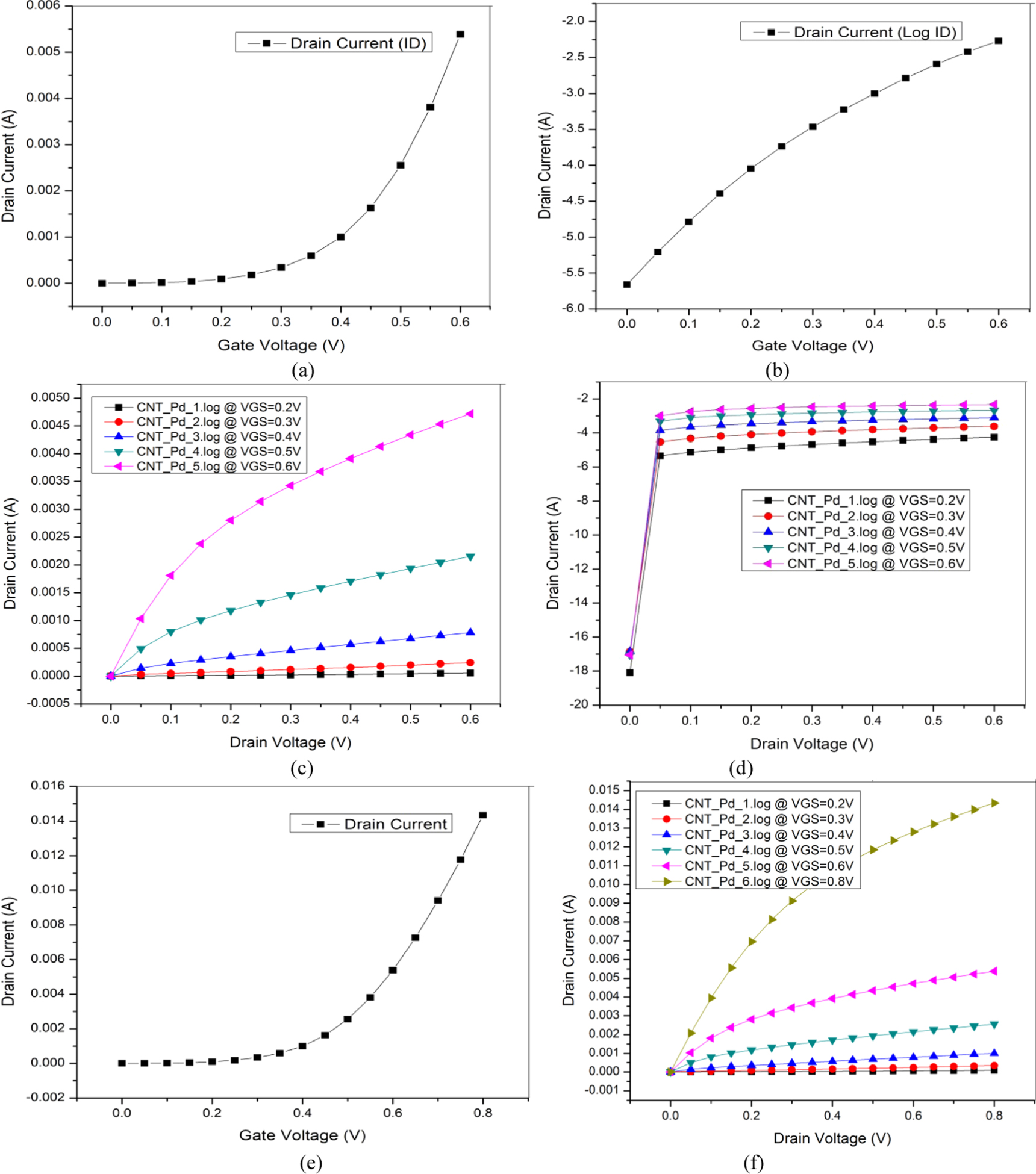
The performance comparison has been made with the published work of modeling, simulation and fabricated CNTFET devices with comparable device dimensions. The CNTFET devices have been promoted for years to replace silicon MOSFETs processing technology for low power and high performance sub nano scale applications as reported [6, 13, 34–36]. The results of our study have been compared with the experimental result of CNTFET using stacked high_k gate dielectric and Palladium as contact material with surround gate structure [13]. The device I-V characteristics of a self-aligned GAA-CNTFET exhibits a threshold voltage (Vth ) of 0.25 V and superb Ion/Ioff ratio >104 and a subthreshold swing (SS) of 99 mV/decade [13].
The performance parameters of the modeled-simulated and investigated devices of this research and from literature are summarized in table 3. The various comparative measures show that CNTFETs with surround gate geometry are better alternative to future semiconductor industry to meet various scaling, power and performance optimization targets.
Table 3. Comparative results of various performance parameters of CNTFET and FinFET devices.
| Device | |||
|---|---|---|---|
| Parameters | GAA CNTFET [This work] | GAA CNTFET [References] | FinFET [References] |
| Supply Voltage (VDD) | 0.8 V | 0.75 V [18], 1.0 V [13] | 0.8 V [11], 0.75 V [18] |
| Threshold voltage (VTH) | 0.254 V | 0.25 V [13] | 0.27 V [18] |
| Subthreshold Swing (SS) | 63.29 mV/dec | 67 mV/dec [18], 99 mV/dec [13] | 79 mV/dec [18] |
| ION/ IOFF ratio | 7.17e + 06 | 1.6e + 04 [18], 2.27e + 06 [10], >104 [13] | 2.5e + 03 [18], 4.24e + 05 [10] |
5. Conclusion
Keeping the miniaturization needs and performance improvement goals GAA CNTFET structure was simulated. The parameters required in the simulation of the CNTFET structure in Silvaco TCAD were obtained from the DFT based simulator MedeA VASP tool. The semiconductor devices using the GAA structure exhibit better ION/IOFF ratio, lower sub-threshold swing and increased threshold voltage, which further minimizes the sub threshold leakage and offer robust device performance. The GAA CNTFET device at supply voltage (VDD) 0.8 V exhibits threshold voltage (VTH) 0.254 V, sub-threshold swing (SS) 63.29 mV/dec, drain induced barrier lowering (DIBL) 72 mV/V and ION/ IOFF ratio 7.17e + 06. The GAA CNTFET device is robust for high performance nano scale applications. The results point towards the usage of CNT based GAA structure utility below 15 nm to further delay the death of Moore's law.
Acknowledgments
This work has been carried out at Nano materials Research Lab and VLSI Design Lab, Department of Electronic Science, Kurukshetra University Kurukshetra-136119. The first author is grateful to World Bank TEQIP and National Project Implementation Unit (NPIU)-India for providing research assistance ship.