
Abstract
The hole transport material (HTM)-free perovskite solar cells (PSCs) have attracted widespread interest due to enhanced stability and lowered cost as compared to the sandwich-type PSCs with an organic hole conductor. For the absorber layer, CsPbI3 has become a competitive candidate for its good chemical-components stability, excellent optoelectronic properties and most proper bandgap among inorganic halide perovskites. However, the power conversion efficiency of CsPbI3-based HTM-free PSCs is still much inferior to that of conventional ones. In this work, an all-inorganic-perovskite-heterojunction CsPbI3/CsSnI3 is proposed as the absorber and the HTM-free CsPbI3/CsSnI3 PSCs are investigated systematically through numerical simulation by using SCAPS-1D. Compared with the HTM-free PSCs employing a single CsPbI3 absorbing layer, the HTM-free CsPbI3/CsSnI3 PSCs have the extended absorption range and enhanced performance. The best cell efficiency is increased from 15.60% to 19.99% and from 13.87% to 19.59% for the cell with a back-front Au electrode and a back-front C electrode, respectively. It reveals that for the HTM-free CsPbI3/CsSnI3 heterojunction cells, C is a good choice for back-front electrode as it can achieve desirable cell performance with improved stability and lowered fabrication cost. These results indicate that the proposed HTM-free CsPbI3/CsSnI3 heterojunction cells are promising for photovoltaic applications.
Export citation and abstract BibTeX RIS

Original content from this work may be used under the terms of the Creative Commons Attribution 4.0 licence. Any further distribution of this work must maintain attribution to the author(s) and the title of the work, journal citation and DOI.
1. Introduction
Perovskite solar cells (PSCs) have been a focus in photovoltaic community owing to low fabrication cost and high efficiency. The certified power conversion efficiency (PCE) of the single-junction PSC has increased from 3.81% to 25.5% [1, 2]. The outstanding performance benefits from the excellent optoelectronic properties of halide perovskites, including suitable values of bandgap, strong absorption coefficient, high carrier mobility and long carrier diffusion length.
Most high-performance PSCs are based on hybrid organic-inorganic perovskites. Despite high efficiency, due to volatile and gyroscopic organic cation, hybrid organic-inorganic PSCs suffer from stability issues when exposed to moisture, illumination and raised temperature [3–5]. One method to improve stability of PSCs is to replace the organic cations with inorganic ones. Inorganic perovskite cesium lead halides CsPbX3 (X = Cl, Br, I, or mixed halogens) have demonstrated improved stability against moisture and high temperatures of up to 400 °C [6–8]. Due to a suitable bandgap and good tolerance to humidity, oxygen and thermal stress, CsPbI3 shows great prospect for stable PSCs. The CsPbI3 solar cell has been a rapid growing research field and impressive progresses have been made [9–12]. Many strategies have been developed to fabricate thermodynamically stabilized CsPbI3 solar cell and to improve cell efficiency. CsPbI3 solar cells with PCE over 19% have been reported by several groups [10–12].
The stability of PSCs is limited by not only the perovskite material but also the carrier transport material and the electrode. Most high-performance PSCs employ the expensive Spiro-OMeTAD as the hole transport material (HTM). This is unfavorable for mass production. Many reports indicate that Spiro-OMeTAD also has stability issue [13, 14]. Thanks to the bipolar transport characteristic of perovskite materials [15], PSCs can work without HTM. Removing of HTM can simplify the architecture of PSCs and is a possible way to solve the instability caused by HTM. The pioneer work of HTM-free PSCs was conducted by Etgar et al [16]. Up to now, the highest efficiency of single-junction HTM-free CsPbI3 solar cell is ∼14.6% [17], which is still much inferior to that of conventional ones. It is important to reveal the factors that limit the efficiency of HTM-free CsPbI3 solar cells and to find ways to improve their performance.
In this work, a HTM-free solar cell with the CsPbI3/CsSnI3 heterojunction as light absorbing layer is proposed and systematically studied via numerically simulation. The effects of absorber thickness, defect density of absorber, work function of electrode and doping level in absorber are investigated. It is found that incorporation of a CsSnI3 layer can greatly improve the efficiency of HTM-free CsPbI3 solar cells. Based on simulation, suggestions to enhance the performance of the HTM-free CsPbI3 solar cells are put forward.
2. Methodology
The device simulation was carried out by using SCAPS-1D software [18], a one-dimensional solar cell simulation program developed by the Department of Electronics and Information of Ghent University in Belgium. It is one of the well-known applications for simulation of solar cells and has been adopted in many studies for the modeling and simulation of perovskite solar cells [19–21]. SCAPS-1D simulates the internal carriers transport of solar cell by calculating coupled Poisson equation, continuity equations and constitutive equations. The complete set of equations is the following:
Where  is the vacuum permittivity,
  is the relative permittivity,
  is the electrostatic potential,
  is the electron charge,
  is the density of free electron and
  is the density of free hole.
  and
and  denote the ionized donor-like doping density, the ionized acceptor-like doping density, the trapped hole density and the trapped electron density, respectively. G is the optical generation rate,
  is the electron recombination rate,
  is the hole recombination rate.
  and
and  are the electron current density and hole current density, respectively.
  and
and  are used to account for the mobility of electron and hole, respectively.
  and
and  represent the quasi Fermi energy level of electron and hole, respectively.
The parameters employed in the simulations are shown in table 1 [22–27]. Taking into account the high recombination rate at interfaces, the TiO2/CsPbI3 and CsPbI3/C(Au) interfaces were inserted by an absorber layer (IDL1 and IDL2) with a thickness of 5 nm. The parameters of IDL1 and IDL2 are the same as the absorber except with a high-level defect density Nt of 1018 cm−3. The defect density of CsPbI3 absorber is set as 2 × 1014 cm−3 except for studying the influences of the defect density, where it varies from 1013 cm−3 to 1018 cm−3. The work function of the front contact is 4.1 eV (FTO). The following parameters are set to be identical for all layers. The defect energy level is at the center of bandgap and the defect type is neutral. Its energetic distribution is Gaussian with a characteristic energy of 0.1 eV. The absorption coefficient α is calculated using α = Aα (hν−Eg )1/2, where the absorption constant Aα is set as 105. The thermal velocity of electron and hole is 107 cm/s. Capture cross section of electron and hole is 2 × 1014 cm2.
Table 1. Material parameters used in simulation.
| Material properties | FTO [23] | TiO2 [24] | IDL1/ IDL2 | CsPbI3 [25, 26] | Spiro-OMeTAD [27] | CsSnI3 [22] |
|---|---|---|---|---|---|---|
| Thickness(nm) | 100 | 50 | 5 | 100–1000 | 170 | 0–1000 |
| NA(cm−3) | 0 | 4 × 10¹⁵ | 4 × 10¹⁵ | 1015–1020 | 2 × 10¹⁸ | 1020 |
| ND(cm−3) | 2 × 10¹⁹ | 1019 | 0 | 0 | 0 | 0 |

| 9 | 9 | 6 | 6 | 3 | 9.93 |
| χ (eV) | 4 | 4 | 3.95 | 3.95 | 2.45 | 3.6 |
| Eg (eV) | 3.5 | 3.2 | 1.73 | 1.73 | 3 | 1.3 |
 (cm2/V s)−1 (cm2/V s)−1
| 20 | 20 | 16 | 16 | 2 × 10⁻⁴ | 585 |
 (cm2/V s)−1 (cm2/V s)−1
| 10 | 10 | 16 | 16 | 2 × 10⁻⁴ | 585 |
| Nt (cm−3) | 1015 | 1015 | 1018 | 1013–1018 | 1015 | 1017,1018 |
| NC (cm−3) | 2.2 × 10¹⁸ | 1021 | 1.1 × 10²⁰ | 1.1 × 10²⁰ | 2.2 × 10¹⁸ | 1019 |
| NV (cm−3) | 1.8 × 10¹⁹ | 2 × 10²⁰ | 8 × 10¹⁹ | 8 × 10¹⁹ | 1.8 × 10¹⁹ | 1018 |
3. Results and discussion
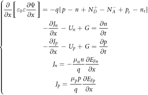
Figure 1 depicts the schematic device configuration of FTO/TiO2/CsPbI3/C PSCs and figures 2(a)–(d) show the simulated performance as a function of CsPbI3 thicknesses. For comparison, the results of corresponding cells with a Spiro-OMeTAD layer are also displayed. For both cells, the short circuit current JSC increases with the increase of absorber thickness. This is because a thicker perovskite layer absorbs more sunlight and produces more photocarriers. As CsPbI3 has a large absorption coefficient, a thickness of ∼1000 nm can absorb most incident sunlight and consequently JSC would saturate with such a thickness. As shown in figure 2(e), in the HTM-free solar cell, the absence of HTM causes a downward bend of energy band of CsPbI3 near the back-front (BF) electrode and thus results in a poorer collection of photocarriers and a smaller JSC . Compared with the HTM-containing counterpart, the HTM-free cell has a much smaller open circuit voltage VOC . This is due to the significant lowering of built-in barrier height in the HTM-free cell, as shown in figures 2(e) and (f). The built-in barrier height in the Spiro-OMeTAD-containing cell is mainly determined by difference in Fermi level between TiO2 and Spiro-OMeTAD. As a result, for the cell with a Spiro-OMeTAD layer, VOC depends weakly on CsPbI3 thicknesses. For the HTM-free cell, the built-in barrier height depends on the thickness of CsPbI3 and VOC increases with the increases of absorber thickness, first dramatically and then slowly. Removing the Spiro-OMeTAD layer increases the fill factor FF slightly. The smaller FF in the cell with a Spiro-OMeTAD layer is due to the low mobility of Spiro-OMeTAD. This is verified through controlled simulation (not shown here). In the cell with a Spiro-OMeTAD layer, with the increases of absorber thickness, FF decreases slightly. In the HTM-free cell, when the absorber thickness increases, FF first decreases and then increases. In general, the fill factor depends on VOC and various parameters that change the shape of current-voltage curves. For the present HTM-free cell, the changes of FF seems to correlate with that of VOC . FF decreases when VOC increases dramatically and increases when VOC increases slowly. Overall, removing the Spiro-OMeTAD layer increases FF slightly but lowers JSC , VOC and PCE remarkably. The increase of barrier height is important to promote the cell efficiency in the HTM-free cell.

Figure 1. Schematic structure of FTO/TiO2/CsPbI3/C cell.
Download figure:
Standard image High-resolution image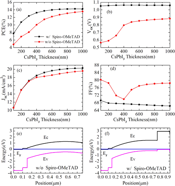
Figure 2. Effects of CsPbI3 thickness on (a) PCE, (b) Voc, (c) Jsc and (d) FF of FTO/TiO2/CsPbI3/C and FTO/TiO2/CsPbI3/Spiro-OMeTAD/C cells and energy band diagrams (in dark) for (e) FTO/TiO2/CsPbI3(600 nm)/C and (f) FTO/TiO2/CsPbI3(600 nm)/Spiro-OMeTAD/C. The hole doping level of CsPbI3 is 4 × 1015cm−3 and the defect concentration of CsPbI3 is 2 × 1014cm−3. In energy band diagrams, EF denotes the Fermi energy level, EC denotes the bottom of conduction band and EV denotes the top of conduction band.
Download figure:
Standard image High-resolution imageDefects in solar cells act as the recombination center and have significant influences of cell performance. Figure 3 shows the effects of defect density within CsPbI3 layers Nt (CsPbI3) on PCE, VOC , JSC , and FF of cells with Au or C as the BF electrode. For cells with these two electrodes, the variation trend is similar. When Nt (CsPbI3) is increased from 1013 to 1015 cm−3, PCE, Voc and Jsc decrease slowly. However, when Nt (CsPbI3) is larger than 1015 cm−3, PCE, Jsc and FF exhibit a significant decline. To achieve a high performance, it is essential to keep Nt (CsPbI3) lower than 1015 cm−3. In the following studies, Nt within CsPbI3 absorber is kept to be 2 × 1014 cm−3 .

Figure 3. Effects of defect density in CsPbI3 on (a) PCE, (b) Voc, (c) Jsc, and (d) FF for the FTO/TiO2/CsPbI3(350 nm)/C cell. The hole doping concentration of CsPbI3 is 4 × 1015cm−3.
Download figure:
Standard image High-resolution imageIn the HTM-free cell, the BF electrode contacts the absorber layer directly, causing a depletion region near the interface. Consequently, its work function influences the total barrier height and the cell performance. Figure 4(a) shows the J-V curves of the devices using BF electrodes with various work functions. When the work function is increased from 4.7 to 5.6 eV, both Jsc and Voc increase monotonically. It is notable that Voc increases from ∼0.43 V to ∼0.93 V as work function changes from 4.7 to 5.2 eV. In this range, with other parameters identical, the difference in Voc is exactly that in the work function of the BF electrode. As the work function approaches the top of valence band of CsPbI3, the increase in Voc becomes slower. Such an increase of Voc with increasing work function of BF electrode is related to the rise of barrier height, as shown in figure 4(b). A larger work function of BF electrode means a larger difference in Fermi energy between BF electrode and the absorber layer and results in a larger built-in potential. Tuning the work function of BF electrode could effectively improve the cell performance of HTM-free cell. As Au and C with a work function of 5.1 eV and 5.0 eV are commonly used as the BF electrodes for perovskite solar cells, comparative studies between C and Au electrodes are performed in this work.
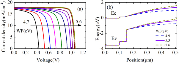
Figure 4. Effects of work function of back-front electrode on (a) J-V curves and (b) energy band diagram (in dark) for FTO/TiO2/CsPbI3(350 nm)/electrode cells. The hole doping level of CsPbI3 is 4 × 1015cm−3 and the defect concentration of CsPbI3 is 2 × 1014cm−3. In energy band diagram, EC denotes the bottom of conduction band and EV denotes the top of conduction band.
Download figure:
Standard image High-resolution imageThe doping level of CsPbI3 affects its Fermi level and the final built-in potential in the cell. Figure 5(a) shows J-V curves of FTO/TiO2/CsPbI3/C cells with different hole doping levels of CsPbI3 NA (CsPbI3). With the increase of NA (CsPbI3), JSC and VOC exhibit an oppsite trend. In short, JSC decreases and VOC increases, first quickly and then slowly. As a result, for cells with both electrodes, PCE first increases and then decreases, as shown in figure 5(b). A moderate hole doping in CsPbI3 can improve the performace of HTM-free CsPbI3 solar cell. The increase of NA (CsPbI3) shifts the Fermi level downwards and increases the difference in Fermi level between TiO2 and CsPbI3. As a result, the barrier height formed between TiO2 and CsPbI3 increases, causing an increase of VOC . Due to the increase of NA (CsPbI3) and the downward shift of Fermi level in CsPbI3, the depletion region in CsPbI3 becomes narrower and there is a downward bending of CsPbI3 energy band at CsPbI3/electrode interface (see figures 5(c) and (d)), which are harmful to the tranport and collection of photo-generated carriers and are responsible for the reduction of JSC .

Figure 5. (a) Effects of hole doping concentration in the CsPbI3 on illuminated J-V curves of FTO/TiO2/CsPbI3(350 nm)/C cells; (b) PCE as a function of hole doping concentration of FTO/TiO2/CsPbI3(350 nm)/C and FTO/TiO2/CsPbI3(350 nm)/Au cells; Energy band diagrams (in dark) of FTO/TiO2/CsPbI3(350 nm)/Au cells with a NA (CsPbI3) of (c) 1015cm−3 and (d) 1017cm−3 in CsPbI3. In energy band diagrams, EF denotes the Fermi energy level, EV denotes the bottom of conduction band and Ev denotes the top of conduction band.
Download figure:
Standard image High-resolution imageThe best values of PCE for FTO/TiO2/CsPbI3/C and FTO/TiO2/CsPbI3/Au cells with different NA (CsPbI3) after absorber thickness optimization are listed in table 2. All FTO/TiO2/CsPbI3/Au cells have a better cell performance than corresponding FTO/TiO2/CsPbI3/C cells. The best PCE is ∼15.60%, achieved in a cell with an Au electrode and a NA (CsPbI3) of 1016 cm−3. Due to the insufficient utilization of solar spectrum, this value is much inferior to that of hybrid organic-inorganic counterparts. With a relatively large bandgap (∼1.72 eV), sun light with a wavelength larger than 720 nm cannot be absorbed in CsPbI3. Such a loss may be reduced by combing CsPbI3 with another semiconductor with a smaller bandgap, such as CsSnI3 (bandgap ∼1.3 eV). Inorganic lead-free CsSnI3 has a high mobility and a high absorption coefficient [22, 28]. A critical issue of CsSnI3 is the oxidization of Sn2+ through self-doping reaction. Various efforts have been paid to solve this issue. Through additive engineering, it has been possible to achieve ambient-air stability for several days [29]. As CsSnI3 and CsPbI3 have the similar perovskite structure, it is possible to construct a CsSnI3/CsPbI3 heterojunction as the absorption layer in a HTM-free solar cell. Figures 6(a) and (b) show the schematic device structure of the HTM-free CsSnI3/CsPbI3 heterojunction solar cell and its energy band diagram. As shown, the incorporation of CsSnI3 could also facilitate the separation and transport of photo-generated carriers.
Table 2. Best cell performance for different cells obtained by absorber thickness optimization.
| Cell structure | Nt in CsSnI3 (cm−3) | NA in CsPbI3 (cm−3) | PCE (%) | Voc (V) | Jsc (mA cm−2) | FF (%) |
|---|---|---|---|---|---|---|
| FTO/TiO2/CsPbI3/Au | / | 1015 | 14.43 | 0.911 | 20.03 | 79.12 |
| FTO/TiO2/CsPbI3/Au | / | 1016 | 15.60 | 1.016 | 19.26 | 79.73 |
| FTO/TiO2/CsPbI3/Au | / | 1017 | 15.27 | 1.033 | 18.07 | 81.74 |
| FTO/TiO2/CsPbI3/C | / | 1015 | 12.62 | 0.811 | 19.95 | 78.01 |
| FTO/TiO2/CsPbI3/C | / | 1016 | 13.87 | 0.921 | 19.20 | 78.49 |
| FTO/TiO2/CsPbI3/C | / | 1017 | 13.65 | 0.957 | 18.03 | 79.13 |
| FTO/TiO2/CsPbI3/CsSnI3/Au | 1017 | 1015 | 19.99 | 0.959 | 26.59 | 78.41 |
| FTO/TiO2/CsPbI3/CsSnI3/Au | 1017 | 1016 | 19.85 | 0.964 | 25.56 | 80.59 |
| FTO/TiO2/CsPbI3/CsSnI3/Au | 1017 | 1017 | 18.28 | 0.953 | 25.50 | 75.18 |
| FTO/TiO2/CsPbI3/CsSnI3/C | 1017 | 1015 | 19.59 | 0.953 | 26.09 | 78.74 |
| FTO/TiO2/CsPbI3/CsSnI3/C | 1017 | 1016 | 19.29 | 0.958 | 24.89 | 80.84 |
| FTO/TiO2/CsPbI3/CsSnI3/C | 1017 | 1017 | 17.68 | 0.948 | 24.82 | 75.13 |
| FTO/TiO2/CsPbI3/CsSnI3/Au | 1018 | 1015 | 15.67 | 0.915 | 21.80 | 78.56 |
| FTO/TiO2/CsPbI3/CsSnI3/Au | 1018 | 1016 | 15.53 | 0.914 | 21.88 | 77.65 |
| FTO/TiO2/CsPbI3/CsSnI3/Au | 1018 | 1017 | 13.46 | 0.918 | 18.73 | 78.31 |
| FTO/TiO2/CsPbI3/CsSnI3/C | 1018 | 1015 | 15.62 | 0.915 | 21.74 | 78.56 |
| FTO/TiO2/CsPbI3/CsSnI3/C | 1018 | 1016 | 15.49 | 0.914 | 21.82 | 77.66 |
| FTO/TiO2/CsPbI3/CsSnI3/C | 1018 | 1017 | 13.42 | 0.917 | 18.69 | 78.32 |
Figure 6. (a) Schematic device configuration of the HTM-free CsSnI3/CsPbI3 heterojunction solar cell and (b) its schematic energy level diagram.
Download figure:
Standard image High-resolution imageFigure 7 displays the comparison of the J-V curves and quantum efficiency curves of two HTM-free solar cells using different light absorbing layers, CsPbI3(350 nm) and CsPbI3(350 nm)/CsSnI3(200 nm). The incorporation of a CsSnI3 layer improves JSC and VOC simultaneously. JSC is increased from 17.7 mA cm−2 to 22.2 mA cm−2 and VOC is increased from 0.73 V to 0.91 V. Correspondingly, PCE is increased from ∼8.9% to ∼15.5%. It is noted that JSC , VOC and PCE of FTO/TiO2/CsPbI3(1000 nm)/C cell are 19.6 mA cm−2, 0.88 V and 13.6%, respectively. These values are all smaller than the corresponding performance parameters of the FTO/TiO2/CsPbI3(350 nm)/CsSnI3(200 nm)/C cell. The increase of JSC in FTO/TiO2/CsPbI3/CsSnI3/C cell is partly due to the increase of absorber thickness and partly due to the extension of the absorption spectrum to the near infrared region. As shown in figure 7(b), the quantum efficiency of FTO/TiO2/CsPbI3/C reaches a maximum value in the wavelength range of 360–440 nm and drops near 720 nm, above which no light is absorbed. The incorporation of CsSnI3 not only increases the quantum efficiency below 720 nm but also extends the absorption range to the infrared region. The increase of VOC in FTO/TiO2/CsPbI3/CsSnI3/C cell is due to combined effects. Voc could be expressed as VOC = nkB T/qln(JL /J0 + 1), where n is the ideality factor, kB is the Boltzmann constant, T is the temperature, q is the electric charge, JL is the photo-generated current density and J0 is the dark saturation current density. With other parameters fixed, an increase of JL from 17.7 mA cm−2 to 22.2 mA cm−2 lead a small increase of VOC . By fitting the dark J-V curve with J = J0 exp(qV/nkB T), one can obtain the dark saturation current density J0 , which is 2.03 × 10⁻⁸ mA cm−2 for the CsPbI3 cell and 9.67 × 10⁻¹⁵ mA cm−2 for the CsPbI3/CsSnI3 cell. The calculated values of VOC_calc [=nkB T/q ln(JL /J0 + 1)] are 0.68V for the CsPbI3 cell and 0.90 V for the CsPbI3/CsSnI3 cell, which are in good accordance with the VOC (0.73 V and 0.91 V) obtained from the simulated J-V curves under illumination. Thus, the increase of VOC in FTO/TiO2/CsPbI3/CsSnI3/C cell is due to the combined effects of the increase of photocurrent and the decrease of dark saturation current density.
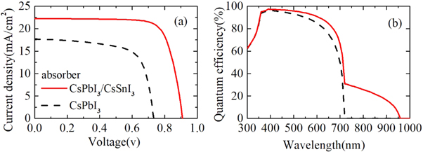
Figure 7. (a) Illuminated J-V curves and (b) quantum efficiency curves of the FTO/TiO2/CsPbI3(350 nm)/C and FTO/TiO2/CsPbI3(350 nm)/CsSnI3(200 nm)/C cells. The hole doping level of CsPbI3 is 4 × 1015cm−3 and the defect concentration of CsSnI3 is 1 × 1018cm−3.
Download figure:
Standard image High-resolution imageFigure 8 shows the current density distribution and quantum efficiency for the FTO/TiO2/CsPbI3/CsSnI3/C cells with different values of NA (CsPbI3) and Nt (CsSnI3). For a fixed Nt (CsSnI3), the increase of NA (CsPbI3) causes a decrease of quantum efficiency in the whole spectral range, especially for wavelength larger than 720 nm. From the distribution of current density, it is found that with an increase of NA (CsPbI3) the carrier transport between CsSnI3 and CsPbI3 is suppressed. As discussed in a previous section, with a higher hole doping concentration in CsPbI3, the energy band of CsPbI3 moves upward and there would be a downward bending of CsPbI3 energy band at the CsPbI3/CsSnI3 interface (similar to that shown in figure 5(d)), which would suppress the carrier transport between CsSnI3 and CsPbI3. Thus, a low hole doping concentration in CsPbI3 is beneficial for carrier transport in CsPbI3/CsSnI3 cells. With a fixed NA (CsPbI3), the increase of Nt (CsSnI3) decreases the quantum efficiency and the photo-current from CsSnI3. This is understandable as a higher defect concentration causes more recombination and less carrier collection.
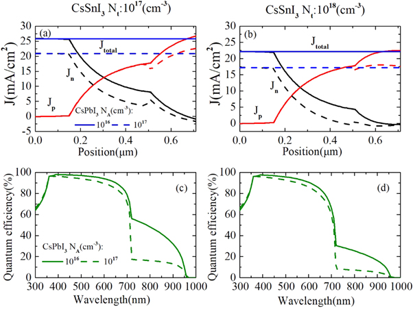
Figure 8. (a)(b) Current density distribution and (c)(d) quantum efficiency curves for the FTO/TiO2/CsPbI3(350 nm)/CsSnI3(200 nm)/C cells with different values of Nt (CsSnI3) (1017 and 1018cm−3) and NA (CsPbI3) (1016 and 1017cm−3).
Download figure:
Standard image High-resolution imageFigure 9 shows the absorber thickness optimization for the FTO/TiO2/CsPbI3/CsSnI3/Au cell with a NA (CsPbI3) of 1015 cm−3 and a Nt (CsSnI3) of 1017 cm−3. It can be found that with a fixed thickness of CsPbI3, with the increase of CsSnI3 thickness, JSC and VOC first increase dramatically and then show a saturation behavior. The maximum PCE is ∼19.99%, which occurs in a cell with the CsPbI3(200 nm)/CsSnI3(300 nm) as the absorbing layer. This efficiency is much larger than the maximum PCE obtained in the FTO/TiO2/CsPbI3/Au cell (14.43%) with an identical hole doping in CsPbI3. Moreover, a cell efficiency above 19% can be achieved with various thickness combinations.

Figure 9. Absorber thickness optimization for the FTO/TiO2/CsPbI3/CsSnI3/Au cell with a NA (CsPbI3) of 1015 cm−3 and a Nt (CsSnI3) of 1017 cm−3.
Download figure:
Standard image High-resolution image
Table 2 also summarizes the best cell performance for various FTO/TiO2/CsPbI3/CsSnI3/C and FTO/TiO2/CsPbI3/CsSnI3/Au cells obtained through absorber thickness optimization. The optimization process is similar as that displayed in figure 9. Three hole-doping levels in CsPbI3 (1015, 1016 and 1017 cm−3) are studied. As the defect concentration in the CsSnI3 films is usually quite high, the defect concentration in CsSnI3 is set to be 1018 cm−3 and 1017 cm−3.
In all CsPbI3/CsSnI3 cells, the best PCE depends on the hole concentration in CsPbI3. This is similar to that in cells with a single CsPbI3 absorbing layer, but the dependence is different. In cells with a single CsPbI3 absorbing layer, with the increase of NA (CsPbI3), the maximum PCE first increases and then decreases. The peak values of maximum PCE appears in the cell with a NA (CsPbI3) of 1016 cm−3. For FTO/TiO2/CsPbI3/C cell and FTO/TiO2/CsPbI3/Au cell, the peak value of maximum PCE is ∼13.87% and ∼15.60%, respectively. The cells with a CsPbI3/CsSnI3 absorbing layer show best performance at a NA (CsPbI3) of 1015 cm−3. An increase of NA (CsPbI3) to 1016 cm−3 cannot improve the cell performance. Instead, it causes a slight decrease of maximum PCE. A further increase of NA (CsPbI3) to 1017 cm−3 leads a much larger decrease of maximum PCE. As discussed above, a higher hole doping concentration in CsPbI3 suppresses the carrier transport between CsSnI3 and CsPbI3 and decreases JSC .
If NA in CsPbI3 is low, e.g. 1015 cm−3, even incorporation of a CsSnI3 absorbing layer with a Nt of 1018 cm−3 can improve the cell performance considerably. For the cell with a BF Au electrode, the maximum PCE is enhanced from 14.43% to 15.67%. This improvement is comparable to that due to the increase of NA (CsPbI3) for the cell with a single CsPbI3 absorbing layer. For the cell with a BF C electrode, the maximum PCE is enhanced more significantly, from 12.62% to 15.62%. This larger improvement originates from simultaneous enhancement of JSC and VOC . If NA (CsPbI3) is higher, the incorporation of a CsSnI3 absorbing layer with a Nt of 1018 cm−3 would lead a much smaller improvement and even a deterioration of cell performance.
If Nt in the incorporated CsSnI3 is reduced to 1017 cm−3, the incorporation of a CsSnI3 layer can significantly improve cell performance for all three values of NA (CsPbI3) and both BF electrodes. The FTO/TiO2/CsPbI3/CsSnI3/Au cell with a Nt (CsSnI3) of 1017 cm−3 shows a best PCE of 19.99%, 19.85% and 18.28% for a NA (CsPbI3) of 1015, 1016 and 1017 cm−3, respectively. For FTO/TiO2/CsPbI3/CsSnI3/C cell, the best PCE is 19.59%, 19.29% and 17.68% for a NA (CsPbI3) of 1015, 1016 and 1017 cm−3, respectively. These values of PCE are much larger than those in the counterpart cells with a single CsPbI3 absorbing layer. For all three NA (CsPbI3) levels and both BF electrodes, the incorporation of a CsSnI3 layer increases JSC significantly due to a better utilization of solar spectrum. For the cell with a low NA (CsPbI3), JSC and VOC could be enhanced simultaneously. As a result, the improvement of cell performance is most significant.
It is noted that for CsPbI3/CsSnI3 cells, the efficiency of the cell with a BF C electrode is comparable to that with a BF Au electrode. This is different from cells with a single CsPbI3 absorbing layer, where the efficiency of the cell with a BF Au electrode is considerably larger. It is also noted that the C electrodes are beneficial for improving the stability of PSCs, especially the HTM-free ones [30]. Thus, for the HTM-free CsPbI3/CsSnI3 heterojunction cells, C is a good choice for BF electrode as it can achieve desirable cell performance with improved stability and lowered fabrication cost.
4. Conclusion
In order to improve the cell performance of CsPbI3 based HTM-free PSCs, CsPbI3/CsSnI3 heterojunction was proposed as the absorber and HTM-free CsPbI3/CsSnI3 PSCs were investigated systematically through numerical simulation by using SCAPS-1D. In the HTM-free cell with a single CsPbI3 absorbing layer, though the cell performance can be improved through optimization of various parameters, e.g. absorber thickness, defect density of absorber, work function of electrode and doping level in absorber, its performance is greatly limited by the relatively large bandgap of CsPbI3. Incorporation a narrow-bandgap perovskite CsSnI3 in the cell extends the absorption spectrum and facilitate the separation and transport of photo-generated carriers. For the CsPbI3/CsSnI3 cell, it is beneficial to keep a low hole doing in CsPbI3. With a hole concentration of 1015 cm−3 in CsPbI3, even incorporation of a CsSnI3 layer with a defect concentration of 1018 cm−3 can improve the cell efficiency from 14.43% to 15.67% and from 12.62% to 15.62% for the cell with a back-front Au electrode and a back-front C electrode, respectively. If the defect concentration in the incorporated CsSnI3 is reduced to 1017 cm−3, the incorporation of a CsSnI3 layer can increase the cell efficiency to 19.99% and 19.59% for the cell with a back-front Au electrode and a back-front C electrode, respectively. For the HTM-free CsPbI3/CsSnI3 heterojunction cells, C is a good choice for back-front electrode as it can achieve desirable cell performance with improved stability and lowered fabrication cost. The stability of CsSnI3 has great impacts on the results. If the stability of CsSnI3 can be further enhanced, these results would provide a theoretical basis for fabrication of CsPbI3 based HTM-free PSCs.
Acknowledgments
This work was supported in part by the Zhejiang Provincial Natural Science Foundation of China under Grant LY19A040006, Grant LY21F010010 and Grant LY22A040002; in part by the National Natural Science Foundation of China under Grant 11504356 and Grant 51771175.
Data availability statement
All data that support the findings of this study are included within the article (and any supplementary files).
Conflicts of interest
There are no conflicts of interest to declare.