

Abstract
This article presents recent progress and a comprehensive overview of stretchable interconnects based on printable nanocomposites. Nanocomposite-based inks for printed stretchable interconnects have been categorized according to dispersed filler materials. They comprise of carbon-based fillers and metal-based fillers. Benefits in terms of excellent electrical performance and elastic properties make nanocomposites the ideal candidates for stretchable interconnect applications. Deeper analysis of nanocomposites-based stretchable interconnects includes the correlation between the size of fillers, percolation ratio, maximum electrical conductivity and mechanical elasticity. The key trends in the field have been highlighted using curve fitting methods on large data collected from the literature. Furthermore, a wide variety of applications for stretchable interconnects are presented.
Export citation and abstract BibTeX RIS

Original content from this work may be used under the terms of the Creative Commons Attribution 3.0 licence. Any further distribution of this work must maintain attribution to the author(s) and the title of the work, journal citation and DOI.
1. Introduction
Recent years have witnessed a paradigm shift in the electronics industry towards the development of flexible and stretchable electronics. Development of flexible and stretchable devices has enabled new pathways and interaction mechanisms for applications such as wearable electronics [1, 2], consumer electronics [3], electronic skin (E-skin) [4, 5] and robotics [6–8], etc. However, realization of such devices with traditional materials such as silicon is a challenge owing to their intrinsic properties such as brittleness that limit their ability to stretch or bend [9, 10]. Although recent studies on silicon micro/nanostructures [11–14] and ultra-thin chips [15, 16] have demonstrated the feasibility of silicon-based flexible electronics. In this regard, stretchable interconnects are interesting as they can provide traditional rigid electronic systems an extra degree of freedom while retaining the performance of original rigid devices. In applications such as electronic or tactile skin in robotics, the stretchability can improve conformability with various curved parts [10].
The field of stretchable electronics has been widely reviewed in terms of materials and applications. For example, Bao et al reviewed the development of stretchable electronics in context with e-skin [17, 18]. Rogers et al focused on various materials and geometries for stretchable electronics [19–21]. Many other reviews have focused on different geometries and the role of materials is not much covered [22, 23]. Materials such as rubber-like nanocomposites have been extensively reviewed by researchers in terms of their electrical properties, synthesis and fabrication technologies [24, 25], but their role in stretchable electronics has not been reviewed yet. This review article bridges this gap and extends the discussion on nanocomposites towards stretchable electronics. Furthermore, we also discuss the correlation between the electrical and mechanical properties of the rubber-like nanocomposite, which were not discussed before. This article presents a detailed discussion on printable nanocomposites that can be used as stretchable interconnects.
In terms of historical perspective, the need and interest for the development of flexible electronics can be traced back to the 1960s, as shown in figure 1. The need to capture solar energy in space application and the energy crisis of late 1960s were the motivating factors for research on flexible electronics [26]. The shift from rigid to flexible solar panels was driven by the benefits of flexible panels such as a larger active area, lighter weight and more resistance to thermal and vibration shocks [26]. New applications such as flexible ribbons/wires in computers led to further growth in the use of flexible electronics. More recently, applications such as robotics and soft robotics [27], prosthetics [28], implantable electrodes [1], and wearable systems [29] etc, have led to significant growth in the field of flexible electronics. This is evident from the exponential increase in the number of publications in this field in last fifteen years (figure 1). By incorporating a degree of flexibility, the performance of multifunctional electronic systems could be extended for various applications. However, applications where large deformation is experienced, it is imperative to have stretchability. As an example, large deformation is experienced at complex surfaces such as the knees and elbows of a humanoid robot where the need for tactile skin has been highlighted by many researchers [10, 28, 30, 31]. However, flexible electronics with such large deformations and similar performance as traditional silicon-based electronics is not there yet. For this reason, the stretchability of tactile skin with rigid electronic components connected via stretchable interconnects has been explored as a solution in such cases. Likewise, stretchable electronics with islands of rigid electronic chips on flexible substrates and connected with each other via stretchable interconnects has been explored for wearable and biomedical applications [1, 32–34]. The stretchability also improves conformability of electronics with the body and thus improves the reliability of the measurement of vital health parameters via wearable systems. New materials such as graphene could add a new dimension to this research through features such as transparency and high electrical conductivity [35]. These advances have also led to the exponential growth in the field of stretchable electronics, especially in the past decade, as can be seen from figure 1. It can be noted that the growth in stretchable electronics is expected to surpass that in flexible electronics. This is perhaps due to the increasing number of applications requiring stretchable electronics. In terms of the actual number of publications, flexible and stretchable electronics are expected to attract about 15 000 and 5600 papers, respectively, by the year 2020.
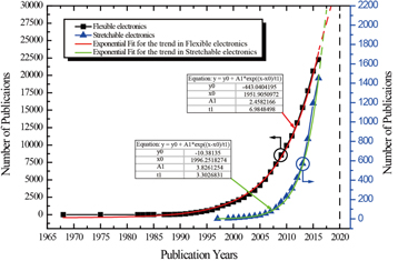
Figure 1. The trend from the accumulated number of publications during 1965 to 2020. The data was extracted from Web of science by searching keywords such as flexible electronics and stretchable electronics.
Download figure:
Standard image High-resolution imageThis article is structured as follows: section 2 gives a general overview of stretchable interconnects and various structural geometries and materials are briefly discussed. Since these topics have been reviewed in past, the discussion of these topics has been intentionally kept brief and covered to serve the purpose of presenting a complete story. Section 3 describes different printing technologies to fabricate stretchable interconnects. Section 4 presents various materials for printable interconnects with a particular focus on the electrical and mechanical properties of nanocomposites. Then, several applications of stretchable interconnects, including those based on nanocomposites and various geometries are presented in section 5. Section 6 summarizes the review with key observations and future research directions.
2. A general overview of stretchable interconnects
Generally, stretchable systems can be obtained in two ways: (a) engineered shapes, and (b) rubber-like materials that are intrinsically stretchable. Figure 2 summaries various types of methods for stretchable interconnects from these two categories along with the maximum possible elongation achieved for each of them. Engineered geometries such as helical wires have been widely used for stretchable interconnects for a long time. The idea of helical conductive wire is straightforward; it resembles the structure of a spring or wire connecting a telephone receiver to its base in recent years [36, 37]. The helical shape makes the wire stretchable (rather expandable) and allows the telephone receiver to be moved away from the base. While telephone wires have vanished, thanks to the advent of wireless technology, the techniques of stretchable wires have found new applications, such as in a stretchable tactile skin. Expandable spiral electrodes, obtained by winding the copper wires around an elastic nylon line, have been used to obtain large-area tactile skin [38]. Conductive thread-based clothing has been used in stretchable wearable electronics [39, 40]. Likewise, stretchable fabrics with knitted tactile sensing materials or tactile sensitive fabrics have been reported for stretchable tactile sensing [30, 41]. The fabrication of such stretchable systems often requires a core that can be chosen as the elastic thread. Then the conductive wire is wound around the core under a precise control in pitch and winding speed to build the helical shape. The wire can either be commercial copper wires [37] or elastic polymeric wires coated with highly conductive material (e.g. AgNW [36]). Depending on the winding pitch and wiring material, the failure strain of such designs can reach up to 100% with an increased resistance by 70% [36]. However, the large diameter of winding coil narrows the scalability of such geometries.

Figure 2. Various designs in engineered geometries of stretchable interconnect which are sorted according to their maximum elongations (stretchability) with respect to the scale of the structure size achieved by different patterning technologies.
Download figure:
Standard image High-resolution imageAnother engineering technique for obtaining stretchable structures involves realizing conducting layers in 'wavy' or serpentine shapes [42–45]. Compared to the limited scalability possible in helical coil and threads, the geometry of in-plane 'wavy' design and buckled film can be easily scaled down to the microscale by microfabrication technology (figure 2). With a careful design of its 'wavy' amplitude, the curvature and the width, the optimized structure can be applied up to 90% strain with a negligible influence on electrical response [45]. The out-of-the-plane 'wavy' structure or the buckled film can either be deposited along with the buckled substrate [46] or partial-free standing on the substrate [11, 47]. The stretchability of wavy structures on buckled substrates mainly relies on the degree of pre-straining of the substrate which is limited due to the substrate's stretchability, on the other hand, the interconnects that are partial-free stand on the substrate can have a higher degree of stretchability benefit from the releasing from the substrate scheme. In this way, the stress generated at the interface between the conducting film and soft substrate can be avoided and this allows the film to have a longer possible elongation. Another strategy for stretchable conductors is to fabricate net-shaped conductive structures by releasing a pre-strained elastic substrate with conductive materials lying on it. Taking advantage of this technique, different stretchable conductors, such as metal-coated net films, wavy one-dimensional metal ribbons or two-dimensional metal membranes have also been demonstrated [48].
Stretchability of interconnects can also be enhanced by engineering the topography of the substrate. One such example is implementing mini-valleys on the surface of a soft substrate followed by metal coating. This results in a structure with a stable electrical behavior over a repeatable cyclic stretching [49]. Other than implementing mini-valleys on the surface of the substrate, the honeycomb lattice architecture or sponge-like structure is designed by introducing vias or air pores to the substrate. The conductive sponge can either be achieved by electrodeless-plating on commercially available PU sponge [50] or carbon nanotube sponge [51]. Recent research on multilayer graphene sponge has also generated much interest [52]. However, the idea of using conductive sponge for stretchable interconnects has several limitations including the size of pores in the sponge, which decides both the minimum dimension of the interconnects and the stretchability of the interconnects. With smaller pore size the interconnect structure could be finer, but at the same time less stretchable. Further, there are challenges related to the integration and soldering of such structures as the pores in the structure do not allow seamless integration as in conventional electronics. Some technologies can realize a very fine structure of interconnects. For example, the nano-mesh structure fabricated by grain boundary lithography. This nanoscale structure can withstand strain up to 160%. However, after 1000 cycles' test, the resistance changed significantly [53]. Another example is the nano-accordion structure, which is made of Al doped ZnO. This structure can be elongated up to around 53%, but in the meantime the resistance changed dramatically [54].
A truly stretchable conductor should be like rubber—stretching and regaining the original shape after release, and ideally with negligible variation in the conductivity. Such interconnects are discussed in details in the following sections of this review. Few examples of this type of (non-ideal) stretchable conductor include elastic conductors based on Single-Walled Carbon Nano Tubes (SWNT)-PDMS composite films embedded in PDMS or coated with dimethylsiloxane-based rubber [55–58]. In these interconnects, the nanotubes carry the electricity and the rubber provides the stretchability. These conductors allow uniaxial and biaxial stretching of 70%–100%—without mechanical or electrical damage. The microfluidics approach is yet another interesting alternative that has been developed in recent years to obtain stretchable conductors. In this approach, the wires are replaced with conductive liquid confined in microfluidic channels [59]. These approaches are not yet at a stage where they can be employed in large area integration. Nonetheless, recent advances in material engineering, highlighted in this article, do raise hope.
3. Technologies for printed stretchable interconnects
Printing technologies are widely used for the development of flexible and stretchable electronics as they offer a cost-effective fabrication alternative to lithography-based approaches [60]. As illustrated in figure 3, these technologies encompass a number of methods including microcontact printing, transfer printing, spray coating, inkjet printing and screen printing [60]. An excellent overview of various printing technologies for flexible electronics is given in [60]. The technologies most relevant to stretchable interconnects are briefly described here. These printing techniques are preferred over other patterning techniques such as photolithography and electron beam lithography for the development of large area electronics applications owing to their low cost and fast processing speed, which make them attractive in terms of manufacturing [60]. The materials, which are compatible with printing technologies, range from conductors, dielectrics, and semiconductors in the form of dispersed solution, colloids and paste. The concept of printing technology is to spread and pattern the ink/paste directly on the substrate with the help of specific printing equipment. For instance, microcontact printing involves a pre-fabricated stamp gaining contact with the conductive ink first and this is followed by contact with the target substrate under specific pressure, as described in figure 3(a). The reported resolution can reach a line width of 314 μm with a space of 286 μm [61]. The stamp in the process can be repeatably used. However, with an overload contact pressure the stamp can easily pick up excessive ink, which affects the final resolution of the printed structures. More precise patterns with a minimum structure of up to 5 μm resolution can be achieved with the help of a Nanoimprint machine [62]. Another popular printing technology is spray coating (figure 3(c)). This technology utilizes a nozzle to spray solution-based materials on the substrate. Spray coating has the advantage of efficient material usage but the resolution can be poor. It is often used in combination with other printing technologies such as contact printing or transfer printing [63–66]. Compared to spray coating, inkjet printing can realize a versatile pattern directly from graphical designs (figure 3(d)). The achievable resolution by spray and inkjet printing is hugely dependent on parameters such as the diameter of the nozzle and the distance between the targeting substrate, etc [67, 68]. The limitation of the nozzle diameter restricts the size of the particle in the ink used for these printing technologies. In this regard, solution-based or colloid-based ink is preferred for homogeneous coating and the relevant printing technologies are called screen or stencil printing. Screen printing utilizes a paste-like ink which is more viscous compared to spray and inkjet printing. As shown in figure 3(e), the setup of screen printing comprises of a stencil, squeegee, a press bed and the substrate, The resolution is limited by the mesh size from the stencil, the viscosity of the ink, the surface energy of the substrate and the speed of printing etc [69, 70]. The viscosity of the ink has to be carefully controlled to avoid the over-spreading of printed ink and to control the printing resolution. Currently, the highest resolution of this technology is about 50 μm [71].

Figure 3. Printing technologies including (a) microcontact printing, (b) transfer printing, (c) spray coating, (d) inkjet printing, (e) screen printing.
Download figure:
Standard image High-resolution image4. Materials for printed stretchable interconnects
4.1. Intrinsic conductive and elastic interconnects
Traditionally, metals such as gold and copper have been preferred for interconnects and electrodes, owing to their high electrical and thermal conductivity that permits an influx of large current and fast transmission of signals. However, when it comes to stretchability the metals have been found to have limited use as they are not elastic enough [46, 72]. For example, the metal interconnects exhibit an elastic modulus of about 100 GPa. On the other hand, highly stretchable elastomers such as PDMS and PU etc, which are often used as highly stretchable substrates, exhibit an elastic modulus below 1 MPa. For this reason, the use of metal for a stretchable interconnect application has been achieved through engineered geometries described in section 2. The stretchable interconnects that act like rubber, i.e. stretching and regaining the original shape after release, with negligible variation in the conductivity, offer an interesting alternative. These interconnects are based on various nanocomposites, which are made by mixing a variety of conducting filler materials in a matrix of soft and rubbery materials. A comparison of the elastic modulus and electrical conductivity of various insulating polymers, metal and carbon-based filler materials is given in figure 4. While mechanical stretchability and electrical conductivity are prerequisites for stretchable interconnects, the interaction between the conductor and polymer substrate is crucial as well. Huge differences in elastic modulus between the substrate and conducting materials can lead to a highly concentrated stress at the interface and thus can have unreliable operation [46]. In order to mitigate this effect, novel conductive materials that can balance the mechanical stretchability and electrical conductivity are in high demand. A few examples of intrinsic conductive and stretchable materials are presented in figure 5.
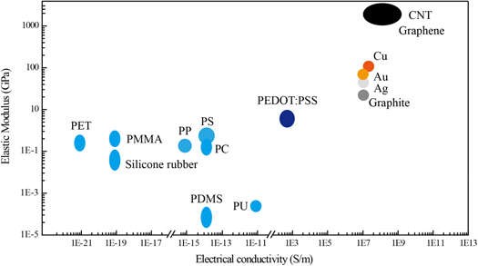
Figure 4. Comparison of the elastic property of various materials (including insulating polymers, organic conductive polymer, metals and carbon materials) for stretchable interconnects with electrical conductivity.
Download figure:
Standard image High-resolution image
Figure 5. (a) Flexible OPV based on PEDOT:PSS. Reprinted from [79], copyright 2011, with permission from Elsevier. (b) Liquid metal interconnected LED, [82] John Wiley & Sons. © 2013 WILEY-VCH Verlag GmbH & Co. KGaA, Weinheim. (c) Ionic Hydrogel-based stretchable electrode. From [80]. Reprinted with permission from AAAS. (d) Commercially available AgNW-based screen-print ink, [71] John Wiley & Sons. © 2016 WILEY-VCH Verlag GmbH & Co. KGaA, Weinheim. (e) Stretchable interconnects based on screen-printed silver paste. Reproduced from [84]. CC BY 4.0.
Download figure:
Standard image High-resolution imageOrganic conductive polymers have emerged as popular candidates for filler materials, owing to their acceptable electrical conductivity and mechanical softness [6]. Some of the widely used organic conductors include Polyaniline (PANi) [73] and Poly(3, 4-ethylenedioxythiophene): poly(4-styrenesulfonate) (PEDOT:PSS) [74]. They have modest electrical conductivity (∼100 S cm−1) and are soft enough for up to 10% stretching without any cracks in the film [74]. Furthermore, being transparent they can be used in optoelectronic device applications [75, 76]. The electrical conductivity of these conductive polymers is limited. In the case of PEDOT:PSS, the highly conductive PEDOT grains are surrounded by excess weakly ionic-conducting PSS. Although the PSS ions help PEDOT to be easily dispersed in water, it separates PEDOT from establishing a conductive path [77]. A secondary doping can improve the electrical conductivity of the resulting PEDOT:PSS film [75, 78] and the maximum conductivity can be in the order of 1000 S cm−1, which is still low in comparison with metals. An example of PEDOT:PSS, replacing ITO in solar cells is given in figure 5(a) [79].
Another type of filler material is the ionic-Hydrogel electrode, which is made of PAM-Aam (LiCl) and is highly elastic and electrically conductive [80]. The elastic modulus of ionic-hydrogel electrode filler material is lower than an elastomeric substrate such as Ecoflex. Therefore, the substrates deposited with ionic-hydrogel electrode do not show any phenomenon of delamination even when they are stretched up to 500%. Besides conductive polymers, liquid metals such as eutectic gallium-indium (EGaIn) incorporated within microchannels in an elastic polymeric substrate [81] are also investigated for stretchable interconnect applications. The use of EGaIn as stretchable interconnects to connect LEDs is shown in figure 5(b) [82]. Although they result in a reliable and robust interconnect system, the complexity associated with fabrication and encapsulation of microchannels in such structure limits their use. Another popular group of materials for stretchable interconnects is the conductive nanocomposite. These nanocomposites have highly conductive fillers dispersed within the elastic polymer matrix and their electrical conductivity can be tuned by varying the load volume of the filler material. The achieved electrical conductivity can reach up to the level of 106 S m−1 and the stretchability can be up to 100% [83]. A few examples of screen printed nanocomposites for stretchable interconnects are shown in figures 5(d)–(e) [71, 84]. The conductive nanocomposites show strong advantages over the organic polymer, ionic hydrogel and the liquid metal in terms of electrical conductivity and mechanical elasticity. This article is focused on a composite based on a variety of conductive fillers which is composed of metal-based fillers, carbon-based fillers and semi-conductor-based fillers. A detailed study of these materials is presented in the following section.
4.2. Nanocomposite-based stretchable electrode
Conductive nanocomposites benefit from the high electrical performance of fillers dispersed in the elastic polymer matrix. The synthesis of these nanocomposites with an appropriate mix of fillers in the polymer matrix is critical in terms of performance. The synthesis process requires three following essential elements: the conductive filler, the binder (polymer matrix) and the solvent [71]. To make sure the fillers are homogeneously dispersed in the matrix, an appropriate solvent is selected to de-bundle the fillers. Simultaneously, the sonication power and duration should be tuned to transduce the energy for dispersing the filler homogenously without breaking them [85]. In general, the electrical behavior will be enhanced if the loading ratio of fillers is increased. However, the elastic modulus of the resulting composite is also increased in the process and therefore a trade-off is needed between the elastic modulus and electrical conductivity. The following sub-sections describe the theory governing this trade-off and a comparison of various nanocomposites based on a variety of conductive fillers.
4.2.1. Percolation and tunneling theory
The conductivity of nanocomposites varies as a result of the variations in filler concentration [10]. The conductivity is governed by the percolation theory, which is represented by [60, 86]:

Where  is the bulk conductivity of the composite,
  is the conductivity of the filler,
  weight percentage of the filler and
  the critical exponent. The critical percentage
  of the filler is defined as the percolation threshold. This critical fraction is achieved when a continuous electrical path is built, as illustrated in figure 6 [86]. Several parameters affect the value of the percolation threshold and these include the dimension of filler, morphology of the filler, and the synthesis method of the nanocomposite. Many numerical simulation and mathematical modelling studies have been done to investigate the effect of the filler's dimension on the percolation threshold of the nanocomposite [87–89]. In Balberg et al's theory, a denser composite system can be modelled as a lattice-like system and its percolation threshold is strongly dependent on the density and dimension of the fillers [90]. Some researchers have performed studies based on a Monte Carlo simulation that regards a percolated network as a statistic problem. Both studies suggest that the percolated threshold is proportional to the reciprocal of the particle's aspect ratio [91] and can be mathematically written as:


Figure 6. Schematic diagram of the theory of a percolated network and tunneling effect between adjacent nanowires.
Download figure:
Standard image High-resolution imageThe experimental results obtained from various nanocomposites and plotted in figures 7(b) and (c) are in line with the above theoretical relationship between the percolation threshold and the aspect ratio. Extending this relationship further, figure 7(a) also shows the correlation between the maximum conductivity and aspect ratio of fillers among various nanocomposites. The global conductivity of the percolated network within the polymer matrix depends on the conductivity of the filler, the contact resistance between the overlapped fillers and conductivity of the electron tunnelling effect through the nearby fillers [92]. The distance of the tunnelling effect  can be estimated as:

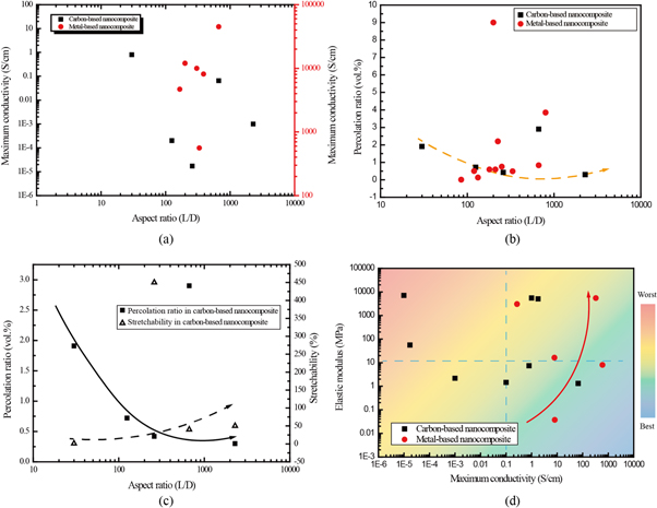
Figure 7. Plot of data points collected from tables 1 and 2. (a) Correlation between the maximum conductivity and aspect ratio of fillers from various nanocomposites. (b) Correlation between the percolation ratio and aspect ratio among various nanocomposites. (c) The trend of the percolation ratio and stretchability with respect to the aspect ratio for carbon-based nanocomposites. (d) The mapping of data points with the elastic modulus against the maximum conductivity.
Download figure:
Standard image High-resolution imageWhere,  is the Planck's constant,
  is the mass of electron and
  is the difference in work function between filler and polymer matrix. However, this tunnelling effect can be ignored if the wrapped polymer between adjacent nanowires is thicker than a cutoff distance
  [92].
[92].
4.2.2. Elastic modulus of composite materials
The studies estimating the elastic modulus of composite materials can date back to the 1970s [93]. The general form for the elastic modulus of a nanocomposite is described as [94]:

Where M represents the elastic modulus of composite and M1 and M2 are the modulus of polymer matrix and filler respectively.  is the volume fraction of fillers and A is a critical parameter defined by the geometry of filler and the Poisson's ratio of polymer matrix. This general equation skips some factors such as the sediments and aggregations of fillers, but it gives a fair estimation of the mechanical property of the resulting composite.
4.2.3. Carbon-based nanocomposite
Carbon particles are often used as conductive fillers because they are widely available, have high electrical conductivity and low cost. Many studies on carbon-based composites in stretchable interconnects are listed in table 1. It can be noted that graphite is one of the most widely used carbon fillers for stretchable and conformable electrodes. In order to achieve the desired level of electrical conductivity a large amount of fillers are used, which also leads to the degradation of stretchability in graphite-based composites [95]. On the other hand, owing the high aspect ratio of CNTs, the conductivity of CNT-based nanocomposites can be higher with a much lower percolation threshold [96]. However, due to the strong Van der Waal forces among carbon fillers, they tend to bundle and entangle together which leads to an inhomogeneous conductivity and high load ratio. By evaluating the maximum conductivity of various nanocomposites, it is observed that the group of Graphene Nanoplatelets nanocomposites exhibit superior conductivity with a low percolation ratio. This is because graphene has large surface area of 2630 m2g−1 and high electrical conductivity 7200 s · m−1 [97].
Table 1. Comparison of various nanocomposites based on carbon fillers with respect to properties such as filler size, percolation ratio, maximum conductivity and mechanical elasticity.
| Material (Filler-polymer matrix) | Filler size | Aspect ratio (L/D) | Percolation ratio | Maximum conductivity | Elastic Modulus | Elongation | Reference |
|---|---|---|---|---|---|---|---|
| Graphite-PDMS | 25.4 μm | — | 11.1 vol.% | 1.8 S cm−1 | 5.1 GPa | 0.71% | [95] |
| Graphite-PDMS | 10 μm | — | 12 vol.% | 2 × 10⁻⁶ S cm−1 | — | — | [98] |
| Graphite-Epoxy | D: 10 μm, | — | 1.3 vol.% | 1 S cm−1 | 5.56 GPa | — | [99] |
| t: 0.1 μm | |||||||
| Graphite-PUa | D: 10 μm, | — | 1.7 vol.% | 1 × 10⁻⁵ S cm−1 | 7.14 GPa | — | [99] |
| t: 0.1 μm | |||||||
| Graphite-Epoxy | 4–44 μm | — | 20 vol.% | 3.3 × 10⁻² S cm−1 | — | — | [100] |
| Graphite-Phenolic Resin | < 1 μm | — | 15 vol.% | 66.7 S cm−1 | 1.3 MPa | — | [101] |
| Graphite-PPb | 21.3 μm | — | — | 20.16 S cm−1 | — | — | [102] |
| Graphite-PVDFc | 21.3 μm | — | — | 0.56 S cm−1 | — | — | [102] |
| Graphite-LDPEd | 2.1–82.6 μm | — | 2.1 μm → 13.5 vol.% | 1 S cm−1 | — | — | [103] |
| 82.6 μm → 25.5 vol.% | |||||||
| eEG-PANI | L: 400 nm, | — | 0.91 vol.% | 35 S cm−1 | — | — | [104] |
| t: 10–40 nm | |||||||
| fGNP- PEg | L: 39–115 nm | — | 0.51, 1.2, 2.4 vol.% | — | — | — | [105] |
| t: 3.6–7.1 nm | |||||||
| hG-ODA-PDMS | t: 2.7 nm | — | 0.63 vol.% | 2 × 10⁻⁶ S cm−1 | — | — | [97] |
| Graphite-PSi | D: 6.5 μm, | — | 3.5 vol.% | 1 × 10⁻⁵ S cm−1 | — | — | [106] |
| t: 100–300 nm | |||||||
| jMWCNT-PDMS | L: 1–25 μm | — | 2.1 vol.% | 0.1 S cm−1 | 1.43 MPa | 45% | [96 |
| MWCNT-PDMS | L: 5–15 μm | ||||||
| D: 60–100 nm | 125 | 0.72 vol.% | 2 × 10⁻⁴ S cm−1 | — | — | [107] | |
| MWCNT-PDMS | L: 30–50 μm | 2285 | 0.3 vol.% | 1 × 10⁻³ S cm−1 | 2.18 MPa | 50% | [108] |
| D: 15–20 nm | |||||||
| MWCNT-PDMS | L: 10–30 μm | 666 | 2.9 vol.% | 6.5 × 10⁻² S cm−1 | — | 40% | [61] |
| D: 20–40 nm | |||||||
| MWCNT-PDMS | L: 1–2 μm | 30 | 1.91 vol.% | 0.8 S cm−1 | 7.38 MPa | 1.2% | [109] |
| D: 40–60 nm | |||||||
| kCNF-PU | L: 30 μm | 260 | 0.42 vol.% | 1.72 × 10⁻⁵ S cm−1 | 56 MPa | 450% | [110] |
| D: 80–150 nm |
aPU: Polyurethanes, bPP: Polypropylene, cPVDF: Poly(vinylidene fluoride), dLDPE: Low density polyethylene, eEG: Exfoliated graphite, fGNP: Graphene Nanoplatelets, gPE: Polyethylene, hG-ODA: Alkyl-functionalized graphene, iPS: Polyester, jMWCNT: Multi-walled carbon nanotube, kCNF: Carbon Nanofiber.
4.2.4. Metal-based nanocomposites
Metal-based composites generally comprise of metallic nanoparticles or nanowire (NWs) as filler materials. They are popular owing to their higher conductivity compared to carbon-based fillers. Silver flakes are often found in commercially available conductive inks. Recently, stretchable and conductive silver-based inks have been commercialized as well [84]. The reported silver ink shows a high conductivity in the range of 103–104 S cm−1, as shown in table 2. The high aspect ratio AgNW further enhances the electrical conductivity. However, the maximum conductivity of the AgNW nanocomposite does not indicate a strong correlation with the aspect ratio of NWs. In general, the percolation ratio of AgNW nanocomposites is low. With a minimum ratio of 0.005 vol.%, their conductivity can reach 2.3 × 10⁻² S cm−1 [111]. On average, the stretchability of AgNW nanocomposites can reach 115%, which makes AgNW nanocomposites good candidates for stretchable interconnects. Some other metallic NW-based composites show a similar performance to AgNWs. Although metal-NWs have the advantages of higher conductivity with a lower elastic modulus suitable for stretchable interconnects, they are not free from challenges. For example, since metallic NWs are manufactured in a solution-based method the insulating ligands in the solvent should be removed to obtain a low contact resistance between adjacent NWs. Usually, a post-treatment process such as thermal annealing is introduced for this purpose and this poses a challenge for devices on polymeric substrates. The idea of introducing a conductive polymer PEDOT:PSS to realize the nano-soldering process among wires dramatically improves the performance of interconnects [112]. Other solutions, such as a hybrid system with AgNWs and other materials (CNTs [113] and Graphene [114]) also show a highly stretchable and conductive performance.
Table 2. Comparison of various nanocomposites based on metal fillers in terms of properties such as filler geometry, percolation ratio, maximum conductivity and mechanical elasticity.
| Material (filler-polymer matrix) | Filler size | Aspect ratio (L/D) | Percolation ratio | Maximum conductivity | Elastic Modulus | Elongation | Reference |
|---|---|---|---|---|---|---|---|
| Ag flakes-PU | 2–3 μm | — | 56 vol.% | 3.6 × 10³ S cm−1 | — | 600% | [115] |
| AgNW-poly(acrylate) | L: 5–15 μm | 83–250 | — | 7.84 S cm−1 | 16.25 MPa | 50% | [116] |
| D: 60 nm | |||||||
| Ag Powder-PDMS | 2–3.5 μm | — | 12.6 vol. % | 6 × 10² S cm−1 | 8 MPa | 150% | [117] |
| AgNW-PUAa | L: 15–25 μm | 666 | 0.83 vol.% | 4.5 × 10⁴ S cm−1 | — | 70% | [71] |
| D: 25–35 nm | |||||||
| AgNW-PDMS | L: 20–50 μm | 304 | — | 9.97 × 10³ S cm−1 | — | 100% | [118] |
| D: 115 nm | |||||||
| AgNW-PDMS | L: 10–60 μm | 388 | — | 8.13 × 10³ S cm−1 | — | 15% | [119] |
| D: 90 nm | |||||||
| Ag flakes-PU | — | — | — | 4.31 × 10⁴ S cm−1 | — | 74% | [84] |
| AgNW-PDMS | L: 10 μm | 166 | — | 4.69 × 10³ S cm−1 | — | 150% | [120] |
| D: 60 nm | |||||||
| AgNW-PDMS | L: 10–60 μm | 388 | — | 8.13 × 10³ S cm−1 | — | 80% | [121] |
| D: 90 nm | |||||||
| AgNW-PDMS | L: 80 μm | 800 | 3.85 vol.% | 20 S cm−1 | — | 35% | [122] |
| D: 100 nm | |||||||
| AgNW-poly(TBA-co-AA)b | L: 20 μm | 333 | — | 5.6 × 10² S cm−1 | — | 160% | [123] |
| D: 60 nm | |||||||
| AgNW-PLAc | L: 8 μm | 133 | 0.13 vol.% | 0.27 S cm−1 | 3048 MPa | 3% | [124] |
| D: 60 nm | |||||||
| AgNW-MCd | — | — | 0.29 vol.% | 3.3 × 10² S cm−1 | 5519.9 MPa | — | [125] |
| AgNW-PEDOT:PSS | L: 10–30 μm | 222 | 2.5% Areal fraction | 104 S cm−1 | — | — | [126] |
| D: 90 nm | |||||||
| AgNW-PEDOT:PSS | L: 50–100 μm | 7500 | — | 0.73 × 10³ S cm−1 | — | 120% | [127] |
| D: 10 nm | |||||||
| AgNW-PEKKe | L: 10–100 μm | 211 | 0.59 vol.% | 1 S cm−1 | — | — | [128] |
| D: 120–400 nm | |||||||
| AgNW-PCf | L: 10 μm | 85 | 0.005 vol.% | 2.3 × 10⁻² S cm−1 | — | — | [111] |
| D: 117 nm | |||||||
| AgNW-PA11g | L: 30–60 μm | 180 | 0.59 vol.% | 2.7 S cm−1 | — | — | [129] |
| D: 200–300 nm | |||||||
| AgNW-PS | L: 10–60 μm | 333 | 0.489 vol.% | 10 S cm−1 | — | — | [130] |
| D: 70–140 nm | |||||||
| AgNW-SBSh | L: 30 μm | 200 | 9 vol.% | 1.2 × 10⁴ S cm−1 | — | 100% | [83] |
| D: 150 nm | |||||||
| CuNW-PVAi-PDMS | L: 20 μm | 333 | — | 8.1 S cm−1 | 37.5 kPa | 60% | [131] |
| D: 60 nm | |||||||
| CuNW-GFRHybrimerj | L: 35 μm | 700 | — | 4.8 S cm−1 | — | — | [132] |
| D: 50 nm | |||||||
| CuNW-PS | L: 3 μm | 120 | 0.25–0.75 vol.% | 10−6 S cm−1 | — | — | [133] |
| D: 25 nm | |||||||
| CuZr-PDMS | — | — | — | 1.32 × 10⁴ S cm−1 | — | 70% | [134] |
| NiNW-P(VDF-TrFE)k | L: 50 μm | 250 | 0.75 vol.% | 1 S cm−1 | — | — | [135] |
| D: 200 nm | |||||||
| AuNW-P(VDF-TrFE) | L: 45 μm | 225 | 2.2 vol.% | 1 S cm−1 | — | — | [136] |
| D: 200 nm |
aPUA: Polyurethane acrylate, bPoly(TBA-co-AA): Poly(tert-butylacrylate-co-acrylic acid), cPLA: Polylactide, dMC: Methylcellulose, ePEKK: Poly(ether ketone ketone), fPC: Polycarbonate, gPA11: Polyamide 11, hSBS: Styrene butadiene styrene, iPVA: Poly(vinyl alcohol), jGFRHybrimer: Glass-fabric reinforced plastic film, kP(VDF-TrFE): Poly(vinylidene difluoride)- trifluoroethylene.
4.3. Discussion
4.3.1.
Studying the data from tables 1 and 2, the correlation among many factors such as material type, aspect ratio of fillers, percolation ratio, and elastic modulus in the nanocomposite can be established. As shown in figure 7(a), even with a similar aspect ratio of the filler, the maximum achieved conductivity of a metal-based nanocomposite is several orders higher than a carbon-based nanocomposite. This is due to the high electrical conductivity of metal. From the plots, it is clear that the maximum conductivity does not show any reliance on the filler's aspect ratio. However, the aspect ratio has a strong effect on the percolation ratio as shown in figure 7. Viewed from the data illustrated in figure 7(b), the four data points from the carbon-based nanocomposite are all composed of MWCNTs with PDMS and this excludes the influence of material property. The trend, indicated in dashed line, shows a reciprocal relation between the aspect ratio of the filler and the percolation ratio, which matches with theoretical relationship in equation (2). In contrast, the metal-nanocomposites do not reveal any such trend. Within a large range of aspect ratio of metal fillers (100–1000), nanocomposites have a low percolation ratio (<1 vol.%). This could be attributed to the fact that the metal fillers, as compared to the carbon fillers, do not get entangled due to their straightness and passive oxide structure. The SEM images in figure 8 compare the CNT with metal NWs. It can be seen the CNT has a tortuous morphology while the AgNWs are straight. The influence of the filler's aspect ratio is not only reflected in a reduced percolation ratio, but also in the improved stretchability. If the parameter of stretchability is added into the diagram between the aspect ratio and percolation ratio of the carbon-based nanocomposite (figure 7(c)), it is clear that the high aspect ratio of the fillers gives higher stretchability. In practice, there is always a trade-off. The higher the ratio of fillers, the higher the conductivity of the nanocomposite, and the lower the elastic property. According to the collection of data points presented in figure 7(d), most points of carbon-based nanocomposites lie below the conductivity of 1 S cm−1 with a large difference in the elastic modulus. In contrast, a trend indicated by the red arrow line can be found in metal-based nanocomposites, of which the higher conductivity leads to a higher elastic modulus. Still, a point with high conductivity (∼10 S cm−1) and low elastic modulus (∼40 kPa) can be found. The blue highlighted area indicates the region suitable for stretchable interconnects while the red area is the direction that should to be avoided.
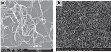
Figure 8. SEM images of (a) a carbon nanotube. Reprinted from [144], copyright 2013, with permission from Elsevier. (b) AgNWs. Reproduced from [145]. © IOP Publishing Ltd. All rights reserved.
Download figure:
Standard image High-resolution image5. Application
A wide range of applications requiring stretchable interconnects are shown in figure 9. In these applications, only flexibility of the electronic system is insufficient to meet the requirements as they experience large deformations during bending. The development of stretchable interconnects to integrate multifunctional sensors and electronics has filled this gap and in fact the field has grown exponentially in line with the trend presented in figure 1. Figure 9(a) shows the serpentine-shaped stretchable interconnects realized with a MWCNT-PDMS nanocomposite. Figure 9(b) demonstrates a smart prosthetic hand equipped with artificial skin that is able to detect various signals such as humidity, temperature, pressure, etc [137]. Some applications of stretchable electronics can make a huge difference and accelerate the progress of medical treatment. For example, the balloon catheter often used in surgery to eliminate blood blockage requires up to 130% stretching when inflated. Stretchable interconnects on such a balloon catheter with pressure sensors is illustrated in figure 9(c). The stretchable interconnects enable the overall electronic system to withstand large deformation while giving electrical feedback to surgeons in order to help improve the performance of surgery [1]. Other clinically relevant information like temperature can be monitored from human skin in situ (figure 9(d)) [138]. In this case, a 24 h or even longer time thermometry data can be collected by the surgeon or clinician, which can improve medical treatments. For applications where more precise surgeries and signal monitoring are required, stretchable neural electrodes [33] have been developed. Applications in wearable electronics for motion detection (figure 9(e)) have also benefited from stretchable electronics. These applications have integrated electronics to wearable cloths such as bandages and gloves [139]. Not only have stretchable mechanical sensors have been developed, stretchable chemical sensors have also shown promising results. The complete stretchable device shown in figure 9(f) is able to give an epidermal analysis of biofluids like sweat and is able to undergo stretching [140, 141]. Regarding consumer electronic applications, stretchable displays have been developed by interconnecting rigid inorganic light emitting diodes (ILED) with non-coplanar stretchable interconnects [142]. For a multifunctional wearable system, the serpentine-shaped stretchable interconnects allow rigid electronic components including signal detection electrodes, inductive power, amplifier and data transmission coil to form a stretchable network as shown in figure 9(h). Such networks enable an efficient method of data collection. Even weak electrophysiological signals can be detected and transmitted. Furthermore, this network is robust against any stretching and twisting movement [143]. Interconnects to form a stretchable circuit can be realized by intrinsic conductive and stretchable materials as shown in figure 9(i). The circuit signals are transmitted through SWNT-based bit/word bus lines. The resulting circuit can be mounted on an arbitrary curved surface and can be further applied on the arm or the joint of a robot [55].

Figure 9. (a) Stretchable interconnects based on a MWCNT-PDMS nanocomposite. (b) Artificial skin for a prosthetic hand. Reprinted by permission from Macmillan Publishers Ltd: Nature Communications [137], copyright 2014. (c) Balloon catheter integrated with electrodes and temperature sensors. Reprinted by permission from Macmillan Publishers Ltd: Nature Materials [1], copyright 2011. (d) Thermal monitoring sensor system for human skin. Reprinted by permission from Macmillan Publishers Ltd: Nature Materials [138], copyright 2013. (e) Strain sensor integrated with a bandage and glove. Reprinted by permission from Macmillan Publishers Ltd: Nature Nanotechnology [139], copyright 2011. (f) Stretchable chemical sensor for sweat detection [141] John Wiley & Sons. © 2014 WILEY-VCH Verlag GmbH & Co. KGaA, Weinheim. (g) Stretchable display based on an inorganic LED. From [142]. Reprinted with permission from AAAS. (h) Stretchable circuits for EEG signal detection and transmission. From [143]. Reprinted with permission from AAAS; and (i) a stretchable transistor matrix. From [55]. Reprinted with permission from AAAS.
Download figure:
Standard image High-resolution image
6. Conclusion
This article presents an overview of the various technologies and materials that have been used for stretchable interconnects. In particular, our focus has been on printable nanocomposites as they enable systems with intrinsic stretchability and excellent electrical conductivity. With innovative designs these interconnect structures could allow electronic systems to withstand strain up to 200%. By incorporating intrinsic and stretchable materials, the tolerable strain can be even larger. Among the various materials, rubber-like nanocomposites draw major attention because of their high electrical performance and softness. The filler-polymer matrix system is summarized according to the filler materials, which includes carbon-based and metal-based fillers. Due to the difference in the morphology, size, and electrical conductivity of dispersed fillers, the trends in percolation ratio, maximum electrical conductivity and elastic modulus of resultant nanocomposites between carbon-based and metal-based nanocomposites exhibit different behaviors. In general, high aspect ratio NWs are preferred as fillers for nanocomposites as they allow one to maintain a low electrical percolation threshold and high stretchability. Compared with metal-based fillers, carbon-based fillers have advantages in terms of low cost and less degradation (oxidation, etc) during processing. If metal-based fillers are dealt with carefully, they can be more suitable for stretchable interconnect applications. The in-depth analysis of printed nanocomposite-based stretchable interconnects presented in this paper will offer an excellent guide for researchers in this field and flexible electronics in general.
Acknowledgments
This work was supported by the European Commission under grant agreement PITN-GA-2012-317488-CONTEST and Engineering and Physical Sciences Council (EPSRC) Fellowship for Growth—Printable Tactile Skin (EP/M002527/1).