

Abstract
Emerging from 2D printed electronics, 3D printed electronics promise a break-through in additive manufacturing and prototyping of electronics. However, transferring the know-how from 2D flexible electronics to 3D parts with complex structures (e.g. internal vias and external interconnects) might not be a straightforward approach. As an example, the variation of light intensity with respect to the distance and angle of incidence casts doubt on the efficiency of the intense pulsed laser (IPL) as a robust sintering method for metallic traces in 3D printed bulk structures, whereas IPL is currently by far the most prevailing sintering technique for 2D printed flexible electronics. Sintering of metallic traces in 3D printed parts can be executed either as a sequential layer-by-layer printing and processing step (LP) or as a bulk post-processing step (BP). In the current study, a survey on the most common sintering strategies for inkjet printed silver nanoparticles was conducted, while the compatibility to 3D printed structures was brought into the focal point. To discover the capabilities and limitations of six sintering methods (i. e. IPL, ohmic curing, thermal heating, laser, atmospheric plasma and microwave sintering) for 3D printed electronics, a comparative study utilizing the same materials and diagnostic methods was pursued. The results revealed that for 3D functional parts, some of the sintering techniques can be considered as complementary methods for each other, whereas a few showed readily the potential to be adapted in 3D printed electronics production.
Export citation and abstract BibTeX RIS

Original content from this work may be used under the terms of the Creative Commons Attribution 3.0 licence. Any further distribution of this work must maintain attribution to the author(s) and the title of the work, journal citation and DOI.
Introduction
Light weight, inexpensive and flexible electronic devices have seen a strong growth over the last decade. The development of versatile fabrication techniques for high throughput roll to roll (R2R) production lines enabled the printed electronics to move even further toward a cost-effective, mature technology. On the other hand, despite the growing interest toward 3D additive manufacturing, the current fabrication of most printed electronics is still limited to the conventional 2D tags and sensors [1]. Microfabrication of 3D hybrid structures composed of several functional materials in a layer-by-layer processing can be seen as a novel prospect for additive manufacturing industries. For instance, the new concept of rapid advanced packaging of prototypes by exploiting the flexibility of photopolymers and versatility of inkjet printing of conductive contacts was introduced recently [2, 3]. Inkjet printing of metal containing inks has been widely accepted as a versatile tool for the fabrication of contacts and interconnects in an additive, digital and non-contact manner at relatively high speed that enables R2R production. Inkjet printing inks consist of metallic nanoparticles (NP) suspensions with colloidal stabilizers to prevent particle flocculation or nozzle clogging and are frequently used for conductive tracks. Silver, copper and gold NPs are the most common metals in that regard [3–6].
Most of the commercially available and widely-used inkjet printing platforms are limited to only printing the inks and are normally not equipped with a method to sinter the NPs into conductive traces after the deposition. The as-printed patterns using NP inks usually have a large resistivity and require a following sintering process at mild temperatures (30–60 min at 100 °C–200 °C for silver NP) [7]. As a result of this thermal treatment, the conductivity of the patterns will be subsequently enhanced by promoting the necking among the NPs and removal of electrically non-conductive organic components.
Because of the thermoplastic nature of plastic flexible substrates, the relatively high sintering temperature of NP inks restricts the choice of certain substrates. Consequently, alternative sintering approaches, such as intense pulsed light sintering (IPL), electrical sintering (also known as ohmic heating), laser, atmospheric plasma and microwave sintering were proposed and their compatibility to 2D flexible electronics were studied [8]. All these techniques are capable of sintering at a relatively low processing temperature. To this time, some techniques such as microwave, plasma and electrical sintering have been performed only on a small laboratory scale, while some others such as IPL and laser sintering have gained the maturity and reliability to be implemented in a compatible R2R production line. Beside the above-mentioned techniques, chemical sintering was also reported on laboratory scale to be practicable primarily for metal organic compounds [9].
Amongst these sintering techniques, IPL attracted a lot of attention as the most promising alternative sintering technique to replace conventional thermal sintering, in terms of short processing times for low temperature 2D substrates and promising scale-up potential for R2R fabrication [8, 9]. In IPL sintering, a xenon lamp emits radiation with the wavelengths between UV and IR with highest intensity in the visible range. An intense pulse of radiation with duration shorter than the thermal equilibration time of NPs and substrate, heat the NPs quickly enough to sinter before they transfer much energy to the substrate [10]. However IPL seems to have evident shortfalls with respect to 3D structures. As implied from inverse square law formula of the light radiation, when the distance from a light source (d) increases, the intensity of light decreases by the factor of 1/d2 [11]. Therefore, considering two contacts in different heights of a 3D structure, when the optimal sintering condition for one of them is being applied, the other one will be either ablated (over-sintered) or not thoroughly sintered. In addition, according to the Lambert's cosine law, the illumination at a point in an oblique surface is proportional to the cosine of the angle which the incident luminous flux makes with the normal of the surface [12]. In another words, in the complex 3D structure, if the printed lines lie on the surface inclined to the light falling on it, illumination is weaker, which in turn leads to inhomogeneous or deficient sintering. These two weaknesses emerging from the characteristics of 3D structures yield to the conclusion that IPL solely might not be presumed to be the first answer for every sintering scenario.
Consequently, a reassessment of the sintering techniques with respect to 3D printed electronics seems to be necessary. To discover the capabilities and limitations of the above-mentioned sintering methods, in this study, a comparative study utilizing the same materials and diagnostic methods was pursued. A feasibility analysis based on the conductivity measurements was performed and various critical parameters such as selectivity of the sintering techniques, upscalability for R2R fabrication, and compatibility to 3D structures were discussed.
Experimental procedure
An advanced R&D inkjet printer (PiXDRO LP50, Meyer Burger Technology AG) equipped with an industrial inkjet print-head (SM-128 SpectraS-class, Fujifilm Dimatix Inc.,) with a 50 μm nozzle diameter and 50 pl calibrated drop size was utilized. The nanoparticle Ag ink (Sycris I50DB-114, PV Nanocell) with 50 wt% metal loading and average particle size of 110 nm (d90) was deposited at the operational jetting voltage of 100 V, printing frequency of 500 Hz and at carefully adjusted jetting pulse duration profile. The print-head was jetting at room temperature, while the substrate was heated-up to 50 °C.
Two types of substrates were selected for this study; 2D foil and 3D printed polymeric substrates. In the case of 2D substrate, overhead transparent foils (cellulose acetate) with a thickness of 100 μm were used as substrate with a glass transition temperature (Tg) of maximum 130 °C. The pattern of the printed sample is depicted in figure 1. The pattern consists of a 20 mm × 0.3 mm line with two triangle pads at the ends. A typical configuration of a printed line after drying obtained by a mechanical stylus profilometer (Dektak XT-A, Brucker) is also shown in figure 1. Several identical printed tracks were inkjetted on a A4 sheet substrate. The sheet resistance of the printed structures was measured using a four-point probe technique (C4S, Cascade Microtech GmbH). In the case of 3D structures, 3D printed test blocks made of a translucent acrylate-type polymer (Tg = 65 °C, VisiJet M3 Crystal) were printed by using a high-performance multi-jet 3D printer (ProJet 3510 HDPlus, 3D Systems). In figure 2, two 3D printed test blocks are shown, featuring series of inclined and stepped patterns in various angles and sizes to mimic the geometry of complex 3D printed devices.
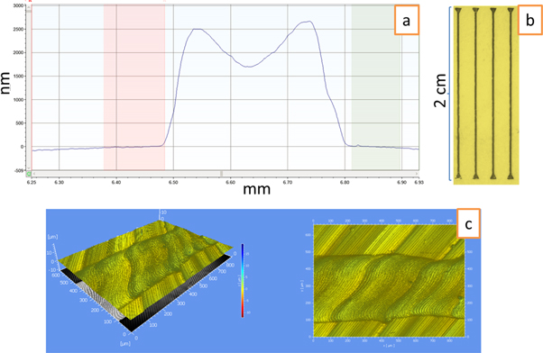
Figure 1. Surface profile of the printed Ag tracks (a), the dimension (b) and the corresponding 3D surface topography.
Download figure:
Standard image High-resolution image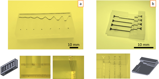
Figure 2. 3D printed test blocks in two configurations to realize the inclined (a) and stepped (b) metallic structures in 3D printed electronics.
Download figure:
Standard image High-resolution imageA white-light interferometer (WLI, MSA-500-TPM, Polytec) was used for topography characterization of the substrate and printed lines. The morphology of the printed track before and after curing was characterized using scanning electron microscopy (SEM, Quanta 200 FEGSEM, FEI) and focused ion beam workstation (FIB, Quanta 200 3D, FEI). A Pt-based thin layer was deposited onto the surface in order to protect the surface of printed traces from incurring FIB induced damage.
Sintering techniques
The IPL sintering was performed by means of a photonic sintering device (PulseForge 1200, Novacentrix). The IPL device offers several processing parameters such as lamp voltage, pulse shape, pulse numbers and pulse duration which influence the sintering performance. However, in this study, the corresponding energy density of light exposure which is determined by lamp voltage, pulse shape and duration is reported. Thermal sintering was carried out in a conventional oven. Although the recommended thermal sintering of the ink on glass substrate was aimed for higher temperatures, with respect to the glass transition temperature of polymeric 3D substrates and 2D foils, 65 °C and 130 °C were determined as the maximum sintering temperatures (Tmax) respectively. Accordingly, the samples were subjected to a sintering cycle by gradually increasing the temperature from the ambient temperature to Tmax in 30 min, followed by a dwell time of 3 h at Tmax and cooling down in 30 min.
Some samples were cured in a commercial microwave oven (LG MS2389B, providing 800 W at 2.45 GHz) for comparison. Atmospheric pressure plasma sintering was also exercised using a manual plasma piezobrush® (PZ2, Reylon plasma GmbH) in which a direct, electric discharge at an openly operated piezoelectric transformer (OPT) is implemented to dissociate and ionize the ambient process gas (air). In OPT, the transformer provides the discharge, whereas neither a secondary electrode, nor an electric filed other than the discharge are required. At a maximum power consumption of 30 W, cold active plasma with a temperature of ∼50 °C was generated. Laser sintering was performed utilizing a near-infrared (NIR) diode laser operating in a continuous wave mode with a wavelength of λ = 808 nm and nominal power output of 400 mW. The laser was mounted on an automated stage equipped with a high magnification optical microscope; thereby the precise positioning of the printed tracks with respect to laser spot was enabled. The optimal sweeping speed of the laser was determined to be 1.1 mm s−1. Ohmic sintering was conducted by implementing a programmable linear regulated DC power supply (PL 303-P, Aim-TTI instruments) connected to a personal computer and controlled by a LAB-VIEW software developed by CTR.
Results and discussion
Chronologically, sintering of metallic traces in 3D printed parts can be implemented either as a sequential layer-by-layer printing and processing step (LP) or as a bulk post-processing step (BP). LP can be simply differentiated from BP, since LP is essentially an accumulative 2D sintering process. Therefore, the results obtained from the 2D substrates principally can be applied to 3D structures built-up by LP processing. Thus, in this study, sintering strategies of two types of substrate (i.e. 2D foils and 3D printed bulks) which respectively resembled LP and BP processing were investigated. The 2D and 3D printed substrates are shown in figures 1 and 2, respectively.
As explained by de Gnas and Schubert [13], upon drying of a deposited ink, a capillary-driven flow from the droplet center toward the edge compensates for evaporation losses and transports most of the solute toward the edge; therefore a mild concave profile was typically resulted after inkjet printing and drying at 50 °C. This mechanism is also known as the coffee ring effect or in some instances, the coffee stain effect. The associated topography of the tracks prior to sintering is depicted in figure 1. Correspondingly, the top view and cross-sectional images of the tracks after sintering via laser, IPL, thermal and ohmic techniques are shown in figure 3.

Figure 3. Top view and cross-sectional images of the sintered Ag tracks via laser, IPL, thermal and ohmic techniques.
Download figure:
Standard image High-resolution imageOhmic sintering is principally an exploitation of electrical current across a conductive trace to produce ohmic heating to cure selectively printed traces. An essential processing step prior to ohmic curing is a pre-treatment step to achieve a relatively conductive state [14, 15]. The results reveal that for our ink/substrate combination an initial conductivity of at least 0.15% of bulk silver was required, which was facilitated by either IPL pre-sintering or thermal pre-heating. It is noteworthy to mention that, provided the initial conductivity higher than 0.1 MΩ−1 m−1 (>0.15% of bulk Ag), the final conductivity of the traces would be only a function of applied electrical current and independent from the initial value. As a matter of fact, when the initial conductivity was lower than 0.1 MΩ−1 m−1, no detectable changes in resistance upon ohmic sintering was observed. As plotted in figure 4(a), by applying the electrical current, the resistance decreases abruptly to the constant value, which varies afterwards only marginally with time. Apparently, the sintering process took place within a few seconds. By comparison, one can perceive a direct correlation between the input current and the final resistance, which is plotted in figure 4(b).
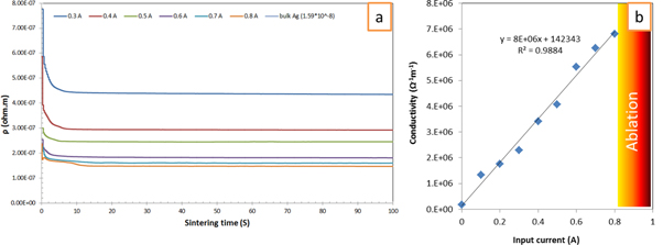
Figure 4. The enhancement of conductivity by increasing sintering time (a) and input current (b) in the course of ohmic curing.
Download figure:
Standard image High-resolution imageAs inferred from figure 5, the surface morphology of the tracks was significantly changed after ohmic curing, which is a characteristic fingerprint of ohmic sintering. In fact, since in ohmic sintering the printed track has to be contacted from one end to the other end, one narrow percolation path is generated within the track. After reaching certain conductivity, the ohmic heating effects are not sufficient enough to sinter the surroundings of the initial percolation path [9]. This phenomenon disclosed a remarkable drawback for DC ohmic curing, which produces two distinctive regions after curing; sintered and not affected. On the other hand, since electrical sintering can be carried out in a very selective manner, by rinsing the un-sintered regions in which inferior adhesion to substrate exists, the width of the tracks reduces; i.e., the resolution of the printed tracks increases. Moreover, direct contacting of the printed tracks upon ohmic curing provides an in situ monitoring of the progress of sintering, which allows tailoring the obtained conductivity by defining the maximum current.

Figure 5. Morphological evolution of Ag track upon ohmic sintering; before (a), after sintering with 0.6 A (b), and over-sintering with 1.5 A (c). The formation of narrow percolation paths are shown in (b)–(e).
Download figure:
Standard image High-resolution imageThe WLI micrographs of laser sintering at different optical powers (mW) are presented in figure 6. As implied from these figures, with increasing the optical power, the area affected by laser treatment is respectively expanding. As a consequence, the conductivity of the tracks remarkably enhanced with increasing the laser power (figure 7(a)). The laser spot was originally calculated and designated to be around 200 μm, in order to avoid exposure to the substrate. However, as implied from figure 6, lower optical power leads to even smaller laser affected zones. As seen in figure 6, when the optical power of the laser was set to be 63 mW, the laser affected zone had a width of 95.2 μm; whereas by 251 mW optical power, the width increased to 235.4 μm.

Figure 6. The effect of laser optical power on the extent and shape of sintered area.
Download figure:
Standard image High-resolution image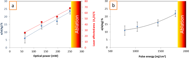
Figure 7. Relative conductivity as a function of laser optical power (a) and IPL pulse energy (b).
Download figure:
Standard image High-resolution imageAnother distinctive evolution upon laser sintering similar to ohmic sintering is the intensified concaved (coffee-staining like) shape of the tracks, manifesting a high localized temperature zone. As a matter of fact three sequential steps occur in the sintering process of metal NP inks: (1) evaporation of the solvent; (2) removal of dispersants and binder materials by thermal decomposition; and (3) neck formation and grain growth [16]. The first two steps coincide with severe volume shrinkage up to ∼50 wt% in our case. In fact, one of the main drawbacks of the rapid sintering processes in comparison to thermal sintering is the appearance of a rough or uneven surface due to instantaneous volume reduction of the material and the fast volatilization of organic matter. Consequently, a fast and selective sintering process such as laser sintering clearly differentiates the sintered and un-sintered regions from their configurations. On the other hand, laser processing can produce high resolution and lithography free printed lines by selective sintering at the central part of the inkjet printed NPs and by washing out the un-sintered structures [16]. Laser sintering locally heats up the area for a very short period of time, but the temperature may rise temporarily above the Tg of the substrate [8]. Hence, it was speculated that employing higher optical power could adversely affect and decompose the polymeric substrate. NIR lasers have a low absorption and large transmittance through the metallic NPs and therefore diffuse inside the substrate/ink interface, leading to a bottom to top sintering progress [17]. According to Maekawa et al [17], this phenomenon yield to better adhesion and denser structure. On the other hand, visible lasers with high absorption and low transmittance on the ink develop rapid metallization and activate solvent evaporation, resulting in a rough surface with large pores. Moreover, the probability of surface ablation due to excessive surface heating is higher for lasers operating at visible wavelength, whereas the chance to damage the substrate is higher for lasers operating at NIR wavelength.
As noted before, IPL sintering of 3D parts encounters serious shortfalls, which restricts its efficiency to 2.5 D parts. Optical images in figure 8 clearly manifest the deficiency of sintering of 3D bulk structures by means of IPL. As seen, the features on the upper surface are exposed to higher intensity of light, thereby ablated, whereas the features on the lower surface are either sintered or partially sintered. In fact, the aforementioned limitations for IPL are decisive when sintering is implemented as a BP processing. However, if integrated in a LP processing, IPL can represent itself again as a robust approach. As shown in figure 7(b), by increasing the energy density, the conductivity of 2D structures was significantly enhanced.
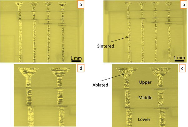
Figure 8. Micrographs of the metallic tracks before (a), (d) and after IPL sintering (b), (c), indicating an inhomogeneous sintering of 3D patterns.
Download figure:
Standard image High-resolution imageDespite the fact that the thermal sintering is typically a long process with restrictions for temperature-sensitive materials, the comparison between the conductivity obtained by this method and others is worthwhile. In figure 3 the corresponding micrographs of thermal sintering are compared with those of IPL, laser and ohmic sintering. As inferred from the top view and cross-sectional images in this figure, sintering via thermal sintering renders a uniform structure, due to the sufficient atomic diffusion. Since grain-boundary diffusion and volume diffusion rely heavily upon temperature and time, thermal sintering yield to a homogeneous microstructure. It was also speculated that the grain growth mechanisms could be attributed to the relatively denser microstructure of thermal sintering (figure 3(g)).
Microwave sintering was also proposed and examined as a viable contactless strategy for curing 3D traces. The penetration depth for microwave with the frequency of 2.45 GHz into metals is approximately 2 μm, which matches well to the thickness of inkjet printed Ag tracks. Moreover, the polymeric substrates are also transparent to microwaves [18]. Nonetheless, several issues such as desired pre-sintering steps and conductive antennas, emergence of frequent hotspots and sensitivity to the shape of the printed pattern cast doubt on its feasibility for R2R production lines. An initial conductivity of 0.1% of bulk Ag was reported to be required for successful microwave sintering [19], which for our ink/substrate combination was ∼0.5% of bulk Ag. As shown in figure 9, the appearance of random hotspots during sintering result in inhomogeneous heating, thereby deficient sintering, which hinders the controllability of the sintering process. The highest reliable conductance (with less than 10% of the failure) was around ∼11% of bulk Ag.

Figure 9. Formation of hotspots upon microwave sintering.
Download figure:
Standard image High-resolution imageAtmospheric plasma sintering by using a plasma torch was also practiced, leading to a maximum conductivity up to ∼4%–5% of bulk Ag after 30 min. In comparison to low pressure plasma, atmospheric plasma sintering has the advantage of not demanding vacuum processing; thereby it can be compatible with R2R production. However, the electrode distance for atmospheric plasma is restricted down to few millimeters, since the break-down voltage of the plasma is in correlation to both pressure and electrode distance. Allegedly, atmospheric plasma sintering does also suffer from distance variations in 3D bulk structures; applying plasma in different heights of a 3D structure can be challenging. Wünscher et al [20] investigated the influence of the distance between printed features and plasma pencil, by altering the distance from 2 to 6 mm. The results showed a dramatic increase in resistance (4 to 5 orders of magnitudes) when the distance increased from 2 to 6 mm. They attributed this phenomenon to the escalated oxidation of Ag NPs, since the plasma beam in higher distance takes up more oxygen atoms [20]. In addition more, compared to other sintering techniques, plasma sintering is a relatively slow process. Nonetheless, plasma sintering can be regarded rather as a pre-sintering method.
It is noteworthy to indicate that in the literature higher conductivities were reported for each of the practiced techniques, by optimizing the processing parameters, tailoring the ink/substrate properties and employing advanced equipment. The readers are therefore encouraged to peruse the dedicated literature on the corresponding techniques. However, in the current study, the viability of the sintering approaches with respect to 2D and 3D printed electronics was determined as the main goal.
As illustrated in figure 10 the maximum conductivity obtained by IPL and laser were similar to each other (∼23% of bulk Ag) and higher than ohmic (18% of bulk Ag), microwave (11% of bulk Ag) and thermal sintering (8% of bulk Ag). In terms of processing time, however, IPL sintering took only few milliseconds, whereas ohmic and microwave and laser sintering took 5, 10 and 18 s, respectively. Plasma sintering was applied for 30 min. As expected, thermal sintering with the dwell time of 3 h was the longest process.

Figure 10. A comparison among six sintering techniques in terms of the average conductivity of Ag tracks.
Download figure:
Standard image High-resolution image
The results revealed that for 3D functional parts, some of these sintering techniques should be considered as complementary methods to each other, e.g. as a pre-sintering step for ohmic and microwave sintering. Moreover, implementing multiple sintering steps as suggested before [15, 21] revealed promising improvement for rapid sintering techniques, in which a gradual evaporation of the solvent and successively sintering of the NPs is promoted. The results of the current study also indicate that by applying multiple sintering steps with gradual increase in the intensity of input energy, higher conductivity and less failure were enabled.
Considering the lower Tg of the 3D printed material (65 °C), pre-sintering of 3D parts in oven was not as efficient as for the 2D foils with higher Tg (130 °C), rendering a lingered process with inadequate conductivity for ohmic and microwave sintering. The most determining limitation for ohmic and microwave sintering lies in the pre-requisite conductivity of the tracks, when it comes to low-Tg substrates. On the other hand, laser sintering equipped with a programmable 3D moving stage was revealed to be a robust strategy for both LP and BP sintering of 3D structures. Practically speaking, a built-in laser sintering head incorporated in inkjet printer apparatus promises a top-notch, R2R solution for both LP and BP sintering of 3D structures.
Conclusion
This feasibility study was focused on the sintering strategies of inkjet printed Ag tracks on temperature-sensitive substrate with the aim to propose the best candidates for 3D functionalized devices. Table 1 outlines the capabilities and restrictions of sintering techniques. This table clearly has some limitations; nevertheless, it can be a framework for evaluation of sintering techniques with respect to 3D printed electronics. The findings of this investigation can be summarized as follows:
- (1)With respect to LP processing of 3D printed electronics, except ohmic sintering, all other techniques were capable of sintering the printed tracks in a contactless manner.
- (2)The maximum conductivity obtained by IPL and laser were similar to each other (∼23% of bulk Ag) and higher than ohmic (18% of bulk Ag), microwave (11% of bulk Ag), atomospheric plasma (5% of bulk Ag), and thermal sintering (8% of bulk Ag).
- (3)IPL sintering took only few milliseconds, whereas ohmic and microwave and laser sintering took 5, 10 and 18 s, respectively. Plasma sintering was applied for 30 min. As expected, thermal sintering with the dwell time of 3 h was the longest process.
- (4)With respect to BP processing of 3D printed electronics, laser sintering equipped with a programmable 3D moving stage was revealed to be the most robust sintering strategy.
Table 1. Qualitative comparison among sintering techniques.
| Sintering techniques | ||||||
|---|---|---|---|---|---|---|
| Assets | Plasma (Atm) | IPL | Laser | Ohmic | Microwave | Thermal |
| 2D structures | ✓ | ✓✓ | ✓ | ✓ | ✓ | ✓ |
| 3D structures (LPa) | ✓ | ✓ | ✓ | ✓ | ✓ | ✓ |
| 3D structures (BPb) | × | × | ✓ | ✓ | ✓ | ✓ |
| Contactless | ✓ | ✓ | ✓ | × | ✓ | ✓ |
| Homogeneity | ✓ | ✓ | ✓ | × | × | ✓✓ |
| Selectivity | × | × | ✓ | ✓ | × | × |
| Nonconductors | ✓ | ✓ | ✓ | × | × | ✓ |
| Low T substrates | ✓ | ✓ | ∼ | ✓ | ✓ | × |
| Speed | × | ✓ | × | × | ✓ | ×× |
| R2R production | × | ✓ | ✓ | × | ✓ | × |
| Cost | ✓ | × | ✓ | ✓✓ | ✓ | ✓ |
aSequential layer by layer processing step (LP). bBulk post-processing step (BP).
Acknowledgments
This project has received funding from the Electronic Component Systems for European Leadership Joint Undertaking under grant agreement No 692480. This Joint Undertaking receives support from the European Union's Horizon 2020 research and innovation programme and Germany, Saxony, Spain, Austria, Belgium, Slovakia. The project 'IoSense' is co-funded by Austrian Research Promotion Agency (FFG). The authors also want to acknowledge Dr B Abasahl for valuable suggestions and discussions. SEM investigations were carried out using the facilities at the University Service Center for Transmission Electron Microscopy (USTEM) at the Vienna University of Technology.