


Abstract
Functional electronic systems have been screen- or inkjet-printed on different plastic substrates, including polyethylene terephthalate, polycarbonate and polycarbonate/acrylonitrile butadiene styrene blends. Mutual capacitive sensors were designed and printed on flexible substrates and the capacitive response and functionality of the printed sensor with integrated passive electronic components was demonstrated. The applicability of both, inkjet printing and screen printing for the development of such capacitive sensors was evaluated. The influence of the substrate, sensor design and the printing technique parameters on both printability and functionality are discussed. Further, a flexible illumination system was developed, where the printed circuit was combined with surface mounted light emitting diodes and integrated circuits. Finally, the developed capacitive sensors and the illumination system were connected to each other to demonstrate the connectivity and interoperability of the different printed circuit components.
Export citation and abstract BibTeX RIS
1. Introduction
Today's electronics market requires increasingly novel design of electronic components compatible with lower weight, large area and thin film applications, together with low fabrication cost. Therefore, new ways of fabricating electronic devices with flexible materials are being developed. Such requirements can be fulfilled by using printed electronics, which can be applied on a wide range of flexible materials, which are compatible with low cost production techniques. By means of printing, the electronics can be fabricated at low temperature on flexible polymeric substrates, using additive processes. Apart from being flexible, recently, the printed electronics further allows in some cases the electronic devices to become stretchable [1] or mouldable [2]. Stretchable electronics refers to devices, which can deform reversibly maintaining functionality. In-mould electronics (injection-moulding electronics), on the other hand, enables the change of the initial 2D form of the printed device to a 3D form by applying additional post-treatment processes, such as thermoforming or injection moulding. Those technologies open a new possible applications, where electronics needs to be integrated in plastics, in a variety of 3D-shaped forms. At the same time, these processes are compatible with other additive manufacturing technologies and allow to save time and cost in production lines. The manufacturing process of plastic pieces with embedded electronics can be divided into three main steps:
- (a)printing of the electronic circuit on flexible substrates,
- (b)assembly of rigid electronic components, and
- (c)plastic injection and over moulding of the electronic circuit.
In the first step, part of the electronic circuit is printed by means of different possible printing techniques such as inkjet printing [3–5], screen printing [6, 7], gravure/slot-die printing [8], nanoimprinting [9] or 3D-printing [10–12]. For the printing of the electronic circuits, conductive inks based on electrically conductive particles are used. The traces or interconnections between electronic components and some type of sensors consisting of conductive electrodes can be printed directly using conductive inks.
In this context, screen-printing technique highlights due to its printing speed, repeatability and precision. Further, it is characterized by printing simplicity and affordability. On the other hand, inkjet printing uses low viscous inks and it is a contact-less printing method, which makes it more suitable for working with fragile materials. Moreover, inkjet printing minimizes material wastage, thus reducing contamination [13].
Progresses in printing technologies and materials will allow increasing types of sensors and electronic components to be printed using not only conductive inks, but also different functional materials such as dielectric, piezoelectric or piezoresistive inks [14, 15]. However, to improve performance of the circuits, it is still necessary to mount silicon based electronic rigid components on the printed circuit. For this purpose, conductive adhesives are used to mount the electronic components. Conductive adhesives and flexible polymeric substrates are compatible with traditional surface mount technologies (SMTs) [16]. As a result of the assembly of silicon based components on the printed circuits, the so called hybrid electronics is obtained [17]. The resulting hybrid electronics will be a fully functional flexible electronic circuit with potential applications in wearables, among others, and that can be further processed to be integrated into different shaped plastic pieces by means of injection moulding [18].
For the development of printed and hybrid electronics, different substrates can be considered. Traditionally, polyethylene terephthalate (PET) foil has been the most widely used substrate for printing electronic circuits [19]. However, commercially available polymeric materials such as polycarbonate (PC) and acrylonitrile butadiene styrene (ABS) turn out to be more suitable for injection processes as they can be heated up to their melting point and subsequently cooled down repeatedly without suffering degradation of their main characteristics and functional performance. Hence, those materials will be also more adequate for the over-moulding of electronic products. These polymers can be investigated for the development of flexible printed electronics [20].
Therefore, combining printing and SMT techniques, a capacitive sensor and an illumination system can be developed. Capacitive sensors and illumination systems are relevant as the combination of the two main characteristics of human–machine interface systems [21]. Specifically, capacitive sensors represent an important group of electronic elements to be incorporated into more complex electronic devices, where traditional buttons will be replaced by touch or proximity sensors directly embedded in the plastics in a desirable form [22]. Capacitive sensors can be implemented in a planar architecture [23], or as mutual electrodes, where the substrate is used as an intermediate dielectric [6]. Printed capacitive pressure sensors have been reported, as well [24]. Capacitive touch buttons and light emitting diodes (LEDs) or lighting systems embedded into plastic pieces could substitute current control panels of central consoles in cars or home appliances, for instance.
In the present work, inkjet and screen-printing techniques are explored for the fabrication of mutual capacitive sensors on different flexible substrates to be applied in touch sensor applications in embedded electronics, as well as illumination systems consisting of LEDs and a driver for the control of their supply current. These two demonstrators were developed and evaluated as independent electronic circuits and were also connected to each other to demonstrate the connectivity and interoperability of different printed circuit components.
2. Materials and methods
2.1. Inks and flexible substrates
As substrates for the flexible electronic circuits, three commercial polymers were used. On one hand, a commercial PET (Melinex® ST 506, DuPont Teijin Films, transparent, thickness 125 μm) flexible foil was selected. On the other hand, to investigate the printing of electronic circuits on thermoplastic polymers for potential use of electronic elements embedded into plastic parts; two different commercial (co)polymers were selected: PC (Lexan SLX2271T, UL Prospector, semi-transparent) and PC/ABS (Elix PC/ABS 5130, Elix Polymers). These polymers were supplied in the form of pellets and processed into a form of approximately 160 μm-thick sheets by means of heating them between two metal plates at 270 °C. The pressure and time were optimized for the both used thermoplastic substrates. For the inkjet printing, Silverjet DGP-40LT-15C (Sigma Aldrich) ink was used., The screen-printed capacitive sensors were fabricated using a silver water-based paste, Metalon® HPS-021LV (Novacentrix). The circuits for the integration of LEDs were screen-printed using ME603 (DuPont) silver conductor and ME779 (DuPont) dielectric crossover paste. Conductive adhesives Panacol Elecolit® 3661 and DuPont ME902 were used to attach the rigid electric components to the printed pads.
2.2. Printing process and characterization
Inkjet printing was performed with a Fujifilm Dimatix Materials Printer DMP-2850 with 1 pL printheads. The printing parameters were adjusted according to the preliminary tests based on contact angle (θ) measurement, which was carried out for each used substrate, using the optical system Dataphysics OCA 15 EC Neurtek Instruments and 2 μl milli-Q water drops. To achieve sufficiently low sheet resistance values, at least two or three repeated prints were necessary. The printhead temperature was set to 35 °C or 45 °C, and the substrate temperature was modulated between the room temperature and 50 °C depending on the used substrate. For the screen-printing technique, a semi-automatic machine DX-3050D (Shenzhen Dstar Machine) set-up. For the printing of the capacitive sensors, a printing mesh with 90 threads cm−1 with a thread diameter of 48 μm was used. The circuit with integrated LEDs was printed using a mesh with 120 threads cm−1 for the silver-based layers and 77 threads cm−1 for dielectric separation layer, with a thread diameter 31 and 48 μm, respectively. After the printing process, the samples were dried in a hot air oven (Binder 9010-0102). For both, the inkjet-printed and screen-printed samples, the samples printed on commercial flexible foil were sintered/dried at 120 °C, whereas the samples printed on thermoplastics polymers (Lexan SLX2271T and Elix PC/ABS 5130) were sintered/dried at 80 °C. Samples were then cold fractured and the printed layers were optically evaluated by cross-section images obtained in a Hitachi S-4800 scanning electron microscope (SEM) at accelerating voltage of 10 kV with magnification of 15 000×.
3. Results and discussion
3.1. Capacitive touch sensors
3.1.1. Design
To evaluate the printability of the capacitive sensors, a plane design with touch buttons and a hatched ground plane (HGP) in one level was used. The HGP was designed in a form of a low- and high-density grid to evaluate the influence of the ground on the capacitive response, the electronic behaviour and the suitability for the proposed application (figures 1(a) and (b)). The working principle of the capacitive sensor is based on the increase of the basic capacity, CP, between the touch electrode and the ground plane when a conductive grounded element (e.g. human finger) approaches the touch electrode. When a human finger is placed close to the touch electrode, the basic capacity, Cp, is increased by a value of CF (figure 1(d)).
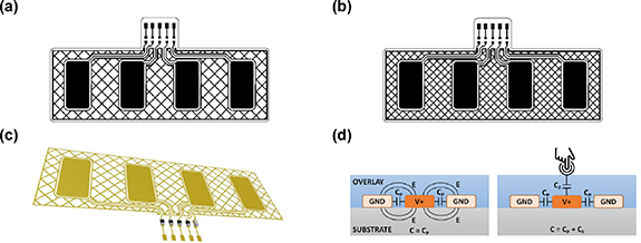
Figure 1. Capacitive sensors. (a) Design of the capacitive sensor with low-density ground net. (b) Design of the capacitive sensor with high-density ground net. (c) 3D design of the capacitive sensor with attached rigid electronic components. (d) Working principle of the mutual capacitive sensors.
Download figure:
Standard image High-resolution imageFor the design of the applied type of touch capacitive sensors, a second HGP is recommended under the capacitive touch electrodes to minimize possible external environmental interferences. However, to simplify the printing process and investigate the possibility of fabrication of the sensors in one single layer, the second ground electrode was eliminated. The final capacitive sensor (approximately 76 × 36 mm in size) consisted of four capacitive touch buttons and the HGP. Connected to the touch electrodes and the ground plane passive electronic components (resistances and capacitor) were integrated for impedance matching (figure 1(c)). Both designs were printed by means of inkjet printing and screen-printing processes over the different substrates.
3.1.2. Sensor manufacturing on different substrates
The capacitive sensors were fabricated by inkjet printing and screen printing on different substrates (PET, PC, PC/ABC) and the parameters of the printing process and drying conditions were optimized for each substrate and printing technique. Before that, the hydrophobicity of the obtained thermoplastics, PC, PC/ABS and the PET, was evaluated by contact angle measurements (see table 1).
Table 1. Contact angle measurement results.
| Substrate | Contact angle (°) | Error (°) | Behaviour |
|---|---|---|---|
| PET | 76.7 | 1.0 | Hydrophilic |
| PC | 96.9 | 3.3 | Hydrophobic |
| PC/ABS | 100.6 | 4.4 | Hydrophobic |
3.1.2.1. Inkjet printing
The printing on PET substrate resulted in formation of uniform layers with relatively high adhesion of the ink to the substrate. The printed layers on PC substrate showed a sheet resistance one order of magnitude higher (∼25 Ω sq−1) compared to those on the PET substrate (∼3 Ω sq−1). Moreover, the used silver ink seemed to interact with the PC substrate. At the other end, the printed sensors on PC/ABS substrate did not result conductive. Therefore, the morphology of these layers was further investigated by means of SEM.
According to contact angle results, PET showed to be hydrophilic with contact angle of 76.7 ± 1.0°, while PC and PC/ABS showed to be hydrophobic with contact angles of 96.6 ± 3.3° and 100.6 ± 4.4°, respectively (figure 2(a)). Thus, when using inkjet printing process, which is based on inks with polar solvents such as water or alcohols (specifically, triethylene glycol monomethyl ether for the Silverjet DGP-40LT-15C ink), the ink wettability is higher for PET than for other polymers. For this reason, the sensors printed on PET (figure 2(b)) shows better print quality and more accurate patterns than sensors printed on PC and PC/ABS.

Figure 2. (a) Contact angle measurements for the different substrates. (b) Inkjet-printed capacitive sensor with touch electrodes and demonstration of the flexibility of the printed sensor. (c) SEM images of the cross-section for the cold fractured printed sensors in all substrates. (d) Scheme of set-up for testing the capacitive sensors and detail of the attached rigid passive components and contacts for testing them.
Download figure:
Standard image High-resolution imageIn addition, solvent-based inks can chemically interact with the substrates. Attending to SEM results (figure 2(c)), three differentiated layers can be observed for inkjet printing on PC: polymer (bottom layer), polymer + Ag nanoparticles (1.3 μm, intermediate layer) and sintered Ag nanoparticles (2.3 μm, top layer), while only two layers are observed for PC/ABS substrates, the polymer and the sintered Ag nanoparticles (2.1 μm). Thus, it has to be highlighted that these two factors, the ink wettability on the substrates and the interaction between ink and thermoplastic substrates, reduces the quality of the inkjet-printed patterns when compared with the screen-printed ones, as it will be explained in the next section.
On the one hand, sensors printed on PET substrate show a low sheet resistance value (∼3 Ω sq−1) allowing the printing of completely functional as well as flexible capacitive touch sensors. The sensors printed on PC present high sheet resistance values, associated to a lower quality printing process that results in cracked Ag nanoparticle layer. However, this sample presents a homogenous and good quality intermediate layer also containing Ag nanoparticles in a lower content, leading to a less conductive sensor. Regarding PC/ABS substrate, no conductive tracks or electrodes are obtained, as no intermediate layer is obtained and, moreover, the top Ag nanoparticle layer is also cracked (figure 2(c)).
3.1.2.2. Screen printing
The sensors printed by means of screen printing resulted in improved uniformity of the printed layers with respect to inkjet-printed ones. Also, the sheet resistance of the screen-printed layers was significantly lower than the ones obtained by inkjet printing. In some cases, problems with the transfer of fine connection lines were observed. The screen printing also allows the fabrication of the capacitive sensors on PC and PC/ABS substrates without the sheet resistance being significantly affected (∼10−1−10−2 Ω sq−1), as well as maintaining high adhesion to all used polymer substrates. Only few defects were observed, such as incomplete ink transfer on the edges of the fine printed lines of the sensors connections or slight deformation of the printed structure due to the uneven surface of the prepared PC- and PC/ABS-based substrates. In general, all the screen-printed sensors showed higher thickness and roughness of the printed silver tracks in comparison to inkjet-printed ones, as it is presented in the SEM images of figure 2(c) (Ag layer thickness of 12 μm).
3.1.3. Test and results
Table 2 shows the main printing parameters and post-treatment conditions for each used polymeric substrate. For the characterization of the printed capacitive sensor demonstrators, measurements of impedance (resistance and capacity) between various contact points of the printed sensor circuit were performed. Figure 3(a) shows the ten different contact tracks used for the evaluation of the resistance. The evaluation was carried out for different combinations of substrates (PET, PC, PC/ABS), printing techniques (inkjet printing and screen printing) and also different design of HGP (light and dense) (figures 3(b) and (c)). The capacity was measured between the four touch buttons and the HGP for all named combinations as well (figures 3(d) and (e)). Figure 3(b) shows that the resistance values of the inkjet-printed tracks are significantly higher than the screen-printed ones (figure 3(c)).
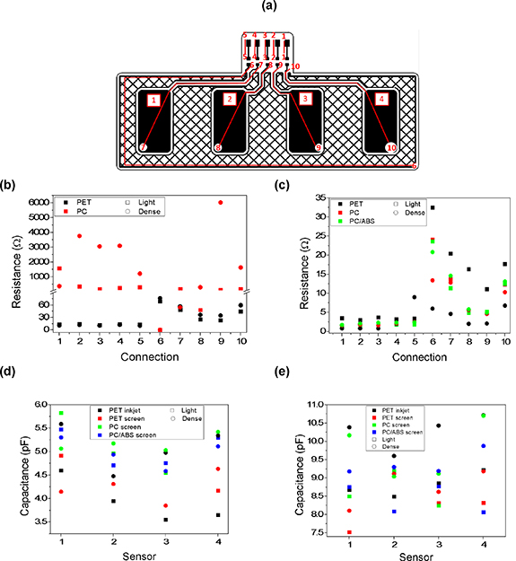
Figure 3. Resistance measurements between different testing points. (a) Contact points for the resistance and capacity measurements. Resistance measurements for (b) inkjet and (c) screen printing with light and dense mesh. Capacity measurements for (d) touch free and (e) touch active states of the capacitive buttons for light and dense mesh sensors.
Download figure:
Standard image High-resolution imageTable 2. Parameters of the printing process on different substrates.
| Printing technique | Substrate | Ink | Printing resolution/screen ruling | Head temperature | Number of printed layers | Substrate temperature | Curing temperature | Cure time |
|---|---|---|---|---|---|---|---|---|
| Inkjet | PET | Silverjet DGP-40LT-15C | 635 dpi | 45 °C | 3 | 50 °C | 120 °C | 30 min |
| PC-Elix | 35 °C | 2–3 | Room | 80 °C | 60 min | |||
| PC-Lexan | 35 °C | 2–3 | Room | 80 °C | 60 min | |||
| Screen printing | PET | Metalon® HPS-021LV | 90 threads cm−1 | — | 1 | Room | 120 °C | 30 min |
| PC-Elix | — | 1 | Room | 80 °C | 60 min | |||
| PC-Lexan | — | 1 | Room | 80 °C | 60 min |
The resistance of inkjet-printed tracks on PC and PC/ABS was in three orders of magnitude higher than in case of PET or did not result to be conductive at all (for the PC/ABS substrate). Therefore, these two combinations were excluded from further evaluation and the comparison of the two used techniques was based only on the inkjet-printed tracks on PET. The lower resistance values can also be related to the use of lower sintering temperatures, which could be potentially overcome by using alternative sintering methods such as photonic sintering. The resistance of the screen-printed sensors was is significantly lower than in the case of the inkjet-printed ones, which is related to the fact that the thickness of the screen-printed layers is significantly higher than for inkjet-printed ones, approximately in one order of magnitude. In the case of the screen-printed sensors, no significant difference in resistance values was found between the light and dense HGP, except for the PET substrate, where the lower resistance of dense HGP can be attributed to higher silver ink spreading on the PET substrate. The capacity of all evaluated sensors was ranging from ∼3.5 to ∼6 pF for touch free state and ∼7.5 to ∼11 pF for touch active state (figures 3(d) and (e)), respectively. In the following, further evaluation of the sensors was realized only with the light version of the HGP.
It is observed that the resistance values of inkjet-printed sensors are much more dispersed than in the case of screen-printing ones. Additionally, the resistance values of the screen-printed tracks are approximately one order of magnitude lower than the inkjet-printed ones. In general, all the screen-printed devices result to be more stable in terms of resistance variation and the used inks did not show any incompatibilities with the used substrates. On the contrary, the inkjet printing technique did not prove to be suitable for different flexible substrates. Using the PET substrate, functional devices have been achieved, however, when the PC and PC/ABS substrates were used, the inkjet-printed devices did not result to be functional. Additionally, the inkjet-printed sensors require various repeated prints to achieve sufficiently low sheet resistance, which extends the manufacturing, in particular when printing larger tracks or circuits. On the other hand, inkjet printing allows a quick variation of the printed design, whereas screen printing requires the fabrication of a new stencil, which is also time consuming.
Based on the printing experiments and to ensure sufficient repeatability of the sensor printing process, the separation between the printed tracks should not be lower than 500 μm and the minimum recommended width of the printed lines should not exceed 200 μm.
Regarding capacity, a certain dispersion of the experimentally measured data was observed. Nevertheless, in all cases the measured capacity values were in the range of picofarads (pF). To evaluate the functionality of the printed sensors, for the processing of the measurement it was necessary to mount four resistances with 560 Ω value to adjust the resulting impedance of the printed tracks of the circuit and to be able to connect the capacitive sensors to the evaluation microprocessor and one 2.2 nF capacitor to filter the noise between GND, the capacitive bottoms and the processing (figure 2(d)).
The characterization of the printed capacitive sensors was realized with the sensors connected to the evaluation electronics equipped with Cypress CapSense microprocessor. The performed measurements have not shown any significant differences in the sensitivity of the capacitive sensor response, when using the high- or low-density HGP.
Figure 4 shows the results of the capacitive sensor response as a function of the applied current frequency. It can be observed how the capacitance decreases with increasing frequency, but the sensors can operate in a stable way in the range from 900 Hz to 100 kHz. The sensors printed on PET showed slightly higher capacitive response in comparison to those ones deposited on PC and PC/ABS substrates. An abnormal behaviour has been observed at around 8 kHz, which is attributed to 'band stop filter', which attenuates certain frequencies and therefore this frequency and near frequencies to 8 kHz should be avoided (e.g. by limitation of the current frequency to 1 kHz). After processing and digital discretization, an increase of approximately 150× was observed from the touch free to the touch condition.
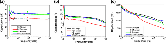
Figure 4. Results of the capacitive response of the tested sensors on different substrates printed by inkjet and screen printing. (a) Touch free state (without touch). (b) Touch active state of the capacitive bottom. (c) Touch active state of the capacitive bottom including the HGP.
Download figure:
Standard image High-resolution imageFigure 5 shows the capacitive response (represented by the normalized amplitude after the digital signal processing) at a frequency of 1 kHz of the capacitive sensors deposited on different used substrates. All fabricated sensors were tested by a sequence of multiple touches with different intensity of touch and time of finger contact with the sensors (first, longer pulses of approximately 5 ms and then short ones of 1 ms) to verify both the sensor sensitivity to applied finger force and the time response. In the case of PET substrate, the two employed printing techniques are compared as well. It is observed in figure 5 that in all cases the sensors are sensitive to the different applied touch times and intensities. By using the larger touch pulses, practically no signal noise was detected. However, very short touch pulses may induce some signal noise. There was no significant difference between the two used printing techniques. The screen-printed sensors worked correctly on all evaluated substrates. The possible baseline shifts can be attributed to slight movements during the sensor touching.

Figure 5. Results of the tactile detection of sensors with the light HGP design on various substrates. (a) PET substrate and manufactured by inkjet printing. (b) PET substrate and manufactured by screen printing. (c) P substrate and manufactured with screen printing. (d) PC/ABS substrate and manufactured with screen printing.
Download figure:
Standard image High-resolution image3.2. Integrated capacitive sensor with illumination circuit
3.2.1. Design
The developed capacitive sensors integrate only simple passive electronic components, such as resistances and capacitor. To deeper evaluate the feasibility of the fabrication of more complex hybrid electronic circuits, a new design integrating several LEDs and a driver for the control of their current source was prepared, the driver being an integrated circuit with encapsulated 16 pins.
Due to the complexity of the circuit with the integrated driver, it was not suitable to realize the circuit with only one layer of the printed tracks. To realize all the necessary interconnections of different circuit components, it was essential to cross the printed circuit tracks and therefore divide the circuit into three individual layers printed one on top of each other (bottom conductive layer, intermediate dielectric insulation layer and top conductive layer). Figure 6 shows the design of the printed individual layers and the 3D visualization of the illumination circuit with integrated components.
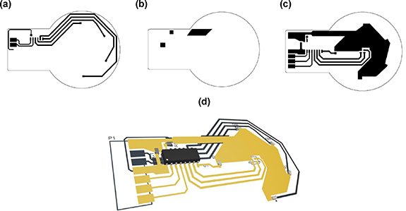
Figure 6. (a) Bottom conductor layer. (b) Dielectric layer. (c) Top conductor layer. (d) 3D design of the printed illumination circuit with integrated rigid components.
Download figure:
Standard image High-resolution imageThe electronic design software used for the design of the electronic circuit, Altium, already allows the overcrossing of conductive tracks by means of dielectric insulation patches, which in practice results in a multilayer design. As shown in figure 6, the area for the connection of the LEDs was maximized to diminish the resistance of the printed tracks used for the power supply of the LEDs, as well as to maximize the heat dissipation area.
3.2.2. Manufacturing and mounting
The printed illumination circuit was divided into three printing steps, for the printing of each layer of the design (bottom conductor, dielectric and top conductor). The illumination circuit was printed on PET, PC and PC/ABS.
Each printed layer needed an intermediate drying step of 80 °C during 5 min to avoid the deformation of the used polymeric substrates and finally the whole three layer stack was cured at 120 °C during 20 min to finalize the sintering of the printed layers on PET. In the case of the PC and PC/ABS substrates, due their lower temperature resistance, the sintering temperature was reduced to 100 °C.
Based on the more promising results from the experiments realized during the capacitive sensor manufacturing with screen printing, the illumination circuit was fabricated only by screen printing. To ensure a robust separation of the bottom and top conductor layer, based on the preliminary tests, it was necessary to deposit at least two consecutive layers of the dielectric.
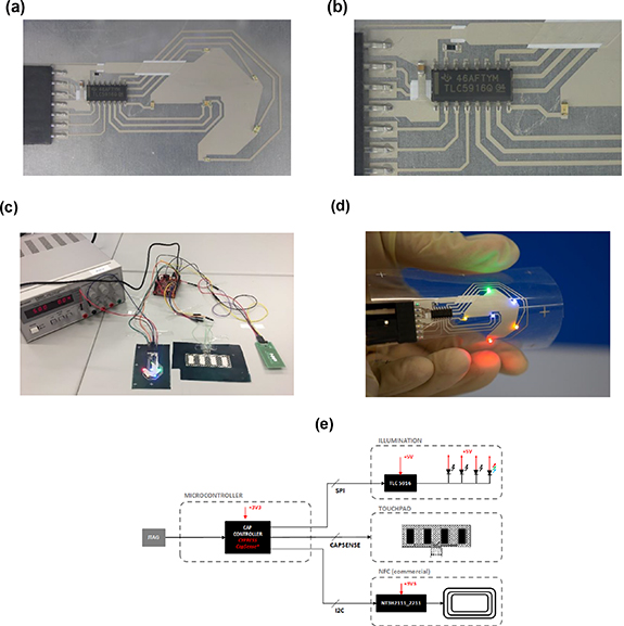
The printed circuit was later integrated with ten rigid components such as red, blue, yellow, green and RGB colour LEDs, power driver, capacitor, and resistance. Where, the LEDs used were 150120RS75000, 150120BS75000, 150120BS75000, 150120GS75000, and 156120M173000; the power driver was the TLC5916 with a current limitation resistance of 820 Ω and a decoupling capacitor of 0.1 μF. The pick and place process of these components was manual using a commercial conductive adhesive (figure 7(a)). Afterwards, the adhesive was cured at 110 °C during 40 min.
Figure 7. Final integration of all printed tested components. (a) Scheme of the complete set-up of capacitive sensors with illumination circuit. (b) Detail of the integrated attached components on the illumination circuit. (c) Working set of capacitive sensors with illumination circuit. (d) Demonstration of flexibility of the printed illumination circuit. (e) Scheme of the final complete set-up with illumination circuit controlled by means of capacitive sensors.
Download figure:
Standard image High-resolution image
3.2.3. Test and results
To evaluate the functionality of both printed demonstrators, these were connected together and then also to the evaluation electronics used previously for the assessment of the capacitive sensors (figure 7). The Cypress evaluation board CY8CKIT-040 with the microprocessor PSoC 4000 Arm Cortex-M0 (figure 7(b)) was used for the evaluation was programmed to control the illumination circuit by means of the printed capacitive sensors (scheme in figure 7(e)). Parameters such as the light intensity and the illumination sequence of the individual LEDs were controlled by the touch bottoms of the capacitive sensors, as well. The results are presented both in figures 7(c) and (d) and the corresponding video provided as supporting information (available online at stacks.iop.org/FPE/6/015004/mmedia).
4. Conclusions
The present work reports on mutual flexible capacitive sensors fabricated by means of both screen and inkjet printing on different substrates, including standard PET and injection-moulding compatible PC and PC/ABS-based thermoplastics. Additionally, the produced capacitive sensors were integrated with a printed flexible illumination circuit to control different LEDs with programmed illumination sequences. The capacity of all tested sensor designs ranged from ∼3.5 to ∼6 pF in touch free state and from ∼7.5 to ∼11 pF in touch active state. The capacitive sensors operated in a stable way in the frequency range from 900 Hz to 100 kHz. The HGP design did not have a significant influence on the sensor response and therefore the sensors were finally evaluated only with light HGP design. The inkjet-printed sensor showed generally higher and more dispersed resistance values (up to kΩ range), whereas the screen-printed ones showed significantly lower (of the order of tens of Ω) and more homogeneous resistance values. It was observed that the used silver ink interacted with PC and PC/ABS substrates, which resulted in an increase of the resistance of the printed tracks on PC and on non-continuous printed tracks on PC/ABS. Therefore, screen printing showed to be more suitable for PC and PC/ABS substrates, whereas both inkjet and screen printing can be used on PET standard substrate. The present work open the way for the development of injection-moulded electronic components and to the evaluation of their performance as a function of varying injection-moulding parameters.
Acknowledgments
The authors thank funding from the Basque Government Industry and Education Department under the ELKARTEK, HAZITEK and PIBA (PIBA-2018-06) programs, respectively.