

Abstract
The topological state that emerges at the surface of a topological insulator (TI) and at the TI-substrate interface are studied in metal–hBN–Bi2Se3 capacitors. By measuring the RF admittance of the capacitors versus gate voltage, we extract the compressibility of the Dirac state located at a gated TI surface. We show that even in the presence of an ungated surface that hosts a trivial electron accumulation layer, the other gated surface always exhibits an ambipolar effect in the quantum capacitance. We succeed in determining the velocity of surface Dirac fermions in two devices, one with a passivated surface and the other with a free surface that hosts trivial states. Our results demonstrate the potential of RF quantum capacitance techniques to probe surface states of systems in the presence of a parasitic density-of-states.
Export citation and abstract BibTeX RIS

Original content from this work may be used under the terms of the Creative Commons Attribution 3.0 licence. Any further distribution of this work must maintain attribution to the author(s) and the title of the work, journal citation and DOI.
Radio frequency (RF) transport has been widely used to characterize various low-dimensional systems including graphene [1–8] and to detect and manipulate edge states via interferometric techniques [9–11]. Such techniques have recently gained importance in the context of the detection of coherent and topological states that are useful for quantum computing [9, 12]. In a non-metallic 2D material, a simple two terminal metal–insulator-2D material capacitor device allows one to directly probe the density-of-states (quantum capacitance) and the channel resistance of the material, without the need for a magnetic field. Previous studies on graphene have successfully used this device geometry to characterize the scattering dynamics of charge carriers and electron-phonon interactions [1].
RF capacitance measurements in the two terminal device architecture have also been performed on topological insulators (TIs) [13–15]. In contrast with graphene, three-dimensional TIs have more complex dielectric properties. Bi2Se3—a prototypical TI—has a large bulk energy gap (200 meV) with two Dirac states bound to each surface. RF capacitance can be used to probe the quantum capacitance (cq), the conductivity of the material and the inter-surface dielectric coupling via the bulk as demonstrated by our recent work [14, 15]. The quantum capacitance  is of particular interest since it is proportional to the material's electronic compressibility
  via
via  For the Dirac fermions of TIs:

Here  is the Fermi energy with respect to the Dirac point,
  is the Dirac velocity and
  and
and  have their usual meaning.
In this work, we investigate the quantum capacitance of topological surface states and interface states in metal–insulator-topological insulator capacitor devices (MITI-CAP) having two different architectures. In the first, a top-gate is used to probe the top surface quantum capacitance while in the second a bottom gate probes the quantum capacitance of the substrate-TI interface. We build on the recently demonstrated process that uses physical vapor deposition (PVD) combined with the dry transfer of a hexagonal boron nitride layer to design and process MITI-CAP devices [15, 16]. A major advantage of such devices is the use of hBN to apply electric fields exceeding 1 V nm−1 and tune the Fermi energy through the surface Dirac point of Bi2Se3. We successfully achieve this for both the top surface and bottom interface states of Bi2Se3 and measure the capacitance and channel resistance of MITI-CAPs up to 10 GHz in both cases. The devices allow us to measure the velocity of topological Dirac fermions at the gated surface. We compare measurements from two devices with and without an hBN passivation layer. The importance of this passivation layer in preventing surface impurities from yielding an accumulation layer is established. We also demonstrate the viability of RF compressibility measurements to probe surface states even in the presence of the accumulation layer.
Top-gated MITI-CAPs are processed by first synthesizing Bi2Se3 on exfoliated hBN using PVD in figure 1(a) and then placing a second hBN layer on top using the well-established dry-transfer technique [17, 18]. We obtain an hBN–Bi2Se3–hBN heterostructure shown in figure 1(b) [15, 16]. For the bottom gated MITI-CAP, we first pattern a 40 nm Pt gate electrode and then dry transfer an hBN layer on top the Pt gate (figure 1(c)). This hBN layer then serves as a substrate for the synthesis of Bi2Se3 by PVD. A seen in figure 1(d), Bi2Se3 nucleates faster on the Pt/hBN stack than on the SiO2 substrates, leaving a continuous layer deposited to form a Pt–hBN–Bi2Se3 MITI stack. All samples are characterized using atomic force microscopy and Raman spectroscopy. The top-gated MITI-CAPs were studied in detail in our previous work [15]. An atomic force microscope (AFM) height profile taken on a bottom gated MITI-CAP is shown in figure 1(e). By performing AFM on the hBN layer before the growth and on the hBN–Bi2Se3 after the growth, we can extract the thickness of the hBN layer (8.3 ± 0.3 nm) and that of Bi2Se3 (8 quintuple layers). Note that the typical roughness of our Bi2Se3 layers is 1 quintuple layer (±1QL) as can be seen in figure 1(e). Figure 1(f) shows Raman spectra taken from both samples shown in figure 1. The three characteristic phonon peaks of Bi2Se3 [19] are observed and confirm the successful synthesis of high-quality material on the hBN surface.

Figure 1. (a) Bi2Se3 flake synthesized by PVD on hBN. (b) Flake shown in (a) with hBN dry-transferred on top. (c) Pt bottom gate with hBN flake dry-transferred on top. (d) Bi2Se3 synthesized by PVD on the hBN/Pt stack. (e) Atomic force microscope data for the flake shown in (d) before (blue) and after (red) the synthesis of Bi2Se3. (f) Micro-Raman spectra taken on both samples at room temperatures with a green 514 nm laser excitation. (QL: quintuple layer).
Download figure:
Standard image High-resolution imageA top-gated MITI-CAP device (CAP1) is finished in a single electron beam lithography step followed by the deposition of a Ti(5 nm)/Au(200 nm) metal bilayer to form the gate, drain and waveguide [15]. A finished device is shown in figure 2(a). The same method is used to deposit the drain and waveguide for the case of the bottom-gated MITI-CAP (CAP2). They are patterned on the free top surface of the Bi2Se3 by e-beam lithography followed by the deposition of Ti(5 nm)/Au(200 nm). Lastly, in order to ensure that the Bi2Se3 is electrically separated from the Pt gate in CAP2, we etch a window in the TI near the gate. A finished device obtained using this hybrid dry-transfer/PVD process in shown in figure 2(b) and its insets. The main difference between CAP1 and CAP2 is the location of the gate. In CAP1 illustrated in figure 2(c) the gate controls the chemical potential of the top surface and the Bi2Se3 is sandwiched between hBN layers. In CAP2, shown in figure 2(d), the gate controls the bottom surface chemical potential and the top surface is open to air. In both cases a distributed RC model can be used to model the RF response (figure 2(e)). The device dimensions are shown in table 1.

Figure 2. Optical microscopy of the two devices investigated in this work (a) CAP1 and (b) CAP2. Sketch of the cross-section of (c) CAP1 and (d) CAP2. D and G label the drain and gate contacts respectively. (e) Circuit diagram of the distributed RC model used to analyze the RF response of both devices.
Download figure:
Standard image High-resolution imageTable 1. Device parameters of CAP1 and CAP2.
| Device | CAP1 | CAP2 |
|---|---|---|
| Gate configuration | Top gate | Bottom gate |
| Structure | hBN–Bi2Se3–hBN-Gate | Gate–hBN–Bi2Se3 |
| L × W (μm × μm) | 4.3 × 12.8 | 20 × 3 |
| hBN thickness | 8.0 nm (12 bilayers) | 8.3 ± 0.2 nm (12–13 bilayers) |
| Bi2Se3 thickness (±1QL) | 8QL | 8QL |
| cg (fF μm−2) | 2.25 ± 0.02 | 3.41 ± 0.05 |
| Δεf (at gated Dirac point) | 195 meV | 220 meV |

|
5.2 × 10⁵ m s−1 | 4.9 × 10⁵ m s−1 |
 (fF μm−2) (fF μm−2) |
110 | 110 |
 (fF μm−2) (fF μm−2) |
25–35 | 50–85 |
In what follows, we will focus on the measurement of the quantum capacitance of CAP1 and CAP2 and their comparison. A two-probe setup connected to a network analyzer allows us to determine the S-parameters of the capacitors versus frequency up to 10 GHz. A standard short-open-load-through calibration is performed before each measurement at 10 K. The experiment is performed with one probe (ground) connected to the drain (D) while RF and DC are simultaneously connected to the gate (G) via a bias-T. The frequency is swept between 70 kHz and 10 GHz at constant DC gate voltage. The S-parameters are experimentally extracted at different frequencies and converted to admittance Y. A de-embedding routine is then performed to disentangle the capacitive and resistive components of a through-line and a dummy device consisting of an identical gate and drain geometry without the sample in between [20]. This procedure is identical to that used in our previous works [1, 13, 14]. It is repeated for different gate voltages (0 to −7 V).
The real and imaginary parts of Y obtained from CAP2 are plotted in figure 3(a). Those of CAP1 are shown in our previous work [15]. The admittance agrees well with that expected for a 1D distributed RC model [1] with a series contact resistance (figure 2(e)) 

where

Here,  is the frequency.
  is the channel conductance (in Ω−1) and c is the total device capacitance per unit area. By curve fitting the real and imaginary parts of Y we can obtain three fit parameters shown in equation (2),
  , c and the contact resistance
  The latter is fixed to 150 Ω. Allowing it to vary yields variations that are negligible within the uncertainty of the experiment.

Figure 3. Real (red) and imaginary (blue) parts of the admittance of CAP2 versus frequency up to 10 GHz at different gate voltage between 0 and −7 V. Green curves are theoretical fits using the distributed RC model. (b) Square resistance and (c) capacitance versus gate voltage at 10 K. In (b) and (c) filled and open symbols denote the parameters of CAP1 and CAP2 respectively.
Download figure:
Standard image High-resolution imageThe channel square resistance Rs = ( ) and capacitance per unit area
  for both devices are shown in figures 3(b), (c) respectively.
  and
and  are respectively the length and width of the capacitor. While a clear capacitance minimum is observed in both CAP1 and CAP2, suggesting successful tuning through the Dirac node, the channel resistance does not exhibit a maximum, indicating the presence of additional conducting channels in the samples that are not well coupled to the gate. The analysis of the quantum capacitance sheds further light on this issue. The data shown in figure 3(c) can be used to extract the quantum capacitance
  From the capacitance per unit area, we extract
  using
using  The geometric capacitance
  for both devices is shown in table 1. Notice that
  is smaller in CAP1 since the gated surface is exposed to air before the hBN is transferred in top. This introduces impurities—possibly an air or vacuum layer between the hBN and Bi2Se3—and reduces the dielectric constant of the gate dielectric. In CAP2,
  yields the dielectric constant of hBN that is recognized in the literature (
 ) [7, 21, 22]. The data in figure 3(c) also allows us to extract the chemical potential at the gated surface using the Berglund integral [6]:
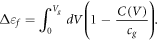
We are thus able to extract how the quantum capacitance—a direct measurement of the density-of-states—varies with the surface chemical potential ( ) relative to its position at zero gate voltage. This is shown in figure 4(a). A linear fit is performed in figure 4(a) to determine the Dirac velocity using equation (1). We find 5.2 × 10⁵ m s−1 and 4.9 × 10⁵ m s−1 for CAP1 and CAP2 respectively in agreement with previous studies [23, 24]. The velocity of Dirac particles is thus identical for a TI surface and the TI/hBN interface within our experimental uncertainty.

Figure 4. (a) Quantum capacitance versus Fermi energy for CAP1 (full circles) and CAP2 (empty circles). Red lines are curve fits using equation (1). Band alignment diagram of CAP1 (b) and CAP2 (c) with the ungated surface offset in energy with respect to the gated surface. G marks the location of the gate.
Download figure:
Standard image High-resolution image
An important feature of the figure 4(a) is the finite residual density-of-states that is reproducibly observed in both samples. It is easy to rule out calibration imperfections and random experimental error as the origin of this finite density-of-states at zero chemical potential. While the quantum capacitance of ideal Dirac cones is never zero at the Dirac node, previous measurements on graphene have observed order of magnitude lower values [25]. Additionally, even if the quantitative value of cmin is highly sensitive to the value of cg, cmin remains significant within the experimental error bars associated with cg (see table 1). It is thus obvious that cmin is not an experimental artifact.
Since the bottom surface is not efficiently coupled to the gate, our devices always result in a chemical potential offset between the two surfaces. We have previously analyzed the capacitance minimum in Bi2Se3 (in CAP1) and have attributed it to the capacitive coupling through the depleted bulk of the ungated surface with the gated surface due to the large permittivity of Bi2Se3 [15]. When the chemical potential is at the Dirac point at the top surface and the bulk is depleted, the ungated bottom surface is capacitively coupled through the insulating bulk. In CAP1, this yields:

With
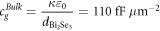
Here the dielectric constant  [26–29] and
 Using equation (1) we can show that this corresponds to a Fermi energy of about 170 meV above the Dirac point at the bottom ungated surface.
It is interesting to note that the offset observed in CAP2 with the top surface exposed to air, is larger than the one observed in CAP1 with the passivated surface, even within experimental uncertainty. We find  for the upper bound of the uncertainty in cg (see table 1). If we assume an ungated surface coupled to the gated surface of CAP2 through an insulating bulk with we can compute
  using:
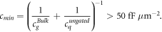
With  one needs
  From equation (1), this corresponds to a Fermi energy in excess of 390 meV above the Dirac point if only Dirac fermions are assumed to populate the ungated surface. In Bi2Se3, the Dirac point is about 200 meV below the conduction band [23, 24], therefore a conduction level has to be populated at the ungated surface. We thus have to consider the presence of a surface accumulation layer to account for
  in CAP2. The quantum capacitance from this layer is given by
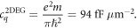
Here  is the effective mass of the 2DEG taken equal to that of the bulk conduction band of Bi2Se3 [30]. With
  determined above,
  can be greater than
  Note that it is obviously possible to have contribution from both a Dirac surface states and a 2DEG yielding
  However, it is not straightforward to determine each independently given the uncertainty on
The parameters extracted from the experiment for CAP1 and CAP2 are summarized in table 1. From the analysis of figure 4(a), we thus conclude that in CAP1, when the top gated surface state is charge neutral and the bulk is depleted, the bottom ungated topological interface state is populated with a Fermi energy about 170 meV above its Dirac point (figure 4(b)). In the case of CAP2, when the bottom gated interface state is charge neutral, the bare top surface is also populated by an electron accumulation layer (figure 4(c)). Without this accumulation layer, the finite capacitance minimum cannot be accounted for in CAP2.
Differences in sample quality resulting from growth might also explain  being larger for CAP2. Results from three different growths were, however, analyzed in our previous work and the quantum capacitance in the trilayers hBN–Bi2Se3–hBN consistently reached values smaller than 35
  [15]. All these observations suggest that the presence of the bare surface exposed to atmosphere likely results in the accumulation layer responsible for the additional capacitance observed in CAP2. Note that surface and interface roughness can also yield a finite capacitance by causing a spatial inhomogeneity of the position of the Dirac point in energy. However, this would require the disorder potential close to 100 meV to account for the observed
  and would not entirely explain the differences observed by comparing devices [31].
The reason why the resistance (figure 3(b)) does not reach a maximum at the quantum capacitance minimum in both CAP1 and CAP2 is also likely due to these multiple contributions from the ungated surfaces. In CAP1, the top and bottom surface are both conducting, but the bottom surface retains a large number of carriers when the top surface is neutral. The same situation arises in CAP2, but the presence of the trivial accumulation layer likely yields a weaker the modulation of the resistance versus gate voltage as seen in figure 2(b). This observation can be qualitatively explained by the fact that a parabolic dispersing 2DEG has a flat density of states (versus Fermi energy). However, a quantitative understanding of the behavior of the resistivity requires further studies.
Lastly, note that previous photoemission and transport measurements [27, 32] have reported the observation of a surface 2DEG coexisting with the topological state. Additional measurements also showed that the Dirac points at opposite surfaces can be offset in energy by several 100 meV [33]. Our results agree with those observations and suggest that this 2DEG can have a parasitic impact on Dirac transport if left un-passivated or un-gated. Even under a strong electric field (0.75 V nm−1) applied to one surface of a TI and likely strong enough to deplete the bulk bands, an accumulation layer at the opposite ungated surface can remain difficult to alleviate if that surface has been exposed to air. The hBN layer likely prevents the formation of the accumulation layer by protecting the ungated surface during the device processing steps. Interestingly, even though the conductivity of the TI remains dominated by transport from carriers at the ungated surface and interfacial layer, the quantum capacitance of the Dirac cones at the gated surface can still be reliably measured.
In summary, we have measured the RF quantum capacitance and channel resistance of two MITI-CAP devices. The quantum capacitance shows a behavior reminiscent of Dirac fermions characteristic of the surfaces of Bi2Se3. Our measurements demonstrate the importance of passivating and gating away charges from surfaces exposed to air to achieve surface conduction, in the addition to optimizing the bulk of Bi2Se3 to become insulating. Several recent developments have yielded promising results in this direction [16, 34, 35]. Most importantly, our work shows that the RF compressibility remains a viable technique to study the fundamental dielectric properties of topological surfaces in the presence of a finite and small parasitic density-of-states from other bands. As long as a gate voltage can be reliably used to locally tune the Fermi energy across the Dirac point, the compressibility of the Dirac state can be measured. This fact becomes particularly important when considering metallic systems such as three-dimensional Weyl semimetals with Fermi arcs at their surfaces [36, 37].
Acknowledgments
We acknowledge Michael Rosticher for valuable assistance with cleanroom equipment and Pascal Morfin for his assistance with the growth setup. We also acknowledge discussions with H Graef BAA, JD and TW acknowledge funding from ANR-LabEx grant ENS-ICFP ANR-10-LABX-0010/ANR-10-IDEX-0001-02PSL. JD was partially supported by the Northeastern University Coop fellowship. KW and TT acknowledge support from the Elemental Strategy Initiative conducted by the MEXT, Japan, A3 Foresight by JSPS and the CREST (JPMJCR15F3), JST.