

Abstract
Monolayer tungsten disulfide (WS2) has recently attracted a great deal of interest as a promising material for advanced electronic and optoelectronic devices such as photodetectors, modulators, and sensors. Since these devices can be integrated in a silicon (Si) chip via back-end-of-line (BEOL) processes, the stability of monolayer WS2 in BEOL fabrication conditions should be studied. In this work, the thermal stability of monolayer single-crystal WS2 at typical BEOL conditions is investigated; namely (a) heating temperature of 300 °C, (b) pressures in the medium- (10−3 mbar) and high- (10−8 mbar) vacuum range; (c) heating times from 30 minutes to 20 hours. Structural, optical and chemical analyses of WS2 are performed via scanning electron microscopy, Raman spectroscopy, photoluminescence and X-ray photoelectron spectroscopy. It is found that monolayer single-crystal WS2 is intrinsically stable at these temperature and pressures, even after 20 h of thermal treatment. The thermal stability of WS2 is also preserved after exposure to low-current electron beam (12 pA) or low-fluence laser (0.9 mJ μm−2), while higher laser fluencies cause photo-activated degradation upon thermal treatment. These results are instrumental to define fabrication and inline monitoring procedures that allow the integration of WS2 in device fabrication flows without compromising the material quality.
Export citation and abstract BibTeX RIS

Original content from this work may be used under the terms of the Creative Commons Attribution 4.0 license. Any further distribution of this work must maintain attribution to the author(s) and the title of the work, journal citation and DOI.
1. Introduction
Monolayer transition metal dichalcogenides (TMDs) have attracted a great deal of interest due to their excellent electrical and optical properties [1–8]: because of their semiconducting nature, TMDs allow to overcome the shortcomings of zero-bandgap graphene, showing attractive potential for constructing digital circuits [9, 10] and next generation light-emitting devices [11, 12]. In addition to the large range of available bandgaps of pristine S-, Se- and Te-based TMDs [13–17], the facile intermixing in different alloys [18–22] and stacking in heterostructures [23–25] give way to virtually infinite possibilities of electronic and optical properties engineering. Moreover, the integration of large-area semiconducting TMDs with existing complementary metal oxide silicon (CMOS) platforms promises fast advances in electronic and photonic technologies [26–29]. In CMOS fabrication procedures, silicon (Si) chips are processed with a series of steps grouped into two fabrication portions known as front-end-of-line (FEOL) and back-end-of-line (BEOL) [30]. In the FEOL individual devices are patterned on the Si chips, while in the BEOL these devices are interconnected with each other and with the outside world. Similarly to graphene, TMDs can be monolithically integrated with well-established CMOS BEOL [28]. Indeed, TMDs-Si chips have already been reported for a number of applications [29, 31–35]. This compatibility gives to TMDs a great advantage in terms of process optimization and cost reductions with respect to other 'beyond-CMOS' candidates, such as III–V semiconductors or Ge, in which indirect integration with Si chips is much more challenging [36].
Monolayer tungsten disulfide (WS2) has attracted large interest due to its unique properties, such as large spin–orbit splitting at the valence band K-point (462 meV) [37] and high emission quantum yield [38]. By manipulating the spin and valley degrees of freedom of WS2, novel spintronic and valleytronic devices can be developed [39, 40]. WS2 also shows remarkably large light–matter interaction with high exciton binding energy (BE) (700 meV) [41] that, together with the possibility to grow large-area monolayer, has made WS2 an enticing candidate for applications in electronics [29], optoelectronics [42] and photonics [34, 43]. Indeed, some examples of WS2-based devices fabricated in typical CMOS BEOL conditions have already been reported: Yang et al [34] have demonstrated a WS2-based all-optical modulator fully integrated with typical CMOS Si3N4 waveguides to modulate a 532 nm pump light source. Moreover, a fully CMOS-compatible graphene-hBN-WS2 metal–insulator–semiconductor transistor showing ambipolar behavior has also been recently reported [35]. These early results confirm that the optimization of WS2–Si chips can be boosted by employing already-optimized CMOS BEOL fabrication steps, rather than implementing a completely new protocol.
In light of the great applicative potential of monolayer WS2, its stability under typical BEOL processing conditions needs to be assessed to devise correct handling and fabrication procedures. To date, it has been reported that —under ambient conditions— monolayer WS2 slowly reacts with environmental oxygen and fully degrades within 1 year [44]. Instead, if the environmental aging takes place at higher temperatures, the degradation accelerates [45, 46]. Rong et al [46] found that polycrystalline WS2 monolayer starts to degrade in static air after 90 minutes at 250 °C and after only 20 minutes at 380 °C [46]. Additionally, it has been observed that the substrate on which WS2 is grown can play a role in either boosting [47] or hindering [48] the oxidation of WS2, depending on the electron transfer between WS2 and the substrate [47]. Experimental and theoretical works agree on the fact that WS2 degradation initiates at defective sites (i.e. sulfur vacancies, grain boundaries, edges) and it is due to the oxidation of WS2 when interacting with environmental oxide species.
The abovementioned studies shed light on the stability and the degradation mechanism of WS2 in air, at either room temperature or upon annealing. However, typical BEOL processes, such as deposition of dielectrics, evaporation of metal contacts and post-deposition annealings, are carried out at temperatures between 300 °C and 400 °C and base pressures that range from a few mTorr (∼10−3 mbar) to 10−6 mTorr (∼10−9 mbar) [49–53]. Therefore, the results already present in literature do not explore the stability of monolayer WS2 under BEOL conditions. To fill this gap, in this work monolayer WS2 is exposed to standardized conditions that are representative of typical BEOL fabrication protocols [28, 54, 55], and its structural, chemical and optical properties are studied. In addition to the fabrication steps, BEOL procedures also include inline monitoring of the material quality by adopting fast, non-contact methods, such as optical and scanning electron microscopies (SEM) and Raman and photoluminescence (PL) spectroscopies [27]. A fast, non-destructive microscopic technique is indeed necessary to evaluate the morphological properties of the fabricated sample with suitable resolution and without any required sample preparation that would destroy the device. In this sense, both optical and SEM imaging can be good candidates, depending on the size of the single-crystals. Recently, it has been suggested that the degradation of WS2 monolayer at room temperature can be photo-induced by exposure to focused light and that the rate of this phenomenon is strictly dependent on the power of the light used [56, 57]. Hence, before integrating WS2 in BEOL flows, the compatibility of WS2 to intermediate characterization steps involving techniques based on focused lights, such as Raman and PL spectroscopies, should be first demonstrated and the optimal conditions, needed to preserve the quality of the material, found.
In this work, monolayer WS2 was epitaxially grown on hydrogen-etched sapphire substrate (α-Al2O3 (0001)) via low-pressure chemical vapor deposition (LP-CVD) and its thermal stability was evaluated at typical BEOL conditions (300 °C and base pressure of 10−3 mbar and 10−8 mbar). The morphological, structural and optical modifications upon annealing were evaluated and it was found that freshly grown WS2 monolayer is intrinsically stable in these conditions even for long annealing times (up to 20 hours). Furthermore, the stability of WS2 was investigated at 300 °C and medium-vacuum (1 × 10⁻³ mbar) after exposure to commonly used characterization techniques, i.e. SEM, X-ray photoemission spectroscopy (XPS), Raman and PL spectroscopies. It was observed that SEM (e-beam current 12 pA) has no effect on the stability of WS2 at 300 °C, while the exposure to laser can trigger the degradation of WS2. In particular, if WS2 is exposed to a 532 nm laser with a fluence of 9.4 mJ μm−2 (laser power 730 μW), the morphological and optical properties of WS2 rapidly degrade upon annealing at 300 °C. If the laser fluence is below a threshold of 0.9 mJ μm−2 (laser power 73 μW), instead, no oxidation is initiated and monolayer WS2 remains stable at 300 °C for several hours. These results are instrumental not only for future successful integration of monolayer WS2 in BEOL fabrications, but also to avoid sample damaging when performing fundamental analyses that rely on laser adoption and sample annealing.
2. Experimental methods
2.1. Sample preparation
The substrates used for CVD growth of monolayer WS2 were dice cut from c-axis, HEMCOR single-crystal, sapphire α-Al2O3 (0001) wafers supplied by Alfa Aesar (Germany). Before WS2 growth, sapphire substrates were cleaned via sonication in acetone, isopropanol, and de-ionized (DI) water, then immersed in piranha solution (1:3, H2O2:H2SO4) for 15 min and finally washed in DI water. Subsequently, the dice were etched in hydrogen atmosphere as described in [58] to remove polishing scratches and reveal atomic steps.
The etched sapphire substrate was then directly loaded in the CVD reactor for the growth of monolayer WS2 via LP-CVD. Tungsten trioxide (WO3, powder, Sigma Aldrich, 99.995%) and sulfur (S, pellets, Sigma Aldrich, 99.998%) were used as solid precursors. The process was performed within a 2.5 inches horizontal hot-wall furnace (Lenton PTF): the furnace comprises a central hot zone (growth zone), where a crucible loaded with WO3 powder was placed 3 cm away from the growth substrate, and an inlet zone, where the S powder was positioned and separately heated by a resistive belt at 120 °C. Temperature in the growth zone was concurrently ramped-up to 930 °C, at a chamber pressure of ∼5 × 10⁻² mbar. During the growth Argon was adopted as carrier gas, as described in [37, 59].
2.2. WS2 thermal annealing
Medium-vacuum thermal annealing of WS2 was performed in a hot-wall CVD quartz tube reactor, while high-vacuum annealing was carried out in an ultra-high-vacuum (UHV) chamber used for XPS measurements. In the CVD reactor, the annealings were performed at a temperature of 300 °C, a base pressure of 1 × 10⁻³ mbar and a temperature ramp-up rate of 5 °C min−1. The medium-vacuum annealing was carried out either in a continuative manner up to 10 h or by extracting and characterizing the sample after each annealing step. The high-vacuum annealing was performed at 300 °C, at a base pressure of 2 × 10⁻⁸ mbar for 10 h, consecutively.
2.3. Characterization techniques
Raman and PL analyses were performed using a Renishaw inVia system equipped with a 532 nm green laser, a 100× objective lens (0.89 NA) and a spot size of ∼1 μm. All Raman and PL experiments were carried out in standard laboratory conditions (temperature of 22 °C, 30% humidity) and at atmospheric pressure. Before and after each analysis, the samples were kept in dark and in low vacuum (1 mbar). Different laser powers were used to evaluate the influence of laser exposure on the thermal stability of monolayer WS2. All single spectra were acquired at the center of the same crystal and, unless otherwise stated, the laser power was set at 730 μW or 73 μW and the exposure time was 10 s. The fluence was calculated to be 9.4 mJ μm−2 and 0.9 mJ μm−2, respectively. SEM analysis was carried out using an in-lens detector, with an accelerating voltage of 2 keV and an electron current of 12 pA (specimen current <0.5 pA) in order to minimize the charging of the insulating substrate and the damaging due to the electron beam irradiation. Low energy electron diffraction (LEED) measurements were performed in UHV with a SPECS Er-LEED optics. The electron beam energy was kept above 150 eV to avoid charging from the sample. XPS was performed within a PHI-instruments 5800 station equipped with a monochromatized Al Kα X-ray source. The X-ray spot size on the sample was few-hundred micrometers. The energy resolution was set to 100 meV for high-resolution spectra. The BE scale was calibrated by setting the adventitious carbon C 1s peak at 284.8 eV. The W 4f and S 2p peaks were fitted by means of an approximated Voigt function (Gaussian/Lorentzian product form, mixing = 0.5, chosen from CasaXPS line-shapes database).
3. Results and discussion
3.1. Growth and characterization of monolayer CVD WS2
Monolayer WS2 was grown on hydrogen-etched α-Al2O3 (0001) [58] using LP-CVD following the procedure described in the Experimental section. Figure 1(a) shows a typical secondary electron (SE) micrograph of the synthesized WS2 single-crystals with a lateral average size of 5 μm. The darker SE contrast, obtained with the in-lens detector, is due to the attenuation of the secondary electrons emerging from the substrate beneath the layer of WS2 [60]. The symmetry of the Al2O3 (0001) surface imposes a registry on which WS2 crystals are observed to grow with rotation of 30° ± 60° with respect to the crystal lattice of the underlying α-Al2O3. This mutual orientation is clearly visible in the SEM image in figure 1(a) and the percentage of misoriented crystals is estimated to be 30% over a dataset of 161 single-crystals. An LEED pattern measured over an area of about 1 mm2 is shown in figure 1(b) and further confirms the epitaxial alignment of the synthesized WS2 crystals with respect to the substrate. The pattern perfectly matches the superimposed model (blue and red circles), which represents WS2 R30 (blue circles) over the Al2O3 (0001) surface (red circles). No pattern of the Al-rich (√31 × √31) ± 9 surface reconstruction is instead visible after WS2 growth [58]. The displayed LEED pattern also exhibits some diffused intensity, which cannot be ascribed neither to the substrate, nor to the WS2. The diffused intensity is in fact most likely due to unreacted amorphous WO3 or to some transient chemical compound, as also suggested by XPS results (see figure 4). Minor rotational disorder, due to the presence of few misoriented WS2 single-crystals over the large area analyzed, is also visualized in the LEED pattern as a very faint continuous ring of intensity, crossing the main WS2 reflections, as suggested also by SEM results (figure 1(a)).
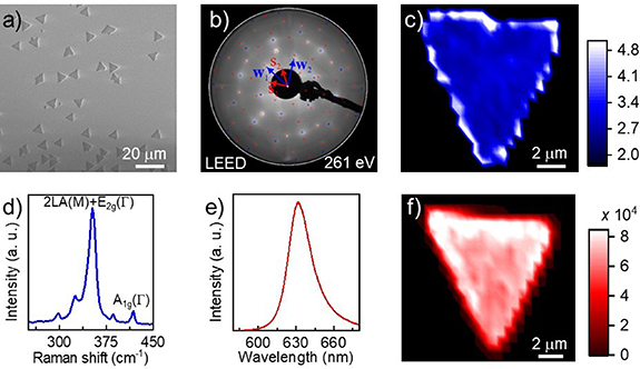
Figure 1. Characterization of WS2 grown on α-Al2O3. (a) SEM image of oriented WS2 single-crystals grown on hydrogen-etched α-Al2O3. (b) LEED pattern of WS2 on α-Al2O3 showing the relative orientation of WS2 R30 (W1 and W2 in blue) and Al2O3 (0001) c-plane (S1 and S2 in red). (c) Map of the ratio of the 2LA + E2g/A1g Raman modes. (d) Representative Raman spectrum of WS2, the 2LA + E2g and A1g peaks used in panel (c) are highlighted. (e) Representative PL spectrum of WS2. (f) PL map of WS2 showing the intense emission form the A-exciton at (630.7 ± 0.1) nm (1.96 eV).
Download figure:
Standard image High-resolution imageRaman mapping (figure 1(c)) and spectroscopy (figure 1(d)) confirm that WS2 is monolayer with a high degree of homogeneity. The benchmarking for WS2 monolayer is that the ratio of the 2LA(M) + E2g(Γ) and A1g(Γ) Raman modes is higher than 2.2, as previously demonstrated in [61]. It is worth noting that the increase of the 2LA(M) + E2g(Γ)/A1g(Γ) ratio on the edge of the crystal, visible in figure 1(c), is an intrinsic artifact of high-resolution Raman mapping. When the laser reaches the edge of the crystal, there is a concurrent decrease of all mode intensities and the intensity of the A1g(Γ) goes close to noise level, causing an increase of the 2LA(M) + E2g(Γ)/A1g(Γ) ratio. PL measurements (figures 1(e) and (f)) also confirm that the synthesized WS2 is monolayer: the room-temperature PL spectrum, reported in figure 1(e), shows an intense emission at (630.7 ± 0.1) nm (1.96 eV), related to the exciton of monolayer WS2. The PL peak is slightly red-shifted if compared to the PL peak position typically observed for WS2 on sapphire (∼620 nm) [57, 62–64]. Moreover, this peak has a strong asymmetry, showing a tail on the high wavelength side. These results are likely due to the presence of intra-gap states related to sulfur vacancies, as reported by Carozo et al [65]. The PL map (figure 1(f)) shows an increase of intensity at the edges of the crystal, while the center shows homogeneous PL signal, as it was also previously reported [13, 66]. The statistic distributions of 2LA(M) + E2g(Γ)/A1g(Γ) ratio, A1g(Γ) Raman shift, PL intensity and PL position are reported in figure S1 (available online at stacks.iop.org/JPMATER/4/024002/mmedia).
3.2. Thermal stability of monolayer WS2
To investigate the stability of WS2 in typical BEOL conditions, freshly grown WS2 single-crystals were initially annealed at a temperature of 300 °C and medium-vacuum (pressure of 10−3 mbar). These conditions were chosen to be as close as possible to those at which 2D materials are usually exposed during device fabrication steps [50, 51], i.e. dielectric deposition, metal evaporation or post-deposition annealing. To further mimic typical device fabrication flows, in which the sample is subjected to multiple heatings during the different processing steps, the annealing (cumulatively 10 h long) was interrupted several times (i.e. after 30 min, 1 h, 3 h and 10 h) and the sample characterized after each step by means of SEM, Raman and PL spectroscopies, which have been suggested as inline metrology for TMD-Si BEOL flow [27] (details in the Experimental section). This intermediate characterization, indeed, is often carried out to monitor the quality of the material and of the assembling device during its fabrication. In figure 2 the characterization of WS2 after sequential annealing steps is reported. From SEM micrographs (figures 2(a)–(c)) a change of shape of the crystal is visible already after 3 h of annealing (i.e. 30' + 30' + 2 h), suggesting that the irregular edges of the as-grown WS2 (figure 2(a)) are more reactive than the center of the single-crystal, in agreement with previous results [47, 67]. After 10 h annealing (i.e. 30' + 30' + 2 h + 7 h) (figure 2(c)) small triangular holes are also visible both on the edges and in inner areas of the crystal (white triangles), indicating loss of WS2 material. Additional SEM micrographs taken on the same sample after the fifth and sixth annealing steps, for a total of 15 and 20 h, are reported in figures S2(a) and (b). Triangular holes, already visible on the edge of the crystal after 10 h annealing, become increasingly larger (i.e. lateral size up to 500 nm) and denser on the entire crystal, with a decrease of the overall area of WS2 monolayer from ∼81 μm2 (as grown) down to ∼74 μm2 (20 h annealing).

Figure 2. Effect of multiple annealings of WS2 at 300 °C and 10−3 mbar. (a)–(c) SEM micrographs of WS2 as grown and after three steps (cumulative 3 h) and four steps (cumulative 10 h) annealing at 300 °C. (d) and (e) Raman and PL spectra, respectively, of WS2 after multiple annealings at 300 °C taken after each step.
Download figure:
Standard image High-resolution imageFigure 2(d) shows the evolution of the Raman spectrum after multiple annealing steps from 30 min up to 10 h, carried out through four sequential steps. The annealing in these conditions mainly affects the intensity of the 2LA(M) + E2g(Γ) Raman mode: as shown in figure 2(d), after a first slight increase (30 min), the 2LA(M) + E2g(Γ) intensity slowly decreases for the subsequent steps. Raman spectra taken after additional annealing steps of 15 and 20 cumulative hours are reported in figure S2(c), in which a large decrease of the 2LA(M) + E2g(Γ) peak intensity is visible, down to a minimum of 52% of the starting value (i.e. after 20 h). The decrease of the intensity of the 2LA(M) + E2g(Γ) mode for annealings longer than 1 h is related to the formation of holes in the WS2 crystal (figures 2(a)–(c)) and therefore to a loss of the overall quantity of material analyzed under the laser spot. The PL spectra for each annealing step are reported in figure 2(e). The PL peak related to the WS2 A-exciton before annealing lies at (630.7 ± 0.1) nm (1.96 eV) with a full width at half maximum (FWHM) of (14 ± 1) nm. Upon annealing, the PL intensity rapidly decreases and becomes negligible after 15 h at 300 °C (figure S2(d)). After the first annealing step, the PL blue shifts down to (623 ± 0.2) nm (1.99 eV), while with increasing annealing time, it red-shifts up to (644.2 ± 0.2) nm (1.93 eV) with a concurrent broadening (FWHM (29 ± 1) nm). The first blue-shift of PL can be attributed to residual contaminations deposited on the growth substrate desorbing during the first annealing step. The subsequent broadening and red shift of the PL peak is likely due to a higher population of point defects such as sulfur vacancies (e.g. at the edge of the triangular holes), a hypothesis that is supported by several works [65, 67, 68]. The PL peak broadening is also combined with an increase of peak asymmetry. This asymmetry is due to the presence of an additional luminescence peak at about 650 nm, which is related to sulfur vacancy bound excitons [65, 66].
From these preliminary results, one might conclude that monolayer WS2 is not stable at 300 °C in medium-vacuum and that its properties rapidly degrade after the first few annealing steps. However, this large instability at relatively low temperature and pressure is in contrast with both the melting and the dissociation temperatures of bulk WS2, which are around 1250 °C [69] and 1040 °C [70], respectively. Also, such degradation is more dramatic than that reported by Rong et al [46], who observed that after 20 min of annealing at 380 °C in air, only highly defective areas of polycrystalline WS2 start to degrade. The fast degradation of monolayer single-crystal WS2 reported in figure 2 might then have been accelerated by external events and can have different origins: (a) the generation of defects upon exposure to laser and/or electron beam during the intermediate characterization analyses; (b) the presence of a relatively high concentration of residual oxide species in the chamber during the annealing at the vacuum level employed; (c) the exposure to air after each annealing step.
To shed light on this, each of the possible degradation causes was systematically studied. First, the role of intermediate characterization after each annealing step was evaluated by analyzing two different areas, namely 1 and 2, of a fresh WS2 sample using SEM, Raman and PL spectroscopies, respectively. In figure 3(a) (area 1) two WS2 crystals (black arrows) were imaged using only SEM with e-beam current 12 pA (specimen current <0.5 pA); otherwise the sample was left in dark. The WS2 crystal reported in figure 3(c) (area 2, white arrow) was additionally characterized using Raman and PL spectroscopies with laser power set to 730 μW (fluence 9.4 mJ μm−2), as in figure 2. The values of both e-beam current for SEM imaging and laser fluence for Raman and PL spectroscopies were chosen to be compatible with typical values used to characterize TMDs on insulating substrate, i.e. sapphire. Higher e-beam current would lead to charging of the sample during SEM analysis, while higher laser fluence can damage the exposed material. The sample was then annealed at 300 °C and 10−3 mbar for 10 h in a continuative manner. While no difference is visible in the morphology of the crystal in area 1 before and after annealing (figures 3(a) and (b)), a large morphological degradation is observed for the WS2 crystal in area 2, which was exposed to a laser power of 730 μW (white arrow, figures 3(c) and (d)). Moreover, both Raman and PL signals of the analyzed crystal in area 2 largely decrease after the continuative annealing at 300 °C (figures 3(e) and (f)). These results suggest that the values of e-beam current typically used for SEM on sapphire preserve the intrinsic stability of WS2 at 300 °C and medium-vacuum (10−3 mbar), even if heated for 10 continuative hours. Conversely, the previous exposure of WS2 single-crystal to a focused laser (∼1 μm) with fluence 9.4 mJ μm−2 appears to trigger the instability of WS2, which then degrades upon annealing.

Figure 3. Analysis of the influence of intermediate characterization on the stability of WS2 at 300 °C. (a) and (b) SEM micrographs of WS2 exposed only to SEM beam before (a) and after (b) annealing at 300 °C. (c) and (d) SEM micrographs of WS2 exposed to both SEM beam and green laser with laser power of 730 μW before (c) and after (d) annealing at 300 °C. (e) and (f) Raman and PL spectra, respectively, before and after annealing of sample shown in panels (c) and (d). (g) and (h) SEM micrographs of WS2 exposed to both SEM beam and green laser with laser power of 73 μW before (g) and after (h) annealing at 300 °C. (i) and (j) Raman and PL spectra, respectively, before and after annealing of sample shown in panels (g) and (h).
Download figure:
Standard image High-resolution imageTo further investigate the relation between laser fluence and thermal instability of WS2, an additional area (area 3) was characterized using Raman and PL spectroscopies with laser power set to 73 μW (fluence 0.9 mJ μm−2) prior the annealing at 300 °C and 10−3 mbar for 10 h (figures 3(g)–(j)). Panels 3(g)–(j) report the SEM micrographs and the Raman and PL spectra of WS2 exposed to laser power of 73 μW (fluence 0.9 mJ μm−2), before and after annealing: no clear difference in the morphology nor in Raman or PL signal is visible. These results indicate that WS2 is intrinsically stable at 300 °C in medium-vacuum as long as the degradation is not triggered by the exposure to laser with a fluence higher than a certain threshold (9.4 mJ μm−2). On the contrary, below this threshold, the thermal stability is preserved.
It is interesting to note that, even when the degradation of WS2 is triggered by exposing the single-crystal to a relatively high-power laser, this phenomenon is localized only to the exposed area, as shown in figure 3(d). After the annealing, the previously exposed crystal (white arrow) is nearly destroyed, while a small WS2 crystal next to it (figure 3(d), up left corner) appears to be fully preserved. These results also rule out that oxidative species in the chamber might be responsible for the degradation observed in figure 2 (hypothesis (b)), as both Raman and PL of WS2 (figures 3(i) and (j)) are unaffected after a 10 h annealing in the chamber. It is also worth mentioning that the different levels of degradation for WS2, exposed to a laser power of 730 μW (fluence 9.4 mJ μm−2) and annealed for 10 h in a multiple (figure 2(c)) and continuative (figure 3(d)) manner, are expected to be related only to the different mapping methods adopted in the two experiments (see figure S3 for further details).
In figure 4, the role of the pressure in the chamber is taken under consideration by annealing WS2 at 10−8 mbar (high-vacuum) for 10 h: again, no large difference after the annealing is observed if the sample is only analyzed by means of SEM with e-beam current set to 12 pA (panels (a) and (b)), as typically used for insulating substrates, and laser fluence of 0.9 mJ μm−2 (panels (c) and (d)). Both Raman and PL spectra, reported in panels (c) and (d) respectively, confirm that using low laser fluence is safe for WS2: both structural and optical properties of WS2 are seemingly preserved after the annealing in high-vacuum. Indeed, although the PL intensity in panel (d) slightly decreases after annealing, the FWHM of the WS2 A-exciton peak before and after the thermal treatment remains ∼12 nm with no redshift, indicating that the optical properties of WS2 are not considerably degraded by the treatment. As the annealing was performed in a chamber adopted for XPS analysis, it was also possible to perform chemical characterization of the as-grown sample and monitor the effect that such a long annealing (i.e. 10 h) has on WS2 chemical composition. The plots in figure 4(e) show the high-resolution spectra, after background subtraction, acquired within the BE window of tungsten W 4f and sulfur S 2p core electrons, before and after the continuative high-vacuum annealing, respectively. In order to study the chemistry of the sample surface, a deconvolution of the experimental curves was performed. The tungsten spectrum of the as-grown sample can be fitted as the superposition of three doublets, with the W 4f7/2 components at (32.1 ± 0.1) eV (yellow), (32.9 ± 0.1) eV (light-blue) and (36.0 ± 0.1) eV (pink), respectively. The W 5p3/2 peaks are shifted 5.8 eV above the corresponding W 4f7/2. Both the yellow and light-blue W 4f doublets at lower BE have their counterpart in the sulfur spectrum, which shows two doublets with S 2p3/2 components at (161.7 ± 0.1) eV and (162.5 ± 0.1) eV. The yellow and light-blue peaks are ascribed to atoms belonging to WS2 crystals, while the pink doublet was ascribed to residuals of unreacted WO3 precursor. In particular, the energy position of the light-blue subcomponent is in perfect agreement with the one reported in literature for the hexagonal WS2 semiconducting phase (2H), while the lower BE of about 0.8 eV related to the yellow minor subcomponent can be a fingerprint of the 1T-WS2 metallic phase, sulfur vacancies or other kinds of defects due to CVD growth process [45, 71, 72]. Interestingly, the spectra acquired after 10 h continuative annealing at 300 °C in high-vacuum show almost unaltered yellow and light-blue components. The only significant change in the W spectrum is related to the WO3 doublet (due to unreacted material on the sapphire surface) [37], which shows a decreased contribution to the W 4f envelope in comparison to the pre-annealing data. Moreover, a new W-related doublet (green) appears at (33.6 ± 0.1) eV, which does not have a counterpart in the S 2p spectrum acquired after the annealing. The green component can be ascribed to a chemical evolution into lower valence oxides of the unreacted WO3 [73] as a consequence of the high-vacuum annealing, which, however, does not have any sizeable effect on the thermal stability of WS2 crystals.
The absence of modifications in the surface chemistry of WS2 crystals, confirmed by XPS results, is also particularly important since desorption of sulfur in a BEOL could cause line contamination.
To investigate whether the exposure of the sample to air after each annealing step (listed as cause (c)) might contribute to the fast degradation reported in figure 2, a fresh sample was annealed at 300 °C in medium-vacuum in two subsequent steps of 10 h each and analyzed using the safe conditions found in figure 3. No clear difference is observed from the SEM, Raman and PL analyses on the same crystal (figure S4), confirming that, if no oxidation is triggered by a relatively high-power laser, WS2 is intrinsically stable at 300 °C and medium-vacuum even when exposing the sample to air in-between multiple annealings.
Finally, the thermal stability of WS2 at high temperatures was also investigated by annealing a fresh sample of WS2 at 600 °C and 10−3 mbar. Figure S5 shows that at this annealing temperature WS2 becomes unstable and completely degrades after 1 h. The XPS spectra of a sample after 2 h annealing under the abovementioned conditions show a complete absence of WS2 related components and that traces of tungsten oxides are the only remaining species (figure S5(e)).
3.3. Compatibility of monolayer WS2 with typical BEOL conditions
The results reported in this work indicate that monolayer single-crystal WS2 is intrinsically stable at 300 °C, a typical temperature adopted in BEOL fabrications steps, even for 10 h. However, care must be taken in order to preserve its thermal stability and the appropriate conditions for handling the sample between each step must be carefully chosen. A schematic summary of the conditions investigated in this work is reported in figure 5. If a base pressure of 10−3 mbar (or lower) is used when annealing at 300 °C, WS2 does not degrade: the vacuum level is low enough to avoid fast oxidation of WS2 at a relatively high temperature.

Figure 4. Analysis of the thermal stability of WS2 at 300 °C in high-vacuum (10−8 mbar). (a) and (b) SEM micrographs of WS2 before (a) and after (b) annealing at 300 °C. (c) and (d) Raman and PL spectra, respectively, before and after annealing of the sample shown in panels (a) and (b). (e) XPS high-resolution W 4f and S 2p experimental spectra (markers) and fitting results (black line) before and after 10 h continuative high-vacuum annealing.
Download figure:
Standard image High-resolution image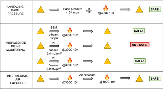
Figure 5. Schematic summary of the thermal stability of WS2 in the conditions studied in this work. At a chamber pressure ⩽10−3 mbar, the vacuum level is high enough to prevent oxidation of WS2 at 300 °C. Intermediate inline monitoring of WS2 using SEM with an e-beam current of 12 pA or PL using fluence ⩽0.9 mJ µm−2 are compatible with annealing WS2 at 300 °C and medium-vacuum. PL with a laser fluence equal to 9.4 mJ µm−2 instead induces defects. Intermediate exposure to air of WS2 in-between annealing steps is compatible with the thermal stability of WS2 at 300 °C and medium-vacuum.
Download figure:
Standard image High-resolution image
The inline monitoring of the sample in-between annealing steps needs to be carefully performed. In fact, monolayer WS2 remains stable at 300 °C and 10−3 mbar as long as the degradation is not triggered by exposure to a focused light with relatively high power, in agreement with previous reports [56, 57]. The exposure to laser above a certain threshold either generates or activates defects, i.e. sulfur vacancies, which then rapidly react at high temperature with oxidative species that are still present in the annealing chamber at a pressure of 10−3 mbar. However, if the laser fluence is lowered down to ⩽0.9 mJ μm−2 (laser power 73 μW), this photo-induced process is not activated. Atkin et al [56] reported a fluence threshold of defect photo-activation for WS2 between 2 and 20 mJ μm−2 at room temperature [56]. They suggest that if the laser exposure is energetic enough the top sulfur layer of WS2 is affected, generating localized defects (i.e. contaminant adsorption), and becomes more susceptible to deterioration; below the threshold, instead, the reaction is not activated. Our experiments indicate that carrying out analysis with a light fluence of 0.9 mJ μm−2 is safe for monolayer WS2, even when annealing at 300 °C and in medium-vacuum. Moreover, multiple exposures to the laser with light fluence of 0.9 mJ μm−2 and different combinations of laser power and exposure time (i.e. laser power 730 μW, exposure time 1 s, fluence 0.9 mJ μm−2) were taken into consideration and no major difference was observed.
On the contrary, SEM analysis with an e-beam current of 12 pA does not induce degradation of WS2 single-crystals. A relation between e-beam current and defect activation of WS2 might be expected, similarly to the laser fluence. In perspective of BEOL integration on a Si platform, particular care should be adopted and the effect of higher electron currents on monolayer WS2 should be investigated.
Finally, the effect of ambient exposure in-between processing steps was investigated by annealing WS2 at 300 °C in two subsequent steps of 10 h each. It was found that WS2 is compatible with sequential fabrication steps at this temperature and in medium-vacuum.
4. Conclusions
In summary, in this work the thermal stability of monolayer single-crystal WS2 at 300 °C in medium- (10−3 mbar) and high- (10−8 mbar) vacuum was investigated. These conditions were chosen to be as representative as possible to typical BEOL conditions, at which WS2 would be exposed if integrated in wafer-scale device fabrication flows. Epitaxial monolayer WS2 grown on sapphire was first annealed in these conditions via four sequential steps for a total time of 10 hours. After each step, the sample was unloaded and fully analyzed by means of SEM, Raman and PL spectroscopies, in a way that can mimic the fabrication & control method typically used in device fabrication procedures. It was found that, if high laser fluence (power 730 μW, fluence 9.4 mJ μm−2) was used for the spectroscopic analyses, WS2 rapidly degraded in these thermal conditions with a large deterioration of its chemical and structural properties, resulting in a large quenching of its optical properties. On the contrary, if a laser fluence of 0.9 mJ μm−2 was used, monolayer WS2 did not degrade upon annealing at 300 °C and medium- or high-vacuum. From these results, it can be concluded that WS2 can undergo processing steps involving a temperature of 300 °C (in a non-reactive atmosphere) in medium- and high-vacuum, provided that the intermediate characterization steps are carried out compatibly with the photo-activation threshold of WS2 oxidation. This compatibility can be achieved by either working with a laser fluence below the threshold or by choosing a sacrificial crystal on which the characterization is carried out.
Acknowledgments
The research leading to these results has received funding from the European Union's Horizon 2020 research and innovation program under Grant Agreement Nos. 785219-GrapheneCore2 and 881603-GrapheneCore3 and from Compagnia di San Paolo (project STRATOS).