

Abstract
The development of systems for the deterministic transfer of two-dimensional (2D) materials have undoubtedly contributed to great advancements in 2D materials research. In fact, they have made it possible to fabricate van der Waals heterostructures and 2D materials-based devices with complex architectures. Nonetheless, as far as we know, the number of existing papers providing enough details to reproduce these systems by other research groups is very scarce in the literature. Moreover, these systems typically require the use of expensive optical and mechanical components hampering their applicability in research groups with a low budget. Here, we demonstrate how a deterministic placement system for 2D materials, set up with full capabilities, can be implemented for under 900 € -- which can be easily implemented in labs and educational labs with low budgets.
Export citation and abstract BibTeX RIS

Original content from this work may be used under the terms of the Creative Commons Attribution 4.0 licence. Any further distribution of this work must maintain attribution to the author(s) and the title of the work, journal citation and DOI.
After the isolation of graphene and other two-dimensional (2D) materials in 2004–2005 [1, 2], the development of the transfer methods to deterministically place 2D materials at specific locations with high accuracy is one of the most importants breakthrough in 2D materials research [3–8]. In fact, these deterministic transfer methods have made possible, the fabrication of artificial materials by the stacking of dissimilar 2D materials on top of each other in what is called nowadays van der Waals heterostructures [9–15].
The implementation of experimental setups for the deterministic placement of 2D materials, however, typically requires costly optical and mechanical components, hampering their implementation in labs with modest budget and their use in science education and public demonstrations. Although, previously, some of the authors of this work reported all the details to build up a transfer setup with an approximate cost of 7000–8000 € (much cheaper than commercially available systems or conventional transfer setups based on retrofitted metallurgical microscopes or probe stations) [8] this cost can be still a big handicap for the applicability of the system. Here, we report all the details to install a fully functional deterministic transfer setup at a total cost under 900 € and with a very compact footprint. The performance of this system is illustrated by placing a few-layer thin InSe flake bridging two electrodes.
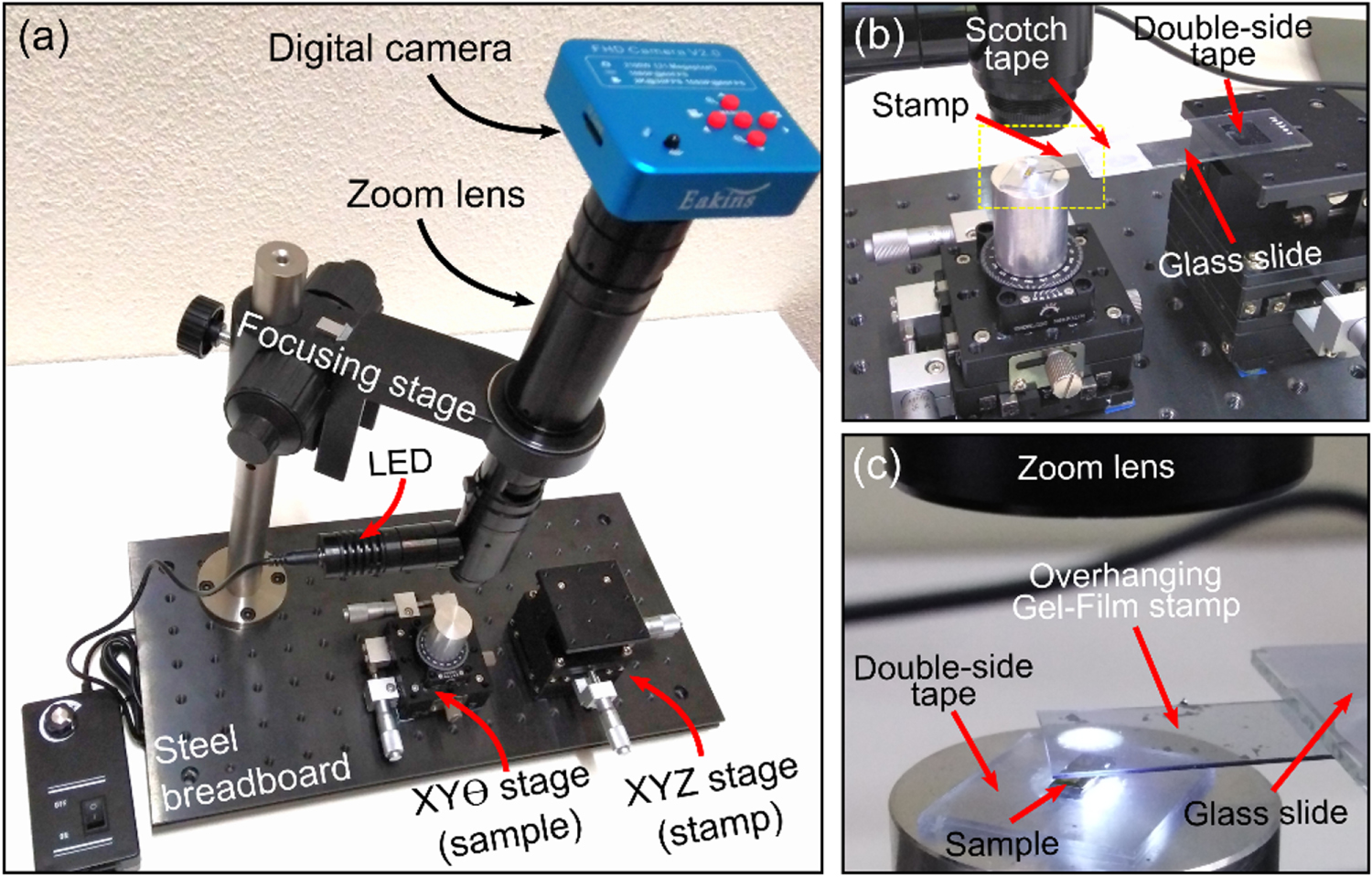
Figure 1(a) shows a picture of the presented system to transfer 2D materials. The system is basically composed of a zoom lens with coaxial illumination, a XY + rotation manual stage (sample/substrate stage) and a XYZ manual stage (stamp stage). The zoom lens is supplemented with a 21-megapixel digital camera with HDMI output and all the components are mounted on a magnetic breadboard. The manual stages are attached to the breadboard through magnets glued at the base of the stages. Figure 1(b) shows a close-up picture of the sample and stamp stages where it is shown how the stamp is mounted. We employ a rectangular piece (5 mm by 10 mm approx.) of Gel-Film (WF x4 6.0 mil, by Gel-Pak®) as viscoelastic stamp. Unlike in our previous work, in which we used the PF Gel-Film, we now use the WF Gel-Film that has the polydimethylsiloxane (PDMS) -based gel material bonded to a flexible and quasi transparent backing polyester substrate. The Gel-Film stamp is glued to a glass slide with Scotch tape, leaving most of the stamp overhanging (protruding from the glass slide as shown in figure 2(c)). We have found that this 'cantilever-like' geometry of the stamp is more advantageous for the deterministic placement of 2D materials than the stamp geometry used in our early work in [8]. Then double-side tape (Scotch® Restickable Tabs) is used to fix the glass slide to the stamp stage and the sample to the sample stage.

Figure 1. (a) Picture of the assembled low-cost system to transfer 2D materials, highlighting some of the key components and details used for deterministic transfer process. (b) Zoomed in picture showing details of the stamp clamping and fixture to the XYZ stage. (c) Zoomed in image of the area highlighted with a dashed yellow rectangle in (b) where the sample and stamp fixture are displayed.
Download figure:
Standard image High-resolution image
Figure 2. Schematics and transfer process of bridging a thin InSe flake onto the pre-patterned gold electrodes on a 285 nm SiO2/Si substrate, including empty pre-patterned gold electrodes (1), isolated thin InSe flake on the surface of the Gel-Film stamp (2), alignment of the flake with the electrodes (3), the stamp is gently pressed against the target sample (4), the stamp is slowly peeled off (5, 6, 7, white arrows indicate the stamp/air interface) and final device (8).
Download figure:
Standard image High-resolution imageTable 1 summarizes all the different parts needed to implement the system and the reader will find a thorough step-by-step guide to assemble it in the supporting information is available online at stacks.iop.org/JPMATER/3/016001/mmedia. A list of consumables required to use the deterministic transfer system is shown in table 2.
Table 1. Summary of the components of the proposed system. (Note: hyperlinks for the different items are available in the online version of the manuscript).
| Description | Distributor | Price (€) | ||
|---|---|---|---|---|
| System base | Ferromagnetic steel optical breadboard | Standa | 1BS-2040-015 | 130.00 |
| Rubber damping feets (set of 4) | Thorlabs | RDF1 | 4.92 | |
| Imaging system | Ø25.0 mm pillar post | Thorlabs | RS300/M | 53.25 |
| Mounting post base | Thorlabs | PB1 | 22.44 | |
| Focusing stage for zoom lens | Aliexpress | 56.96 | ||
| 400× zoom lens with coaxial illuminator | Aliexpress | 174.83 | ||
| Auxiliary 3.5× magnification lens | Aliexpress | 34.36 | ||
| 21 MPix digital camera | Aliexpress | 74.70 | ||
| 22'' HDMI monitor | Amazon | 89.99 | ||
| Sample and stamp stages | Manual rotation stage (for sample) | Thorlabs | MSRP01/M | 66.53 |
| XY manual stage (for sample) | Banggood | 63.14 | ||
| XYZ manual stage (for stamp) | Banggood | 81.18 | ||
| Magnets (for sample and stamp stages) | Amazon | 7.15 | ||
| Total: | 859.45 | |||
Table 2. Summary of the consumables (optional ones marked with *). (Note: hyperlinks for the different items are available in the online version of the manuscript).
| Description | Distributor | Price (€) | |
|---|---|---|---|
| Gel-Film sheet (viscoelastic stamp) | Gel-Pak | WF-30-x4-6mil | 5.00 |
| Nitto tape (for exfoliation of layered crystals) | Amazon | SPV224 | 15.00 |
| Scotch restickable tabs (to attach sample and stamp to their stages) | Amazon | 5.11 | |
| Cyanocrylate based glue | Amazon | 4.35 | |
| Pre-patterned electrodes (20×) * | Ossila | S403A2 | 60.00 |
| Natural bulk 2D crystals (graphite, MoS2, mica...) * | Mineral shop | 1–100 each | |
| Artificial bulk 2D crystals * | HQ Graphene, 2D Semiconductors, 2D-material | 200–600 each | |
In order to illustrate the potential of this inexpensive transfer setup, figure 2 shows how one can use this deterministic transfer setup to fabricate a 2D material based field effect transistor. The process starts by exfoliating a bulk crystal of a layered material (in this case a synthetic bulk crystal of InSe, an n-type semiconductor) with Nitto SPV224 tape. The crystals adhered to the surface of the tape are then transferred to the surface of the Gel-Film stamp by gently pressing the tape against the Gel-Film surface and suddenly peeling off the tape. Then, the surface of the Gel-Film stamp is inspected under an optical microscope to find the flake that the operator wants to transfer. Note that the stamp can be inspected under the zoom lens imaging system of the transfer setup to identify the flakes if a metallurgical microscope is not available. See the supplementary material for a comparison between the image quality obtained with the zoom lens system of the transfer setup and with a metallurgical microscope.
As a target substrate we use a SiO2/Si substrate (285 nm of SiO2) with pre-patterned electrodes (Ossila®) separated by 30 μm (step 1). The InSe flake that we want to transfer can be found under the inspection of the zoom lens imaging system by focusing on the surface of the stamp (step 2). The stamp is brought closer to the surface of the sample and the flake is aligned with the electrodes employing the XYZ stamp stage micro-positioner (step 3). The stamp is gently lowered until it contacts the surface of the sample (step 4). Then the stamp is slowly peeled off (steps 5 to 7) until it is completely removed and the InSe has been successfully transferred bridging the two electrodes (step 8). The peeling off process takes place by lifting up the Z-micromanipulator of the stamp stage at an approximate speed of 0.25–0.50 mm min−1. Note that these values are a rough indication as the precise lifting speed is usually adjusted by inspecting the peeling off process with the imaging system during the lifting.
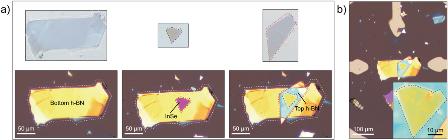
Another widespread use of systems for the deterministic placement of 2D materials is the fabrication of van der Waals heterostructures. In figure 3 we demonstrate that our inexpensive deterministic transfer system can be also used to fabricate van der Waals heterostructures by fabricating a fully encapsulated InSe flake between two hexagonal boron nitride (h-BN) flakes. Figure 3(a) shows the sequence of transfer. First, a h-BN flake is transferred in the middle of a pre-pattern cross-hair marker structure (left column). Second, a InSe flake is transferred onto the bottom h-BN flake (middle column). Finally, another h-BN flake is transferred sandwiching the InSe flake between h-BN sheets (right column in figure 3(a)). Figure 3(b) shows the resulting van der Waals heterostructure.

Figure 3. Fabrication process of a fully encapsulated InSe flake heterostructure with h-BN onto a pre-defined location on a SiO2/Si substrate. (a) Sequence of stacking bottom h-BN (left), thin InSe (middle) and top h-BN (right) by the deterministic transfer method. (b) The overall resulting h-BN/InSe/h-BN heterostructure in the middle of a pre-patterned cross-hair and a zoom-in image of the fully encapsulated InSe flake (inset panel).
Download figure:
Standard image High-resolution imageFinally, we demonstrate how one can use this inexpensive transfer setup to fabricate not only simple devices nor isolated van der Waals heterostructures but also fully-encapsulated electronic devices. Hexagonal boron nitride (h-BN) is an atomically flat insulator with a very low density of Coulomb scattering centers and thus by sandwiching a 2D material between two layers of h-BN provides a very clean dielectric environment preserving the intrinsic electronic properties of the encapsulated material. Because of this, the best performances have been reported for electronic devices based on 2D materials encapsulated between h-BN layers [16, 17]. figure 4 shows the steps needed for the assembly of a fully encapsulated InSe device using our transfer setup. A bottom narrow h-BN flake is transferred bridging two pre-patterned gold contacts, then a long InSe flake is transferred on top of the h-BN flake protruding and contacting the two gold contacts. Finally, a large h-BN flake is transferred on top. The result is a gold contacted InSe device, fully encapsulated between h-BN flakes.

Figure 4. Fabrication steps of a InSe device fully encapsulated between h-BN flakes. Pre-patterned gold electrodes on SiO2/Si substrate (1), bottom h-BN flake is transferred (2), InSe flake is transferred bridging the two gold electrodes (3) and transfer of a top h-BN to complete the full encapsulation.
Download figure:
Standard image High-resolution image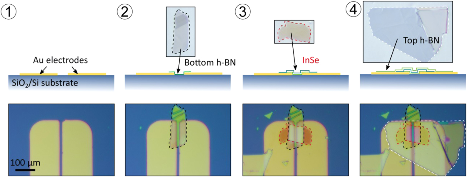
Conclusions
In summary, we presented an inexpensive system to transfer 2D materials that can be easily implemented in labs and educational labs with low budgets, which can also be used for public demonstrations. Moreover, we believe that this transfer system can also help to reduce the entry threshold to work in the field of van der Waals heterostructures. The whole system can be assembled for less than 900 € and the final system has a very compact footprint (making it easy to transport for educators and public demonstrations). We demonstrate that despite the low cost of the system, it has a functionality comparable to that of more expensive setups. In fact, we show how the system can be used to fabricate devices based on 2D materials and could even allow a motivated physics teacher to build basic, yet functional devices like transistors or solar cells out of two-dimensional crystals, together with their class.
Acknowledgments
We would like to thank the input received from the Reviewers that have improved substantially this manuscript. This project has received funding from the European Research Council (ERC) under the European Union's Horizon 2020 research and innovation programme (Grant Agreement No. 755655, ERC-StG 2017 project 2D-TOPSENSE). R F acknowledges support from the Spanish Ministry of Economy, Industry and Competitiveness through a Juan de la Cierva-formación fellowship 2017 FJCI-2017-32919. Q H Z acknowledges the grant from China Scholarship Council (CSC) under No. 201700290035.