

Abstract
High-performance perovskite light-emitting diodes (PeLEDs) require a high quality perovskite emitter and appropriate charge transport layers to facilitate charge injection and transport within the device. Solution-processed n-type metal oxides represent a judicious choice for the electron transport layer (ETL); however, they do not always present surface properties and energetics compatible with the perovskite emitter. Moreover, the emitter itself exhibits poor nanomorphology and defect traps that compromise the device performance. Here, we modulate the surface properties and interface energetics between the tin oxide (SnO2) ETL with the perovskite emitter by using an amino functionalized difluoro{2-[1-(3,5-dimethyl-2H-pyrrol-2-ylidene-N)ethyl]-3,5-dimethyl-1H-pyrrolato-N}boron compound and passivate the defects present in the perovskite matrix with carbon-polymer core–shell quantum dots inserted into the perovskite precursor. Both these approaches synergistically improve the perovskite layer nanomorphology and enhance the radiative recombination. These properties resulted in the fabrication of near-infrared PeLEDs based on formamidinium lead iodide (FAPbI3) with a high radiance of 92 W sr−1 m−2, an external quantum efficiency (EQE) of 14%, reduced efficiency roll-off and prolonged lifetime. In particular, the modified device retained 80% of the initial EQE (T80) for 33 h compared to 6 h of the reference cell.
Export citation and abstract BibTeX RIS

Original content from this work may be used under the terms of the Creative Commons Attribution 4.0 license. Any further distribution of this work must maintain attribution to the author(s) and the title of the work, journal citation and DOI.
1. Introduction
Metal halide perovskite emitters offer significant advantages such as easy tuning of their bandgap through compositional engineering and size tuning in the case of nanocrystals, photoluminescence (PL) quantum yields close to unity across a broad range of emission colors and symmetrical narrow emission spectra [1–4]. Thanks to these properties, it is anticipated that they can be suitable candidates for light emitting diodes with tunable color emission ranging from ultra-violet to the near-infrared (NIR) region [5–7]. Despite the remarkable progress shown by light-emitting diodes based on perovskites (PeLEDs) with external quantum efficiencies (EQEs) recently exceeding 23% [8, 9], significant challenges remain unsolved, including inability to access long wavelength (>1000 nm) emission, significant efficiency roll-off and short lifetime [10–12]. Optimizing the properties of the perovskite layer and the interfaces is of vital importance in order to achieve efficient and stable devices.
Modulation of the perovskite nanomorphology is imperative in order to enhance the performance of these devices. For example, three-dimensional perovskite emitters exhibit fast electron–hole dissociation, which decreases the probability of radiative recombination events. Strategies pursuing the confinement of charge carriers through reduction in the grain size can alleviate this issue [13–16]. In addition, the incorporation of passivation agents into the precursor solution can also modify the resultant perovskite film morphology, while also passivate defects that act as non-radiative recombination centers [17, 18]. Effective passivation materials such as amino-acid additives can coordinate to undercoordinated Pb2+ or halide ions or form ionic bonding to neutralize charged defects [19]; thus improving the device performance [20]. Additionally, carbon quantum dots with different functional groups have been used to passivate the perovskite methyl ammonium lead iodide (CH3NH3PbI3) surface for application in photovoltaics [21]. Dependent on the ligand, this passivation approach either modified the crystal size or decreased the defect density in the perovskite film, thereby promoting efficiency enhancement.
Solution-processed inorganic metal oxides, such as aluminum-doped zinc oxide and SnO2 are common electron transport layers (ETLs) for efficient PeLEDs [22–24]. These materials exhibit adequated n-type conductivity combined with wide bandgaps, thus affording a high transparency within the visible spectrum, a suitable conduction band minimum to match with that of the perovskite emitter and a deep valence band (VB) maximum to afford efficient hole blocking [25]. However, a common issue is their poor interface quality with the perovskite, which can be dentrimental to the device performance [26]. This issue can be overcome with appropriate surface treatment or interface modification [26–28].
Here, we optimize the structural, morphological and optoelectronic properties of a FAPbI3 perovskite emitter through adopting a core-shell carbon-polymer quantum dot (PCD) additive engineering approach. We also modify the surface properties of SnO2 ETL by coverage with an amino-functionalized difluoro{2-[1-(3,5-dimethyl-2H-pyrrol-2-ylidene-N)ethyl]-3,5-dimethyl-1H-pyrrolato-N}boron (BDP). The additive engineering changes the perovskite microstructure and film nanomorphology and reduces non-radiative recombination. The BDP surface modifier on the ETL reduces the electron injection barrier and modulates the surface energy hence altering the perovskite microstructure and film nanomorphology. This synergistic approach enabled the fabrication of NIR PeLEDs (peak emission at 780 nm) with a high radiance of 92 W sr−1 m−2 and EQE of 14%, representing a large improvement compared to the reference device (2.5 W sr−1 m−2 and 6%). These devices also exhibited reduced efficiency roll-off and prolonged T80 lifetime compared to the reference ones.
2. Experimental section
2.1. Perovskite precursor preparation
A 27.7 mg formamidinium iodide (FAI) purchased from GreatCell Solar, 33.2 mg lead iodide (PbI2) obtained from Sigma-Aldrich, and 7.7 mg 5-aminovaleric acid (AVA) purchased from Sigma-Aldrich dissolved in 1 ml of anhydrous N,N-dimethylformamide (Sigma-Aldrich). The precursor solution was stirred for 2 h at 80 °C in an argon-filled glove box before use.
2.2. PeLED fabrication and characterization
Patterned indium-tin oxide (ITO) coated glass substrates with sheet resistance 8 Ω square−1 (Ossila) were used for PeLEDs fabrication. The substrates were cleaned in deionized (DI) water, acetone, and 2-propanol, for 10 min and dried with N2 before they further treated by UV-ozone for 20 min. A solution of colloidal dispersion of tin(IV) oxide in DI water (15%, Alfa Aesar) was spin-coated on ITO substrates at 3000 rpm for 30 s. The SnO2 films annealed at 150 °C for 30 min. For the BDP modified SnO2 films, a solution of 0.5 mg ml−1 in chlorobenzene (CB) was spin-coated at 2000 rpm for 40 s atop SnO2 film. The perovskite precursor solution was spin-coated at 3000 rpm for 1 min, followed by annealing at 100 °C for 16 min. As the hole transport layer (HTL), poly-TPD (poly(N,N'-bis(4-butylphenyl)-N,N'-bisphenylbenzidine), Sigma-Aldrich) was spin-coated from CB solution (13 mg ml−1). Molybdenum oxide (MoO3, 10 nm) and aluminum (Al) were thermally evaporated to serve as the hole injection layer and anode electrode, respectively. For the device characterization, the current density–voltage–luminance (J–V–L) curves, radiance, and EQE were all carried out with an Oriel spectrometer coupled with a fiber integration sphere (FOIS-1) and a Keithley 2400 source meter.
2.3. Characterization methods
Fourier-transform infrared (FT-IR) spectroscopy was performed using a Bruker Tensor 27 spectrophotometer with a DTGS detector. 1H NMR spectra were recorded on a Bruker Avance 500 MHz spectrometer as solutions in deuterated DMSO-d6 using the residual solvent signal as the internal standard and were processed with Topspin 4.0.8. X-ray photoelectron spectrum (XPS) was recorded by a Leybold EA-11 electron analyzer operating in constant energy mode at a pass energy of 100 eV. The x-ray source was a nonmonochromatized Al K line at 1486.6 eV (12 keV with 20 mA anode current). The work function (WF) of pristine and BDP-modified SnO2 films were estimated after recording the ultraviolent photoemission spectra (UPS) of the films deposited on ITO substrates used for PeLEDs fabrication. For the UPS measurements, the He I (21.22 eV) excitation line was used and a negative bias of 12.28 V was applied to the sample in order to separate sample and analyzer high binding energy (BE) cut-offs and estimate the absolute work function value. Atomic force microscopy (AFM) images were captured using an XE7 microscope (Park Systems) by operating in tapping mode. The crystallinity of perovskite films was investigated using an x-ray Siemens D-500 606 diffractometer. UV–Vis absorption spectra of the polymer solutions (concentration 10−5 M) and the prepared films were recorded with a Shimadzu UV-1900 spectrometer. Steady-state PL measurements were performed with a commercial platform (ARKEO—Cicci Research): the substrate was illuminated with a diode-pumped solid-state Nd:YVO4 + KTP laser (peak wavelength 532 nm ± 1 nm, optical power 1 mW on a circular spot of 2 mm of diameter: 31 mW cm−2) at an inclination of 45°. The fluorescence on the opposite side of the substrate is focused on a bundle of fibers (10 mm in diameter) with an aspheric lens close to the substrate to maximize the PL. The bundle sends the signal to a CCD-based spectrometer. Integration time and the number of averaging was maintained the same to better compare the results. Time-resolved PL (TRPL) spectra were measured with an FS5 spectrofluorometer from Edinburgh Instruments. A 478.4 nm laser was used as an excitation source. Scanning electron microscopy (SEM) images of the perovskite films were recorded with a JEOL 7401f FESEM.
3. Results and discussion
3.1. Preparation of core–shell carbon-polymer quantum dots (PCD)
The quantum dots (QDs) used in this study were synthesized through a bottom-up hydrothermal method, according to Ladomenou et al [29]. In brief, citric acid (CA) and ethylene diamine (EDA) were used as starting materials and were reacted in an autoclave, followed by heating at 180 °C for 8 h (figure 1(a)). A purification step took place for the final isolation of the desired product. This method has been previously reported to yield pure carbon quantum dots when heating above 200 °C [30, 31]; however, we intentionally applied here lower temperature during the synthesis in order to receive intermediate products with different degrees of polymerization [32]. We aimed to isolate shell-core polymer-carbon QDs having the molecule 5-oxo-1,2,3,5-tetrahydroimidazo[1,2-α]pyridine-7-carboxylic acid (IPCA) as the polymeric shell. The mixture or assembly IPCA-carbon dots (PCDs) was purified in a 1000 Da dialysis membrane and the fluorophore IPCA has not been removed, as shown in 1HNMR spectra (figures 1(b) and S1). Figure 1(b) (red line) presents a spectrum of QDs that lacks starting materials. The aliphatic protons of carbon cores at 4.2–2.5 ppm are overlapped with two characteristic aliphatic triplet peaks. Then, two peaks at 6.0–5.6 ppm characteristic of double bond confirm the presence of IPCA in the carbon dots solution. Many differences between PCDs and simple carbon dots produced from CA were observed (figure S2).

Figure 1. (a) Synthetic procedure for the preparation of core–shell carbon-polymer (PCD) quantum dots. (b) 1H NMR spectra of CA, EDA and PCD and (c) high resolution TEM image of the synthesized quantum dots. Only the carbon core is clearly seen in this picture.
Download figure:
Standard image High-resolution imageThe existence of carbon core in the PCDs is evident by the transmission electron microscopy (TEM) measurements, presented in figure 1(c). We can conclude that the product contains a carbon core with a diameter of around 2.5 nm. The existence of an extensive amine network in the polymeric shell of these dots is expected to offer bulk and surface passivation in the perovskite through effective coordination with undercoordinated lead cations (Pb2+), which will benefit the device performance and stability.
3.2. Surface modification of SnO2 using amino BODIPY
Besides the emissive layer, the charge injection/transport and interlayer materials also play a crucial role in the device performance, as they dictate efficient charge injection and transport within the device layers and heterointerfaces; they can also modify the nanomorphology of the perovskite emitter deposited atop. Therefore, we first investigated the optoelectronic and structural properties of SnO2 as-deposited and coated with a very thin BDP interlayer (from a 0.5 mg ml−1 solution in CB).
The formation of a thin BDP interlayer on top of SnO2 is evidenced by the XPS measurements, which showed the existence of nitrogen (N) in the BDP covered oxide (termed as the SnO2/BDP sample). Figure 2(a) shows the N1s core level peaks of the XPS spectra taken in pristine SnO2 and BDP/SnO2 [33]. We observe that this BDP has covered the surface of SnO2 having as a result a surface work function (WF) reduction. From the shift towards higher BE in the electron cut-off of the ultra-violet photoelectron spectroscopy (UPS) measurements of BDP/SnO2 (figure 2(b)), a WF reduction of 150 meV (from 4.15 eV to 4.0 eV) is concluded. This shift is due to the formation of a negative interfacial dipole arising from the amino groups, which push electrons toward the SnO2 and effectively reduce its surface WF [34, 35]. This is expected to improve electron injection towards the conduction band of the perovskite emitter [36].
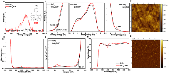
Figure 2. (a) N 1s core level peaks of a SnO2 and SnO2/BDP layers. The chemical structure of amino BDP is shown as inset. (b) UPS spectra of SnO2 and SnO2/BDP films: the high binding energy cut-off (left), the UPS spectra (middle) and the near Fermi level region (right) of the UPS spectra of the prepared samples. (c) UV–Vis absorption spectra, (d) the Tauc plots derived from absorption measurements and (e) transmittance spectra of SnO2 and SnO2/BDP layers on glass/ITO substrates. 10 × 10 μm2 AFM surface topographic images of (f) SnO2 and (g) SnO2/BDP films.
Download figure:
Standard image High-resolution imageOn the other hand, a characteristic peak appears near the onset of the VB, in particular, at around 2.8 eV, in the UPS spectrum of BDP/SnO2. This peak can be attributed to BDP as evidenced by the UPS spectrum of a pristine BDP layer coated (from a 5 mg ml−1 solution in CB) on ITO/glass (figure S3). Figures 2(c)–(e) show the UV–Vis absorption, the derived Tauc plots and transmittance spectra of SnO2 as-deposited and coated with BDP. Whereas the presence of BDP is evident by the characteristics absorption peak at around 500 nm (figure S4), it does not alter significantly the transmittance spectrum of the transparent bottom electrode. In addition, the energy bandgap value (Eg) was calculated from the Tauc plots to be 3.6 eV in both cases.
The surface topography of SnO2 before and after the BDP coverage was further investigated with AFM measurements. Figures 2(f) and (g) show the surface topographies of as-deposited and BDP-modified SnO2, respectively, where it is seen that the BDP modifier has covered the surface of SnO2. The root-mean-square (RMS) surface roughness slightly increased from 0.35 to 1.14 nm, which is not expected to significantly alter the perovskite overlayer. Interestingly, the BDP-modified SnO2 exhibited significant differences in water contact angle (figure 3(a)) and adhesion in DMSO solvent (figure 3(b)), with respect to the pristine SnO2 substrate. In particular, the pristine oxide surface exhibits high hydrophilicity due to the high amount of hydroxyl groups present on the oxide's surface. This, however, has been proven detrimental for the device operation as these negative hydroxyl groups may attract positively charged ions within the perovskite layer [37]. A layer of such positive ions may thus built-up at the respective interface hence upward shifting the vacuum level and increasing the electron injection barrier.
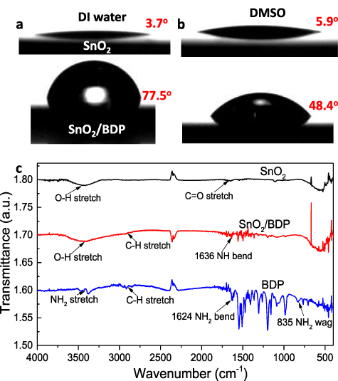
Figure 3. Contact angle measurements taken on a pristine SnO2 (top) and SnO2/BDP substrate (bottom) for a droplet of (a) water and (b) DMSO. (c) FT-IR spectra of pristine SnO2 and BDP films and of a SnO2/BDP layer.
Download figure:
Standard image High-resolution imageFourier-transform infrared measurements were performed for the SnO2 thin film, BDP thin film and BDP coated on top of SnO2 (figure 3(c)). In the FT-IR spectrum of BDP, the bending modes of N–H can be detected at 1624 cm−1 whereas the stretching modes appear at around 3500 cm−1. The characteristic stretching band of SnO2 made by the vibrations of the Sn–O–Sn bond is centered at 640 cm−1. However, tin oxide exhibits a strong broad peak in the 3630–3220 cm−1 area; this is the characteristic stretching band of hydroxyl group (O–H stretching). This band also appears centered around 3430 cm−1 in the SnO2/BDP spectrum but with lower intensity. One possible explanation of this is that in the pure SnO2 film, the surface is rich with hydroxyl groups and with the addition of BDP these groups form extensive hydrogen bond networks with the –NH2 groups of BDP thus being inactivated. As a result, reduced hydrophilicity is obtained for the BDP modified oxide surface, which increases the surface tension and also the measured contact angle for a DMSO droplet. We expect that this will directly influence the nanomorphology of the perovskite overlayer.
To gain an insight into the effect of the SnO2 surface modification on the structural properties and crystallinity of the perovskite film coated atop, x-ray diffraction (XRD) measurements were performed. Figures 4(a) and (b) presents the XRD patterns of FAPbI3 films (without AVA) spin-coated on SnO2 without and with BDP surface modification, respectively. It becomes evident that the characteristic perovskite peaks are more pronounced in the SnO2/BDP/FAPbI3 sample. More interestingly, the full-width-half-maximum of the crystallization peak at ∼13.9° corresponding to the (001) plane is reduced indicating improved film quality with low roughness and smaller overall crystal size of 48.78 nm compared with the 56.57 nm for the FAPbI3 spin-coated on the pristine SnO2. Furthermore, the increased intensity of the same (001) crystallization peak also suggests that the surface modifier of SnO2 enhances the preferred orientation of the perovskite film deposited on top and suppresses the formation of PbI2.

Figure 4. XRD patterns of FAPbI3 films deposited on (a) SnO2 and (b) SnO2/BDP layers. 10 × 10 μm2 AFM surface topography of FAPbI3 perovskite deposited on (c) pristine and (d) surface modified with BDP SnO2 electron transport layer. (e) Steady-state photoluminescence (PL) spectra and (f) transient PL (TRPL) decay curves of FAPbI3 perovskite deposited on pristine and BDP modified SnO2 layer.
Download figure:
Standard image High-resolution imageThe nanomorphology of FAPbI3 perovskite was also altered when coated onto the BDP modified SnO2. AFM 10 × 10 μm2 topographies of a 50 nm thick FAPbI3 deposited on pristine and BDP-modified SnO2 on glass/ITO substrates are shown in figures 4(c) and (d), respectively. In the reference sample, interconnecting grains are observed, which form a 'network' of long perovskite islands. However, in the case of perovskite deposited directly onto BDP, these grains are smaller and separated one from the other. The same conclusion can be drawn from SEM topographic images of the same samples (figure S5). This can be explained by taking into account the reduced hydrophilicity of the BDP-coated SnO2 sample. In hydrophilic surfaces water molecules adsorbed onto them act as nucleation sites for the perovskite formation. As a result, extended perovskite grains are formed in hydrophilic surfaces which are highly desired for perovskite solar cells [37]. However, the situation is different for PeLEDs where smaller grains are necessary in order to confine both charges and excitons and increase the radiative recombination rate [38]. We therefore argue that the decrease in grain size in the perovskite coated onto the BDP modified substrate could be beneficial for LED operation [39]. Additionally, a reduction in surface roughness of the perovskite film deposited onto the BDP-modified ETL (from 22.48 nm for the reference sample SnO2/FAPbI3 to the 19.51 nm for the FAPbI3 deposited on SnO2/BDP) is indicative of a better contact quality between the perovskite emitter and the HTL deposited on top of it.
Moreover, the interfacial electron transport between the perovskite and SnO2 in the absence and presence of the BDP surface modifier was studied by using steady-state PL and transient PL (TRPL) measurements. As shown in figure 4(e), the FAPbI3 coated on the ITO/SnO2/BDP substrate exhibits a 44% reduction in the PL intensity, indicating a faster electron extraction from the perovskite to the metal oxide, which can be due to a reduction in the electron injection/extraction barrier at the interface. This indicates that enhanced electron injection can also be obtained upon the application of a forward bias during the device operation. The same conclusion can be drawn from the decrease in carrier lifetime shown in transient PL (TRPL) spectra of figure 4(f). A red shift of about 10 nm the PL peak is also observed for the BDP/FAPbI3 sample, which can be attributed to changes in the lattice parameters; in particular, a small shift from 13.89° to 13.83° for the (001) XRD peak of BDP/FAPbI3 is also observed. These changes may originate from coordination of the amino groups of the BDP underlayer with undercoordinated I− or Pb2+ within the perovskite lattice resulting in trap filling and better interface quality. Notably, the absorption spectra of the two samples were nearly similar (figure S6).
3.3. Core–shell carbon polymer dots as perovskite additives
To passivate defects present in the perovskite bulk, we next applied PCD as the passivation agent embedded into the FAPbI3 perovskite emitter. We first tested their effect in the perovskite microstructure (without AVA) and the nanomorphology of the resultant perovskite layer (without AVA). Figures 5(a) and (b) shows the SEM images of the perovskite derived from the spin coating (onto glass/ITO substrates) of the precursor solution without and with PCDs (in a concentration of 1 mg ml−1 in the precursor). It becomes evident that PCDs largely affect the layer morphology resulting in the formation of well-defined nanograins of smaller size compared to the reference sample which consists of longer perovskite 'islands'. These small grains can strongly confine excitons and charges therein thus increasing the radiative recombination, which is crucial for perovskites that generally exhibit low exciton BEs of few meV [40]. These grains are slightly decreased in size when coated on top of the BDP layer. Figures 6(a)–(d) depicts the AFM topographies of FAPbI3 films embedding PCD additive in a concentration of 0.4 mg ml−1 and 1 mg ml−1 (named hereafter as FAPbI3 + PCD-0.4 and FAPbI3 + PCD-1, respectively) on top of pristine SnO2 (figures 6(a) and (b), respectively) and on BDP-modified SnO2 substrate (figures 6(c) and (d), respectively). It becomes evident that both layers, FAPbI3 + PCD-0.4 and FAPbI3 + PCD-1, consist of smaller grains when deposited on the BDP modified SnO2 exactly as in the case of pristine perovskite coated on as-deposited and BDP-modified oxides. Additionally, the FAPbI3 + PCD layers deposited on the SnO2/BDP exhibited lower RMS surface roughness compared with the perovskite film coated on the pristine SnO2. Especially, in the case of the FAPbI3 + PCD with concentration of 1 mg ml−1, the RMS was 14.5 nm, while the SnO2/FAPbI3 + PCD-1 exhibited higher RMS of 23.3 nm. This significant improvement in the microstructure of the perovskite embedding PCD and of the nanomorphology of the perovskite film deposited on BDP coated SnO2 is expected to be beneficial for the device performance.
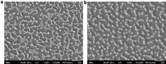
Figure 5. SEM images of a layer derived from (a) a pristine FAPbI3 precursor (without AVA) and (b) the same precursor with PCD additive.
Download figure:
Standard image High-resolution image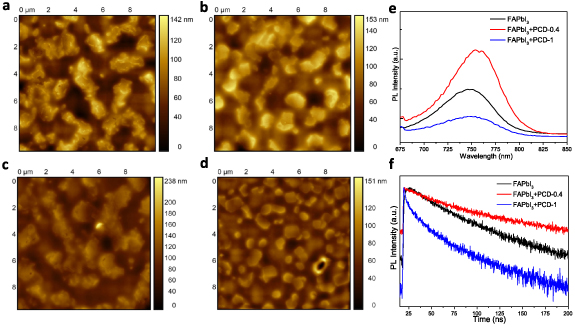
Figure 6. A 10 × 10 μm2 AFM surface topography of FAPbI3 perovskite with two different concentrations of PCDs (0.4 mg ml−1 (a), (c) and 1.0 mg ml−1 (b), (d)) deposited on pristine SnO2 (a), (b) and BDP coated SnO2 (c), (d). (e) Steady-state PL and (f) TRPL decay curves of FAPbI3 perovskite with two different concentrations of PCDs deposited on glass.
Download figure:
Standard image High-resolution imageFurthermore, an increase in the intensity of the steady-state PL spectrum of the perovskite film (coated on glass) with a 0.4% concentration in PCDs compared to the reference film indicates the passivation effect of the polymerized carbon dots (figure 6(e)). However, when inserted in a higher concentration these dots induce large decrease in the PL emission of the hybrid perovskite:carbon dot film. Notably, the UV–Vis absorption spectra of all samples were very similar (figure S7). The same conclusions can be drawn from TRPL decay curves (figure 6(f)) that also suggest a passivation effect of PCD with the lower concentration (i.e. 0.4 mg ml−1). PL and TRPL measurements taken in perovskite samples without and with the carbon dots coated on as-deposited and BDP-modified SnO2 also indicated enhanced charge injection, when using the BDP interlayer, as well as, the passivation effect of PCDs (figure S8).
3.4. PeLED performance
PeLEDs based on FAPbI3 perovskite emissive layers with and without PCD additive (0.4 mg ml−1) using pristine SnO2 or BDP-modified SnO2 were next fabricated. They consisted of the following layers: glass/ITO (100 nm)/SnO2 or BDP-modified SnO2 (40 nm)/FAPbI3 (+AVA) + PCD (50 nm)/poly-TPD (40 nm)/MoO3 (30 nm)/Al (100 nm). The corresponding energy levels of each layer are shown in figure 7(a). By inserting the BDP modification interlayer on top of SnO2, a perfect alignment between the highest occupied molecular orbital of the interlayer and the VB of the perovskite occurs. The insertion of a thin BDP interlayer on top of SnO2 is expected to enhance electron injection and transport within the device.
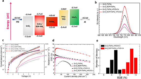
Figure 7. (a) Energy level alignment of different layers used in the device sequence considering vacuum level alignment before contact. (b) The electroluminescence spectra, (c) current density–voltage–radiance characteristics and (d) EQE plotted against the current density of the four types of the fabricated PeLEDs. (e) Device statistics extracted from a batch of 49 devices of each type.
Download figure:
Standard image High-resolution imageFigure 7(b) shows the electroluminescence (EL) spectra of the pristine and modified with BDP SnO2, combined with FAPbI3 and FAPbI3 + PCD emissive layers. The devices showed a peak EL at 770 nm, which is blue shifted compared to the PL maxima (figure S8). There are several reasons that can explain the differences between the EL and PL spectra. PL is mainly determined by the optical properties of the material, while the EL is determined by a number of factors such as the optical properties and physical structures of the optically active layers, the electrical properties of two conductive regions, which are used for cathode and anode contacts, and the properties of the electrical contacts through which the electrical current injected. EL is usually performed on the finished devices (such as LEDs) since it needs a device structure to inject current. As LEDs are multilayer structures with thicknesses on the order of the emission wavelength, EL spectra will depend on both the thicknesses and the refractive indices of the individual layers as a result of interference effects in a 'weak' microcavity [41]. The above parameters will influence the position of the recombination zone hence affecting the profile and intensity of the EL spectrum. Furthermore, other phenomena such as suppression of Auger recombination under external bias has been reported to alter the profile of PL and EL spectra [42].
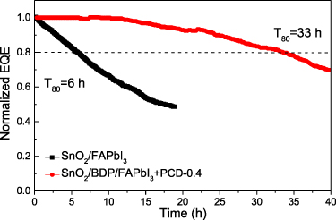
The current density and radiance vs. voltage characteristics show that the devices using the BDP modified SnO2 open at lower voltage compared to the reference ones (based on pristine SnO2), which suggests efficient carrier injection from the modified bottom electrode (figure 7(c)). More importantly, a large improvement in the radiance of the PCD-based PeLEDs was achieved. Especially, in the case of the device based on the FAPbI3 + PCD-0.4 coated on the BDP modifier the measured peak radiance was increased to 92 W sr−1 m−2, representing a large improvement compared to the reference device without PCDs and BDP (2.5 W sr−1 m−2). The device with the FAPbI3 + PCD-0.4 emitter deposited on the pristine SnO2 ETL showed also enhanced radiance of 54 W sr−1 m−2, indicating the beneficial role of the PCD on the device performance. Furthermore, a clear enhancement in the obtained EQE was found, when using the modified ETLs and the PCD PeLED emissive layers. EQE was measured to be 6% and 9% for the FAPbI3 coated on the pristine and BDP modified SnO2 ETL, respectively, which was increased to 10% and 14% for the PCD PeLEDs based on the SnO2 and SnO2/BDP substrates, respectively (figure 7(d)). Table 1 provides a detailed comparison on the current advancement in the FAPbI3 perovskites PeLEDs concluding the performance of our device and recent state-of-the-art PeLEDs [43–54]. The optimized devices also showed reduced efficiency roll-off compared to the reference with no modification and additive (figure 7(d)). They were also quite reproducible as shown by the histograms of the device EQE data extracted from a batch of for 49 devices (figure 7(e)). The synergistic effect of our additive and interface engineering approach also resulted in enhanced device lifetime [55–57]. Figure 8 presents the variation of normalized EQE versus time of continuous operation of a reference PeLED (using FAPbI3 and as-deposited SnO2) and the optimized device based on SnO2/BDP and PCD additive engineering approach. Both devices were biased at a current density of 50 mA cm−2 (initial EQE of 6 and 13% for the reference and champion PeLED, respectively). The estimated T80 lifetimes (the time where the EQE declines to 80% of the initial value) were 6 and 33 h for the reference and engineered device, respectively. This high performance and enhanced lifetime of the PCD PeLEDs is attributed to the passivation effect of PCD and the improved microstructure of the perovskite caused by the BDP and PCDs along with the favorable energy level alignment at the electron injection interface upon the BDP modification of SnO2.
Figure 8. Variation of the normalized EQE of the reference PeLEDs using as-deposited SnO2 and pristine FAPbI3 (with AVA) layers and of the best performing device using BDP and PCDs.
Download figure:
Standard image High-resolution image
Table 1. Performance comparison of PeLEDs based on FAPbI3 emissive perovskite layer.
| Device structure | EQE (%) | Radiance (W sr−1 m−2) | Reference |
|---|---|---|---|
| ITO/ZnO/PEIE/AAC-FAPbI3/TFB/Au | 18 | 286 | [43] |
| ITO/ZnO/PEIE/EDEA-FAPbI3/TFB/Au | 18 | 225 | [43] |
| ITO/ZnO/PEIE/ODEA-FAPbI3/TFB/MoO3/Au | 22.8 | 110 | [44] |
| ITO/ZnO/PEIE/FAPbI3/TFB/MoOx /Au | 19.9 | — | [45] |
| ITO/ZnO/PEIE/BDAFAn −1PbnI3n+1/TFB/ MoO3/Au (n = 6) | 4.7 | 148.9 | [46] |
| ITO/ZnO/PEIE/FAPbI3/PMMA/TFB/MoO3/Au | 19.6 | 875 (at 1500 mA cm−2) | [47] |
| ITO/PEDOT:PSS/TFB/PEF-FAPbI3/TPBi/LiF/Al | 10.7 | 1.27 | [48] |
| Au/MoO3/TFB/FA0.83Cs0.17PbI3/PEIE/ZnO/ITO | 17.5 | 1282.7 | [49] |
| ITO/ZnO/PEIE/NH2-PEG4-NH2-FAPbI3/TFB/MoO3/Au | 19.2 | 360 | [50] |
| ITO/ZnO/PEIE/AEAA-FAPbI3/TFB/MoO3/Au | 22.2 | 93 (at 85 mA cm−2) | [51] |
| ITO/ZnO/PEIE/3Cl-BA-FAPbI3/TFB/MoOx /Au | 16.6 | 300 (at 460 mA cm−2) | [52] |
| ITO/PEIE-ZnO/APS-FAPbI3/TFB/MoOx /Au | 19.2 | 240 (at 3.6 V) | [53] |
| ITO/PEDOT:PSS/VB-FPND/ PEAI2-FAPbI3 QDs/CN-T2T/LiF/Al | 15.4 | — | [54] |
| ITO/SnO2/BDP/FAPbI3 + PCD/TPD/MoO3/Au | 14 | 92 | This work |
4. Conclusions
In conclusion, we have simultaneously modified the surface of SnO2 used as the bottom ETL and the emissive layer in PeLEDs based on FAPbI3. As a surface modifier for SnO2, we used an amino-functionalized BDP, which alters the surface tension, as well as, the interface energetics thus favoring the formation of smaller perovskite domains and reducing the electron injection barrier simultaneously. We also inserted core–shell carbon-polymer quantum dots in the perovskite emitter to passivate bulk defects and further alter the microstructure. As a result, the FAPbI3 PeLEDs showed considerable performance enhancement, reduced efficiency roll-off and enhanced lifetime compared with the reference device without BDP and PCDs. This work suggests that surface modification of charge transport materials and additive engineering of the perovskite emitter represent vital solutions for further advancements in perovskite optoelectronics.
Acknowledgments
This research is co-financed by Greece and the European Union (European Social Fund-ESF) through the Operational Programmed «Human Resources Development, Education and Lifelong Learning» in the context of the project 'Reinforcement of Postdoctoral Researchers—2nd Cycle' (MIS-5033021), implemented by the State Scholarships Foundation (IKΥ).
Data availability statement
The data generated and/or analyzed during the current study are not publicly available for legal/ethical reasons but are available from the corresponding author on reasonable request.
Supplementary data (0.9 MB PDF)