
Abstract
Human beings have witnessed unprecedented developments since the 1760s using precision tools and manufacturing methods that have led to ever-increasing precision, from millimeter to micrometer, to single nanometer, and to atomic levels. The modes of manufacturing have also advanced from craft-based manufacturing in the Stone, Bronze, and Iron Ages to precision-controllable manufacturing using automatic machinery. In the past 30 years, since the invention of the scanning tunneling microscope, humans have become capable of manipulating single atoms, laying the groundwork for the coming era of atomic and close-to-atomic scale manufacturing (ACSM). Close-to-atomic scale manufacturing includes all necessary steps to convert raw materials, components, or parts into products designed to meet the user's specifications. The processes involved in ACSM are not only atomically precise but also remove, add, or transform work material at the atomic and close-to-atomic scales. This review discusses the history of the development of ACSM and the current state-of-the-art processes to achieve atomically precise and/or atomic-scale manufacturing. Existing and future applications of ACSM in quantum computing, molecular circuitry, and the life and material sciences are also described. To further develop ACSM, it is critical to understand the underlying mechanisms of atomic-scale and atomically precise manufacturing; develop functional devices, materials, and processes for ACSM; and promote high throughput manufacturing.
Export citation and abstract BibTeX RIS

Original content from this work may be used under the terms of the Creative Commons Attribution 3.0 licence. Any further distribution of this work must maintain attribution to the author(s) and the title of the work, journal citation and DOI.
1. Introduction
The development of human civilization is linked to the development of tools of progressively finer length scales (figure 1). From the beginning of using stone tools in the Stone Age to metal shaping using casting and forging in the Bronze and Iron Ages, human beings have manually manufactured tools and various supplies over a fairly long period of time with tool sizes in the millimeter range, visible to the naked eye. The invention of the steam engine in the 1760s transformed manufacturing from craftwork into a technology with the invention of a series of steam, water, and mechanical equipment with submillimeter precision. Following the discovery of electricity and the division of labor in the 1870s, machine structure and precision dramatically improved from the macro-to the micro size, enabling interchangeability and mass production. In the second half of the 20th century, the synergy of optics and light-induced chemical reactions formed the basis of photolithography with resolutions down to the submicron and even the nanometer scale, enabling rapid development of microelectronics, information technology, and automated production. Meanwhile, the invention of computer numerical control (CNC) led to a quantitative leap in product performance, enabling submicron and nanometer precision. Today, the development of modern lithography enables electronic circuits and devices to reach 3 nm resolution; and CNC ultraprecision machining ultimately achieves sub-nanometer surface finish with form accuracy down to the nanometer scale. This is where we are at today.

Figure 1. Development of tools with civilization of human beings.
Download figure:
Standard image High-resolution image1.1. What is next?
In 1959, Feynman delivered his famous talk, 'There's Plenty of Room at the Bottom' to the American Physical Society [1]. He asked, 'What would happen if we could arrange the atoms one by one the way we want them?'. 'What would the properties of materials be if we could really arrange the atoms the way we want them?'. These questions inspired the development of nanotechnology. Drexler introduced the fundamental principles of molecular engineering and outlined development paths to advanced nanotechnologies in his paper in 1981 and in a subsequent dissertation [2]. In 1990, nanotechnology became popular with growing investment from governments.
Nanotechnology embraces a wide range of technologies with feature dimensions from 1 ∼ 100 nm [3]. The application of nanotechnology spans many research fields, such as material science, chemistry, semiconductor technology, molecular biology, medicine, etc. However, nanotechnologies do not necessarily require atomic-scale precision. In 2007, Battelle Memorial Institute and the Foresight Nanotech Institute published 'Productive nanosystems: a technology roadmap' to develop atomically precise manufacturing (APM), which is a first attempt to map out the research and development (R&D) pathways across multiple disciplines to achieve atomically precise manufacturing [4]. Atomically precise manufacturing is described as the production of materials, structures, devices, and finished goods in a manner such that every atom is at its specified location relative to the other atoms and in which there are no defects, missing atoms, and extra atoms, according to a recent call by the US Department of Energy [5]. In 2015, in a workshop on Integrated Nanosystems for Atomically Precise Manufacturing in California, the participants identified two specific positional assembly methods for achieving this extraordinary level of precision: (1) tip-based positional assembly using scanning probe microscopes and (2) integrated nanosystems using molecular machine components. However, APM is still largely reliant on macromolecular assembly and lacks important input from mechanical manufacturing. Based on the history of manufacturing development, Fang formally proposed three phases of manufacturing advances [6, 7]:
- Manufacturing I: Craft-based manufacturing by hand, as in the Stone, Bronze, and Iron Ages, in which manufacturing precision is at the millimeter scale.
- Manufacturing II: Precision-controllable manufacturing using machinery where the material removal, transformation, and addition scales are reduced from millimeters to micrometers and nanometers.
- Manufacturing III: Manufacturing objectives and processes directly focused on atoms, spanning the macro- through the micro- to the nanoscale where manufacturing is based on removal, transformation, and addition at the atomic scale, namely, atomic and close-to-atomic scale manufacturing.
Atomic and close-to-atomic scale manufacturing (ACSM) includes all of the steps necessary to convert raw materials, components, or parts into products designed to meet users' specifications. The processes involved in ACSM are not only precise at the atomic level but also remove, add, or transform work piece materials at the atomic and close-to-atomic scale. Atomic and close-to-atomic scale manufacturing provides a fundamental competence for the production of the fourth generation of core elements in contemporary industrialization.
This review is organized based on atomic-level operation modes in subtractive, additive and transformative manufacturing processes. We will discuss ACSM by including processes from ultraprecision machining, micro-/nanofabrication, and macromolecular assembly to tip-based manufacturing. The emerging applications of ACSM will be discussed. Insight into future research in ACSM will be shared as well.
2. Manufacturing approaches for ACSM
2.1. Subtractive manufacturing
Subtractive manufacturing is a process generate three-dimensional (3D) objects by successively removing material away from a solid block of material. Subtractive manufacturing can be done using either manual-based cutting the material or CNC based machining, where CNC is mostly used nowadays. In 1974, Taniguchi, a Japanese precision engineering researcher, defined nanotechnology as a production technology for achieving highly accurate, ultrafine dimensions on the order of a nanometer. He proposed a chart to record and predict improvements in machining accuracy, as shown in figures 2 [8]. As seen in his chart, ultraprecision machining reached subnanometer accuracy in 2000. This was achieved for ultraprecision grinding and polishing of Chandra mirrors with an axial form error of 5 nm root mean square (rms) and roughness of 1.8–3.4 Å rms, as measured over a distance of 0.01–1 mm in 1990 [9]. Today, brittle materials, such as silicon (Si), can readily be turned without brittle fracture with ∼1 nm rms roughness with a limited amount of subsurface atomic bond dislocation, typically approximately 200 nm deep [10]. Comparably, for semiconductor fabrication, Moore's law, published in 1965, predicted that the number of transistors in a dense integrated circuit will double about every two years (figure 3). The number of transistors increased from 2,300 in 1971 to 1.5 billion in 2015. Today, computer processors, such as the recently announced Apple A12 Bionic chip and Huawei Kirin 980, use 7 nm processes with 6.9 billion transistors on a centimeter square chip. The limits are being pushed to 5 nm and even 3 nm nodes [11]. A summary of ultraprecision machining, nanolithography, and other subtractive processes which are promising for atomic and close-to-atomic manufacturing follows.

Figure 2. The general improvement in machine accuracy capability during much of the 20th century, as interpreted based on the Taniguchi curves. Reproduced with permission from [10].
Download figure:
Standard image High-resolution image
Figure 3. Number of transistors on Intel's mainstream microprocessor chip. Reproduced with permission from [12].
Download figure:
Standard image High-resolution image2.1.1. Ultraprecision machining
2.1.1.1. Ultraprecision diamond turning/milling
In ultraprecision machining, there are two main research fields: ultraprecision turning/milling and ultraprecision grinding/polishing. Ultraprecision diamond machining using diamond tools is an efficient way to machine complex form surfaces with a nanometer surface finish and submicrometer and even nanometer form accuracy. As shown in figure 4, there are different ultraprecision diamond machining technologies, including single-diamond turning, ultraprecision raster milling, slide tool servo machining, fast tool servo machining, etc. The cutting depth of diamond tools in ultraprecision diamond machining is critical and determines the minimum amount of materials which can be stably removed from workpiece surfaces.

Figure 4. Different ultraprecision machining processes: (a) single point diamond turning, (b) ultraprecision raster milling, (c) slide tool servo machining, and (d) fast tool servo machining.
Download figure:
Standard image High-resolution imageAs shown in figure 5, Fang et al [13, 14] developed a taper cutting method to study the material removal mechanism from the micrometerscale to the nanometerscale; and they realized stable cutting with a minimum chip thickness of 6 nm. Currently, the surface roughness achieved by ultraprecision diamond machining using diamond tools can be sub-10 nm, i.e. 1 nm arithmetic roughness (Ra) for monocrystal Si (figure 5(b)). This method is still far away from achieving a single atomic layer of material removal.

Figure 5. (a) Schematic illustration of the experimental setup of taper cutting (b) with an inclination ratio of 1:10,000 and a surface finish of monocrystal silicon. Reprinted from [14], Copyright (2005), with permission from Elsevier.
Download figure:
Standard image High-resolution imageIn this paper, the micro/nano cutting mechanism is described as shearing, extruding, or rubbing to explain plastic deformation and surface generation [15]. Material removal at the atomic scale is only demonstrated in molecular dynamic simulation, where single crystallized copper material is used; and the theoretical tool radius is as small as 5 nm [16]. As shown in figure 6, material removal is still not achieved in a layer-by-layer fashion; and clear removal of a single layer of copper is still difficult to achieve. Molecular dynamic simulation is used to simulate the cutting of copper using a single point diamond tool. The accuracy of material removal in ultraprecision machining depends on the precision and accuracy of the machining tool, tool wear, the process, relative displacement between the tool and the workpiece, and the machining environment, such as temperature. Machining accuracy is generally worse than machine accuracy, as the errors of machine tools and the relative displacement of the tool and the workpiece can be transferred to the surface of the workpiece. Since the accuracy of linear motion of the current single point diamond turning machine is tens of nanometers, it is still difficult to cut nanoscale and even atomic-scale layers.

Figure 6. Deformation of a Cu (0 0 1) based on molecular dynamic simulation: (a) when tool edge radius is 5 nm, the scratching depth is −0.21 nm; (b) when tool edge radius is 3 nm, and the scratching depth is −0.13 nm. Reprinted from [16], Copyright (2016), with permission from Elsevier.
Download figure:
Standard image High-resolution image2.1.1.2. Ultraprecision grinding/polishing
Grinding is an abrasive process, where small, nonmetallic hard particles are capable of removing a small amount of material from a surface through cutting processes [17]. As shown in figure 7, ultraprecision grinding is a grinding process for the generation of surfaces with low surface roughness, high form accuracy, and high surface integrity. The material removal mechanism is at the borderline between brittle and ductile transition. In the ductile material removal regime, no to little subsurface damage occurs, while the brittle material removal regime is characterized by cracks and outbreaks [18]. Ultraprecision grinding is used to generate parts with a high surface finish, high form accuracy, and high surface integrity. It is usually used to machine hard and brittle materials, such as ceramics, carbides, glasses, hardened steel, or semiconductor materials. Since it is intrinsically a mechanical machining process, the surface finish can be smaller than 2 nm with little subsurface damage [18]. It is not possible to obtain a surface with atomic-scale precision and surface finish.

Figure 7. Ultraprecision grinding: (a) ultra-precision grinding system, (b) and (c) workpiece surface morphology after ultra-precision grinding.
Download figure:
Standard image High-resolution imagePolishing is usually used as a finishing process to remove subsurface damage from cutting and grinding processes. Ultraprecision polishing integrates mechanical removal and chemical reaction using fine abrasives assisted by soft polishing tools, chemical fluidics, or electric/magnetic fields. Ultraprecision polishing is used to superfinish the surface of the workpiece with no/low surface/subsurface damage. It can achieve submicrometer form accuracy and surface finish in the several nanometer and subnanometer range.
No-damage polishing methods can be categorized into several categories i.e. mechanical microremoval polishing (see figure 8), fluid jet polishing (see figure 9), chemical polishing, and chemical mechanical polishing. The mechanical actions include micro removal, erosion, and friction, while the chemical effects include electrolysis, melting, and film formation. No-contact polishing technologies, such as fluid jet polishing, use polishing pads which do not contact the workpiece. Material is removed by the interaction and impact of the fine particles in the slurry. Elastic emission machining (EEM) is a typical noncontact polishing method in which fine abrasives (tens of nanometers in size) in the slurry are driven by a high-speed, rotating sphere close to the workpiece surface to create flow in the slurry with dynamic pressure at the gap. The abrasives chemically react with the surface to remove material, as shown in figure 10(a). The EEM method, first proposed by Mori et al, was used to polish monocrystalline Si using zirconium dioxide (ZrO2) abrasives achieving a surface roughness of 500 pm [19]. Elastic emission machining was further optimized with a higher removal rate of up to 100 × 10−4 mm3 h−1 with a surface roughness of 85 pm rms [20], as indicated in figure 10(b).

Figure 8. Bonnet polishing.
Download figure:
Standard image High-resolution image
Figure 9. Fluid jet polishing.
Download figure:
Standard image High-resolution image
Figure 10. Principle of elastic emission machining and surfaces (a) before and (b) after processing by EEM. Reproduced with permission from [20].
Download figure:
Standard image High-resolution imageRecently, the Yamauchi group proposed the catalyst-referred etching (CARE) process for polishing the surface of a single crystalline 4H-silicon carbide (SiC) [21]. As shown in figure 11, a catalytic pad is used to perform etching exclusively on the pad surface. The topmost part of the workpiece surface in contact with the pad surface is preferentially removed. The pad surface also acts as a reference pad that is statistically copied onto the work surface. The chemically oriented etching mechanism of CARE thereby smooths the work surface effectively. During CARE, platinum and hydrofluoric (HF) solution are generally employed as the catalyst and etchant, respectively; and the main reaction of this process is a catalytically induced, indirect dissociative adsorption of the HF molecule [22]. As shown in figure 11 (b), a step-terrace structure with a step height of approximately 3 Å was observed using Atomic force microscopy (AFM). Such a step high represents on bilayer thickness of silicon and carbone, which means the material removal is based on chemical phenomena and that a type of step-flow removal occurs on the SiC (0001) Si surface. The roughness of the surface is 0.142 nm rms with a well-ordered crystal structure and is damage free. Moreover, plasma-assisted machining processes, such as plasma chemical vaporization machining (PCVM) [23] and plasma-assisted polishing (PAP) [24], can also be applied to obtain a damage-free surface with flattenability at the atomic level.

Figure 11. (a) Principle of CARE process and (b) AFM image of a CARE-processed surface with a step-terrace structure observed with a step height of approximately 3 Å corresponding to one bilayer thickness of Si and C, generated with a removal depth of 3 μm in 1 μm × 1 μm area; RMS: 0.118 nm (P-V: 2.649 nm, Ra: 0.089 nm) (a) Reproduced with permission from [21]. (b) Reproduced from [22] (2006). With permission of Springer.
Download figure:
Standard image High-resolution imageIn summary, the development of ultraprecision machining technologies, particularly ultraprecision polishing, enables an atomically flattened damage-free surface. However, state-of-the-art ultraprecision machining processes are still unable to reach material removal of a single atomic layer due to the constraints of machine tool precision and cutting tool interaction with the workpiece surface. Atomic-level uniformity over a large area, such as wafer scale, is still challenging. Critically, ultraprecision machining processes can only finish workpiece surfaces and cannot generate atomic-scale features with specific line widths, which has proven to be important in component-level development.
2.1.2. High energy beam machining
2.1.2.1. Focused ion beam
Electron and ion beams are capable of removing material at atomic scale. A liquid metal gallium (Ga) ion beam with a ∼10 nm resolution is a dominatant ion source for etching of nanoscale materials. However, Ga has problems with contamination and is more destructive than the lower mass helium/neon (He+/Ne+) source. The recently developed He+/Ne+ gas field ion source microscope shows that the He+ source has a sub-1 nm resolution [25] and that the Ne+ has a theoretical resolution of 0.25 nm [26]. They were applied for imaging, circuit editing, debugging [27], milling, and deposition. Figure 12 shows a Zeiss ORION NanoFab helium ion microscope column.

Figure 12. Schematic of column of Zeiss ORION NaboFab helium ion microscope with ion source, apertures, Everhart–Thornley secondary electron (E–T SE) detector, and microchannel plate (MCP) detector configuration. Reproduced from [28]. © IOP Publishing Ltd. CC BY 3.0.
Download figure:
Standard image High-resolution imageAs shown in figure 13, enhanced resolution has been realized with focused ion beam milling of Si [29] and strontium titanate (SrTiO3) [30] using a He focused ion beam (FIB). The He-induced area shows a uniform background contrast, implying a more uniform thickness. Additionally, He ion milling has achieved a sub-6 nm resolution, such as plasmonic nanoantennas on a gold (Au) film (figure 14), smaller than 10 nm resolution for Ga milling of bulk materials [31, 32]. However, it is still difficult to achieve single-atom level precision and single-atom scale feature sizes in bulk substrates using ion beam machining.

Figure 13. High resolution transmission electron microscopy (TEM) of Si induced by FIB machining using Ga and He sources: (a) scanning electron microscopy (SEM) and (b) diffraction information from the Ga-finished region. (c) High resolution TEM (HRTEM) and (d) diffraction information from the He-modified region. Reproduced from [29]. CC BY 2.0.
Download figure:
Standard image High-resolution image
Figure 14. 30-nm-thick Au wires milled by a He ion beam with milling pattern widths of 20, 10, and 5 nm, which is used as plasmonic nanoantennas fabricated by He ion milling: Scale bar:100 nm. Reprinted with permission from [32]. Copyright (2013) American Chemical Society.
Download figure:
Standard image High-resolution imageInstead of machining bulk materials, the alternative is to machine two-dimensional (2D) materials, such as graphene and metal dichalcogenides. Such 2D materials are confined with only one and a few atomic thick layers on top of the substrate. Bell et al [28] used a He-focused ion beam to machine graphene on a Si/silicon dioxide (SiO2) substrate, as simulated in figure 15. The simulation shows that the Ga atoms deposit most of their kinetic energy in the most upper parts of the material. This means that the Ga beam is suitable for bulk milling with higher efficiency but with lower resolution. However, He shows less interaction with graphene where 99.6% of the ions pass though the graphene directly; and the majority of the energy is deposited deep within the Si substrate. This means that He has a higher machining resolution with potentially smaller milling feature sizes. Abbas et al [33] used He ion beam machining to fabricate graphene nanoribbon arrays (GNAs) down to 5 nm (figure 16). First, a P2+Si/SiO2 wafer was coated with graphene using chemical-vapor-deposited (CVD). Then, contacts for the source and drain was formed based on patterned titanium (Ti)/Au electrodes. Afterwards, unwanted graphene is removed using oxygen (O) reactive ion etching (RIE) to fabricate a defined channel. Finally, the whole device was loaded into a helium ion beam lithography (HIBL) machine to create the desired graphene nanoribbon (GNR) patterns. The GNRs showed exceptional sensitivity for the detection of nitrogen dioxide (NO2). There are also many research results on machining of graphene using He ion beams to fabricate nanoribbon-based graphene mono-or multiple layers [34–36].

Figure 15. Comparison of simulation result for machining graphene layer on a SiO2 silicon substrate using (a) 30 kV Ga ions and (b) 30 kV He ions, (c) range and trajectory of 30 kV He ions through a suspended graphene layer over vacuum, SiO2, and Si substrate. Insets are molecular dynamics simulations schematic comparison between Ga+ ion and He+ ion interaction with graphene samples. Reproduced from [28]. © IOP Publishing Ltd. CC BY 3.0.
Download figure:
Standard image High-resolution image
Figure 16. Fabrication of GNR arrays using HIBL: (a) schematic diagram HIBL process, and He ion microscope images of (b) 5 nm, (c) 6 nm, and (d) 7.5 nm half-pitch arrays. (e) High aspect ratio GNRs with helium ion microscope image of (width 5 nm, length 1200 nm). (f) A smooth interface between graphene and patterned GNRs, where bright lines represent graphene. Reprinted with permission from [33]. Copyright (2014) American Chemical Society.
Download figure:
Standard image High-resolution imageInstead of graphene, other 2D materials, such as single layers of transition metal dichalcogenides, e.g. molybdenum disulphide (MoS2), also exhibit potential applications in optoelectronic devices, gas sensing, and energy storage based on atomic-scale modification [37]. Fox et al [37] milled a few layers of MoS2 using a He ion beam with probe sizes of ∼12, ∼5.9, and ∼1.7 nm, where the small size led to less damage. When the beam size was optimized to ∼1 nm, a few layers of MoS2 could be milled with nanoribbons. As shown in figure 17, the potential heating effect created amorphous MoS2 during milling as the ribbon size gets smaller.

Figure 17. Freestanding nanoribbons in 2D materials fabricated using He beam machining: (a) a 9-nm-wide crystalline MoS2 nanoribbon; (b) a 5-nm-wide amorphous MoS2 nanoribbon; (c) an amorphous nanoribbon with a minimum width of less than 1 nm; (d) scanning transmission electron microscopy (STEM) image of a 7 nm wide crystalline MoS2 nanoribbon; (e) a 9 nm wide crystalline manganese oxide (Mn2O3) nanoribbon milled with a helium ion microscope (HIM); (f) titanium dioxide (TiO2) edge milled with HIM and (g) an array of 10-nm-wide Mn2O3 nanoribbons milled with HIM. Reprinted with permission from [37]. Copyright (2015) American Chemical Society.
Download figure:
Standard image High-resolution imageOn the whole, we found that instead of Ga+ FIB machining, focused He ion beam machining is becoming a preliminary tool for milling 2D materials, due to its smaller probe size in the subnanometer range, lower ion-beam-induced damage, and no additive deposition. However, the process is still at the several nanometers and up precision level. Removal of several atoms has not been realized as of yet. Moreover, material modification from the ion-beam-induced damage, such as heating and deformation, influences its physical properties and needs to be optimized/controlled for a particular application.
2.1.2.2. Focused electron beam
To fabricate sub-1 nm structures over 2D materials is very challenging. It was believed to be impossible for a MoS2 monolayer, as it is too fragile to withstand the electron radiation. However, Liu et al [38] demonstrated the formation of nanoribbons with a smooth width of 0.35 nm after electron beam radiation by carefully controlling the fracture of the MoS2 monolayer via beam energy and density. Lin et al [39] used electron radiation to generate vacancies and vacancy complexes that can expand into relatively large holes in the scanned regions. Two holes were milled side by side using focused electron beam in the selected hole regions. This will confine a ribbon of monolayer at the designated site, as shown in figure 18. The minimum size of the nanowire is ∼5 Å, and its length can be ∼10 nm. Various transition-metal dichalcogenides (TMDC), including molybdenum sulfide (MoS), molybdenum selenide (MoSe), and tungsten selenide (WSe), have been machined with nanowires of ∼5 Å wide, as shown in figure 19. The atom removal under the electron beam can be related to several mechanisms, such as knock-on effects [40], ionization, and beam-induced chemical etching. The electron knock-on effect refers to fast electron interactions with the nuclei and the electron system in the target, causing atom displacement once the primary beam energy is over the threshold. Ionization is mainly a radiolysis process arising from the inelastic scattering of incident electrons, in which case the degree of damage is usually assumed to be proportional to the energy deposited per unit volume of the specimen [41]. Beam-induced chemical etching uses a gaseous precursor flowing over a substrate in a vacuum chamber, and an electron beam is used to simultaneously to dissociate adsorbates and generate reactive fragments and finally lead to etching or deposition [42]. The atom removal mechanism depends on materials, beam energy, scanning dwell time, etc. Research interest in using atomically focused electron beams in a STEM for modification and manipulation of 2D materials with atomic-scale precision has been growing, and more and more nanostructures with atomic precision have been demonstrated [43].

Figure 18. Fabrication of a ramified Y-junction of MoSe nanowire. (a)–(d) Sequential annular dark field images of the fabrication process. The three holes are patterned using the same method described in the main text. By carefully steering the electron beam to scan only the regions indicated by the white dashed squares in each image, the predesigned ramified junction can be controllably created. The method can, in general, be applied to create other shapes of ramified junctions that connect multiple nanowires by patterning the holes in proper positions and using the controlled scan method. Scale bars: 2 nm. Reprinted by permission from Macmillan Publishers Ltd: Nature Nanotechnology [39], Copyright (2014).
Download figure:
Standard image High-resolution image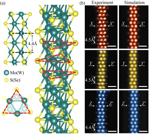
Figure 19. Atomic structure of the nanowire for various transition-metal dichalcogenides: (a) atomic structural model of the nanowire, where dashed red triangles indicate the orientation of each layer in the nanowire, and (b) experimental (left) and simulated (right) STEM Z-contrast images of individual MoSe (orange), MoS (yellow), and WSe (blue) nanowires. Scale bars: 0.5 nm. Reprinted by permission from Macmillan Publishers Ltd: Nature Nanotechnology [39], Copyright (2014).
Download figure:
Standard image High-resolution image2.1.3. Atomic layer etching
As one of emerging technique for fabrication of semiconductor, atomic layer etching (ALE) uses a sequence alternates between self-limiting chemical modification steps to remove only the chemically modified area of the top atomic layer of wafer [44]. The standard example is etching of silicon by alternating reaction with chlorine (Cl2) and etching with argon ions (Ar). In the first step, shown in figure 20, firstly, Cl2 reactants are adsorbed onto the Si film surface; and then excess reactants are purged; following with Ar ions introduced into reaction chamber, silicon chloride byproduct is desorbed via directional ion bombardment; finally, excess gas was purged. Such a process is repeated again and again until the desired amount of material is removed. During the absorption step, a monolayer is expected to form on the to-be-etched surfaces. Hence, no further adsorption occurs. After evacuation of the excess absorbent species, etching happens by the bombardment of ions, energetic neutrals, and others combined with the adsorbed monolayer to form volatile species. Once all species of system are purged, the cycle is then completed. In the case of the reaction step, in figure 20, the reaction only occurs at the surface when an adsorbed species are present, where both absorption and reaction are optimized with material removal rate in one monolayer per cycle. Thus, an atomic finish surface is formed with atomic layer precision without any subsurface damage.

Figure 20. Concept of the four-step ALE process: (a) etchant (reactant) absorption, (b) excess reactant evacuation, (c) energy-induced surface reaction, and (d) reaction production evacuation. Reproduced with permission from [44].
Download figure:
Standard image High-resolution imageThe extension of Moore's law increasingly relies on high-precision fabrication processes to form large-area nanoscale features with high-quality. This is particularly important for the sub-14 nm technology node since transistor performance is highly sensitive to process variations in production [45]. Compared to continuing reactive ion etching (RIE), ALE can reach atomic-layer precision with atomic-scale surface roughness without any subsurface damage, as indicated in figure 21.

Figure 21. Comparison of surface quality epitaxial Si surfaces before etching finished with chemical mechanical planarization, and continuous dry etching and atomic layer etching where they are imaged based on SEM (a) and AFM (b). ALE shows a one monolayer surface finish. Reproduced with permission from [45].
Download figure:
Standard image High-resolution imageThe ALE process has been under development since the 1990s. The process has been applied to Si and hafnium oxide (HfO2) substrates with various reactants and energetic ions for applications of nanoscale transistors in research [44, 46]. However, the greatest challenge with self-limited ALE processes is the capability for controlling adsorption and reaction portion of process. Typically, an absorption layer is formed uniformly on surface of substrate. The reaction is critical, where the threshold energy is tuned to etch only target materials, rather than other reactor materials. However, due to problems of selectivity loss, surface modification, net deposition, and spontaneous etching, ideal atomic precision surfaces are still difficult to achieve.
2.1.4. Atomic force microscope nanomachining
Atomic force microscopy was employed as a single-atom layer removal method for single-crystalline Si. Unlike the conventional uses of AFM probes based on mechanical abrasion, fracture, and deformation, Chen et al [47] developed a new way of using them based on shear-induced mechanochemical reactions under an ambient condition with controlled humidity for single Si atom layer removal. The Si wafer was rubbed away with a 2.5 μm diameter SiO2 microsphere attached to a scanning probe microscope (SPM) cantilever under a pressure of 247 MPa. A 1.4 ± 0.3 Å deep depression was made on a Si (100) surface, which is close to a single Si atom layer of 1.36 Å, as evidenced by the TEM image in figure 22. Atom removal was achieved by shear-induced mechanochemical reactions dependent on water molecular absorption on the topmost layer and counter surface of the tip material. Such a reaction can only happen when a pressure of over 247 MPa is applied, where stress-induced hydrolysis of the Si–Si bonds could occur. The material removal mechanism is explained as shown in figure 23 by: (1) formation of surface hydroxyl species based on reaction of silicon atoms with water molecules (figure 23(d)), (2) interfacial bridge bonding under dehydration reaction between surface hydroxyl groups across the interface (figure 23(e)), and (3), removal of a Si atom from the substrate via breakage of the substrate bonds under the mechanical shear action (figures 23(f) and (g)).

Figure 22. Zero subsurface damage in the mechanochemically etched region: (a) mechanochemical wear region under TME (cross-section); (b) atomic model of Si (100) in the 〈110〉 direction; (c) schematic of atomic step edges after the wearing. Reprinted by permission from Macmillan Publishers Ltd: Nature Communications [47], Copyright (2018).
Download figure:
Standard image High-resolution image
Figure 23. Molecular dynamic (MD) simulation of atomic removal process: (a) sliding MD model; (b) deformation of Si substrate under loading; and (c) removal of Si atoms and release of substrate deformation after unloading. (d)–(g) Mechanochemical-reaction process: (d) formation of silicon hydrogen (Si–H) and Si–OH groups under initial contact; (e) formation of Si1–O–Si4 interfacial bond bridge between Si substrate and silica surfaces, and breaking of Si1–Si3 bond; (f) tensile stress transferred across Si1–O–Si4 bonding bridges; (g) breakage of Si1–Si2 bond for Si atom removal from the Si substrate; (h) and (i) show layer by layer removal process as a function of sliding time under different load conditions. Reprinted by permission from Macmillan Publishers Ltd: Nature Communications [47], Copyright (2018).
Download figure:
Standard image High-resolution imageExcept for mechanochemical-reaction-based AFM, other tip-based nanomanufacturing technologies, such as tip-based nanoelectromachining and tip-based, laser-assisted nonmanufacturing, have been reviewed in the literature [48]. The achievable feature size, however, still ranges from a few nanometers to hundreds of nanometers. Single-atomic layer or single-atom removal has not yet been achieved.
2.2. Additive manufacturing
2.2.1. Atomic layer deposition
Atomic-layer deposition (ALD) is capable of generation of thin films with a variety of materials based on vapor deposition technology. Similar to ALE, it is a sequential and self-limiting chemical reactions. It provides exceptional conformity on high aspect ratio structures with thickness at angstrom level and tenable film composition. ALD has been used in industry with many applications. Figure 24 illustrates the ALD process. The substrate reacts with alternating pules gaseous chemical precursors. This half-reaction is basically carried out used for material synthesis, in which the precursor is pulsed into a chamber under vacuum for a designated amount of time to allow the precursor to fully react with the substrate surface through a self-limiting process that leaves no more than one monolayer at the surface. Any unreacted precursor or reaction by-product are purged with inert carries gas. Followed by the counter-reactant precursor pulse and purge, it allows us to create up to one layer of the desired material. Such process is repeated until the required film thickness is generated [49].

Figure 24. ALD fabrication process: (a) functionalization or treatment of surface with precursor B; (b) reaction with surface with precursor A; (c) purging using inert gas to remove excess precursor and reaction by-products; (d) surface reaction with precursor B; (e) purging with inert carrier gas to remove excess precursor and by-product; (f) cyclic repeating of process for production of surface coatings. Reprinted from [49], Copyright (2014), with permission from Elsevier.
Download figure:
Standard image High-resolution imageAtomic layer deposition offers exceptional conformity, and conformity of high aspect ratio and 3D structures is made possible as chemical reaction is self-limited to surfaces of no more than one layer of precursor. Compared to CVD and physical vapor deposition (PVD), ALD does not suffer from high aspect ratios and shadowing effects, as shown in an example of the deposition of Li5.1TaOz on an aspect ratio of up to 300 anodized aluminium oxide (Al2O3) nanotemplate in figure 25. A variety of materials can be deposited, including metals, insulators, and semiconductors, as reviewed in the literature [49, 50]. Deposits created by ALD are typically less than 1 Å per cycle and achieve an atomic-level smooth surface. The deposition rate is around 3,600 nm h−1 based on a spatial ALD technique. Atomic-layer deposition has been widely used in the fabrication of microelectronic devices, such as high-k and metal gates, n-type metal oxide semiconductor epitaxy (n-MOS epi), and fin field-effect transistors (FinFET). However, as a deposition process, ALD is generally applied to large areas without confinement in line width; and the minimum deposition layer is determined by the precursor's molecule structure.
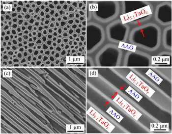
Figure 25. Conformal deposition of Li5.1TaOz deposited by ALD in 300:1 AAO nano template (470:1 final AR). Reprinted with permission from [51]. Copyright (2013) American Chemical Society.
Download figure:
Standard image High-resolution image2.2.2. Macromolecular self-assembly
Self-assembly is a process where pre-existing random components form self-organize structure or patterns upon specific and local interactions between components themselves without any external direction. Here, we are only addressing macromolecular self-assembly, as macromolecules are potential building block materials for APM. According to 'Production nanosystems: a technology roadmap' [4], bio-based APM uses nature, programmable molecules, such as DNA, protein, and biopolymers as feedstocks to produce atomically precise molecular objects. The fundamental mechanism is macromolecular self-assembly based on chemical reaction and biosynthesis on a chemical and biological scale. To make such molecular additive manufacturing happen, feedstocks, their controllable assembly, and precise transport mechanisms with resolution at the atomic scale are required. Currently, protein, peptide, and structural DNA are the most widely used nanomaterials for APM. Structural DNA nanotechnology mostly relies on macromolecular self-assembly, which is the same case for protein engineering. Nonbiological foldamers follows the same principle, but are based on a broader molecular structures and chemical properties [53].
2.2.2.1. Protein assembly
Researchers have expended a lot of effort to study proteins as feedstock building block materials and explored their assembly 'socket.' A breakthrough was made in 2014 with the design of coassembly multicomponent protein nanomaterials in which computational protein modeling and design algorithms were developed. They were not only designed as protein-protein interfaces for directing the formation of novel self-assembly of protein nanomaterials but to provide the energetic driving force for assembly [52]. This means that proteins can be designed to generate two-component nanomaterials with high accuracy and make it possible to design multiple novel interfaces in a single material. This will increasingly enable the construction of more complex materials built from more than two components, as indicated in figure 26. Regarding advanced applications in targeted drug delivery, vaccine design, plasmonic and other applications, design homogeneous protein nanostructures with atomic level accuracy and controlled assembly will be critical and boost further development in these areas. This requires further development of precise patterning from subnanometer to 100 nanometer scale. A more comprehensive review of protein assembly can be found in the literature [53].

Figure 26. (a) Crystal structure of two-component protein nanomaterials designed and (b) confirmation electron micrographs of the two-protein nanomaterial designed. Reproduced with permission from [54].
Download figure:
Standard image High-resolution image2.2.2.2. Peptide assembly
Peptides are short chains of amino acid monomers linked by peptide (amide) bonds. Compared to proteins, peptide contains about 50 or fewer amino acids [54]. α-helices and β-strands are predominant in peptide materials based on secondary structural elements arrangement from hydrogen bond pattern. A peptide material is thus assembled from one or more types of building blocks (of the same secondary structure). Based on its predominant propagation mode (longitudinal, lateral, or both), the topography of the assembly will be defined according to building blocks. Eventually, it forms liner or anisotropic (fibre or tube) or orthotropic structures (figure 27) [55]. Assembly stimuli and their assembly mechanism are still under exploration [56]. Current progress and relevant applications are reviewed in [55, 57, 58].

Figure 27. Peptide secondary structural elements and their assembly into different forms: (a) α-Helix and β-strand protein folding elements and (b) topographies of self-assembly peptide (linear and orthotropic) in relation to sequence, folding and material forms. Reproduced from [55] with permission of The Royal Society of Chemistry.
Download figure:
Standard image High-resolution image2.2.2.3. DNA assembly
DNA molecules have been used as molecular building blocks for nanoscale structures and devices for over 30 years. Nucleic acids are used as nonbiological engineering materials for nanotechnology rather than as the carrier of genetic information. Due to nucleic acid restrictive base pairing rules, the rational design of base sequences allows the formation of target structures with precisely controlled nanoscale features. A variety of convenient design rules and reliable assembly methods have been developed to engineer DNA nanostructures of increasing complexity, as shown in figure 28.

Figure 28. Nanostructure motifs: (a) helical structure of DNA motifs with periodic 2D arrays and 3D crystal: double-crossover DNA tile [63], 4 × 4 DNA tile [64], 6 × 4 DNA tile [65], and tensegrity triangle DNA tile [66]. (b) DNA origami nanostructures: 2D DNA origami smiley face [67], 3D DNA origami in the shape of a gear [68], curved single-layer 3D origami in the shape of a vase [69], and DNA origami gridiron [70]. (a) (Left to right) Reprinted by permission from Macmillan Publishers Ltd: Nature [63], Copyright (1998). Reproduced with permission from [64]. Reprinted with permission from [65]. Copyright (2006) American Chemical Society. Reprinted by permission from Macmillan Publishers Ltd: Nature [66], Copyright (2006). (b) (Left to right) Reprinted by permission from Macmillan Publishers Ltd: Nature [67], Copyright (2006). Reproduced with permission from [68]. Reproduced with permission from [69]. Reproduced with permission from [70].
Download figure:
Standard image High-resolution imageThe four bases present in DNA are adenine (A), cytosine (C), guanine (G), and thymine (T). For nucleic acids, two molecules can only bind to each other to form a double helix structure when the two sequences are complementary. This means that to form the matching sequences of base pairs, A only binds to T and C only binds to G. The sequences of bases in a system of strands thus determines the pattern of binding and the overall structure in an easily controllable way. For example, as shown in figure 29, tensegrity triangle of a rigid DNA motif shows threefold rotational symmetry, with unique strands in magenta (strands restricted to a single junction), green (strands that extend over each edge of the tensegrity triangle), and dark blue (one unique nicked strand at the center passing through all three junctions). Arrowheads indicate the three ends of the strands. The optical image of DNA crystals indicates such self-assembled 3D crystals are macroscopic objects with dimensions exceeding 250 μm. Such large crystals present atomic precision because of the restrictive base pair rules. By designing of base sequence, complex target structure will be formed with precisely controlled nanoscale feature. These structures can be assembled based on tile-based structure assemble from smaller structures, folding structure using DNA origami method, and dynamically reconfiguration structures using strand displacement methods, as seen in some review papers [59–62].

Figure 29. DNA self-assembled tensegrity triangle unique strands organization and optical image tensegrity triangle crystals. Reprinted by permission from Macmillan Publishers Ltd: Nature [66], Copyright (2009).
Download figure:
Standard image High-resolution image2.2.3. Positioning directed assembly
No matter whether it is a supramolecular assembly or structural DNA, protein engineering, or even chemical synthesis, self-assembly faces a problem of encoding in complex components. For example, the biggest challenge for structural DNA engineering is the high error rate of self-assembly [59]. Another potential challenge is scale up. Positional control of assembly can potentially circumvent these constraints. It is clear that for positioning-directed assembly, both atomically precise building blocks and positioning systems are needed. In terms of scale up, high frequency operation is needed. According to the review, protein, peptide, structural DNA, and spiroligomers can be building materials. Their transport mechanism, such as collection and release, are important to explore. The position-based assembly approach, such as the site-specific operation using site-activation tools, e.g. catalyst and paring, needs to be further explored. To position such building blocks, atomically precise positioning is required with high frequency for scaleup.
In 2003, Zettl's Group at Lawrence Berkeley Laboratories and UC Berkeley fabricated the smallest-known nonbiological nanomotor. Such nanomotor used a multiwalled carbon nanotube as a bearing for the rotor and as an electrical conductor [71], as shown in figure 30. A multiwalled carbon nanotube (MWNT) will act as a support shaft for a metal plate rotor (R) and it also works as source of rotational freedom. By integrating with a Si chip, the electrical contact is made via the entire actuator assembly. Since it is electrically driven, macroworld control can be applied. Up-to-date nanomotors based on various energy sources, including biochemical, optical, magnetic, and electric field, have been developed. However, as reviewed in the literature [72], current nanomotors mostly demonstrate rational moment of nanoparticles in suspensions, which cannot deliver force or torque. Their structures are still quite simple, and reliability is poor. To develop an atomic positioning system with high efficacy is still a very challenging task and needs continuous development.

Figure 30. Nanoelectromechanical system (NEMS) actuator with concept design (a) and SEM image prior to HF etching (b). Scale bar: 300 nm. Reprinted by permission from Macmillan Publishers Ltd: Nature [71], Copyright (2003).
Download figure:
Standard image High-resolution imageIt is worthwhile to note that dip-pen nanolithography (DPN) uses the positioning-directed assembly approach. DPN is microscopy-based, scanning probe nanofabrication technology by combining direct-writing and soft-matter compatibility with high resolution. It is a powerful tool to deposit soft and hard materials with high resolution up to sub-50 nm with a variety of stable and functional architectures. DPN has been employed to deposit various materials, including small organic molecules, polymers, DNAs, proteins, peptides, metal ions, and nanoparticles. Generally, molecular inks are coated onto a DPN tip and are delivered to the surface through a water meniscus, as shown in figure 31(a). The coating process is done by either vapor deposition or by dipping the tips into a diluted molecular ink solution. The deposition rate depends on the diffusion rate of the molecules. The feature size is controlled by tip/surface dwell time and the size of the water meniscus. Although AFM scanning is a low throughput process, recent developments of multi-tip, parallel, high throughput, and large-area capability of DPN will open new ways to scale up (figure 31(b)). Combining DPN with molecular building blocks for atomically precise fabrication is expected, unless transport methods, assembly mechanism, and positioning accuracy are properly resolved.

Figure 31. Classic DPN mechanism: (a) molecular ink diffusing from a nanoscale tip to a surface through a water meniscus and (b) high throughput DPN using multiple tips. Reproduced with permission from [73].
Download figure:
Standard image High-resolution image2.3. Transformation
Transformation, in the macro world, indicates material deformation and shape change. In the atomic-scale world, it means atom migration from one location to another. For ACSM, there are three methods of transforming single atoms, i.e. methods based on scanning tunneling microscopy (STM), AFM, and STEM.
2.3.1. STM-based methods
It is well-known that researchers at IBM first manipulated xenon (Xe) atoms on a nickel (Ni) substrate with many single atoms arranged as 'IBM' [74] (figure 32). Since then, STM has become a well-known tool for manipulation of single atoms. In an STM, a tungsten (W) or platinum–iridium (Pt-Ir) alloy conducting tip with an atomic sharpness is brought within a few atomic diameters (Ø1 nm) from the workpiece surface under investigation [75]. Scanning is carried out without any physical contact. A small bias voltage in the mV range is applied, when a conducting tip is brought close to the workpiece surface, which allows electrons to tunnel through the vacuum between them. This is so-called 'quantum tunneling.' Due to high sensitivity of tunneling current exponentially changing with tip-sample distance, tiny distance less than atomic length can be measured [76]. It is extremely sensitive for small changes measurement for individual atoms and their clusters. Due to its high sensitivity (typically 0.005 nm) to gap width, the tunneling current is used as a feedback signal to control gap. When the tip is scanning across the surface with the current sensed, the topography of the surface can be measured in two ways. With constant current, the tip height is adjusted by the feedback loop, where the topography image is obtained via computer imaging software in terms of tip height versus the x and y coordinates. In contrast, in the height mode, the current is recorded as a function of the x and y coordinates [77]. The typical STM configuration is shown in figure 33.

Figure 32. Manipulation of Xe atoms on a Ni (110) surface using STM. Reprinted by permission from Macmillan Publishers Ltd: Nature [74], Copyright (1990).
Download figure:
Standard image High-resolution image
Figure 33. Schematic illustration of STM. Reproduced from [75] (2013). With permission of Springer.
Download figure:
Standard image High-resolution imageThe tip-sample interaction is sensitive to l proximity location of STM-top and surface, which allows for the manipulation of single atoms or molecules one by one [74, 78–80]. It thus allows the measurement of physical/chemical properties of atoms/molecules, which are elusive to other experimental measurements and provides access at the atomic level [81–83]. These functionalities have been reviewed in several literature sources [84, 85].
STM can be used to manipulate atoms in parallel and vertical ways, where parallel process occurs along directions parallel to the surface, and it is so called 'lateral manipulation (LM)'. Vertical manipulation (VM) takes place in surface normal direction. As descripted in [84], the LM of individual atoms generally has three experimental steps (figure 34(a)):
- (1)Approach of the tip toward the atom
- (2)Lateral movement of the STM tip along the surface
- (3)Retraction of the tip back to an image height

Figure 34. Schematic illustration of the STM single atom operation mode: (a) and (b) lateral manipulation and (c) and (d) vertical manipulation mode. Reproduced from [84]. © IOP Publishing Ltd. CC BY 3.0.
Download figure:
Standard image High-resolution imageThe force between tip and atom (the total force Ft) increases, when STM tip approaches atoms adsorbed on a surface (figures 34(a) and (b)). Once required force strength is reached, the tip approach is finished. The tip is then laterally moved along the defined path to a final destination at which the atom will be repositioned. In this process, tip-atom distance is fixed with current constant during operation. Eventually, when atom is brought to the target location, the tip retracted back to the normal image height and the atom remains on the surface.
Vertical manipulation of atom is similar to loading and unloading process of a crane, where the atom is picked or dropped using STM tip. Here the STM tip approaches the atom until a physical contact is made. Potential distribution shows a 'W' shape for initial tip and surface binding sites, as shown in figure 34(c). One well is located on the surface while the other is at the tip's apex [86, 87]. The W-shaped potential can be changed to a single potential well when the tip contacts the surface. STM tip can absorb an atom from the workpiece surface to the tip apex, due to stronger tip-atom binding than atom-surface binding. Applying tunneling current or potential bias or a mechanical movement of the tip often enables the transfer of an atom from the tip apex to the surface [84]. The detailed force analysis and relevant applications can be can be found in several published books [88, 89].
Thanks to STM's ability to manipulate a single atom, STM is now the predominant tool for developing an atomic-scale structure for studying quantum phenomena, such as quantum corrals [90] and electron resonators [91], and inducing chemical reactions at the single-molecule level [92]. Additionally, STM is also used as an APM tool for the fabrication of quantum devices such as a single-atom transistor, by Simmons and co-workers [93], which is the first time a Si-based, single-atom transistor was built from the bottom up. This single-atom transistor was fabricated using a combination of STM and hydrogen-resist lithography. The Si surface was covered by a layer of hydrogen (H). Scanning tunneling microscopy was used to remove the H from specific regions of the surface. The wafer's surface was then exposed to phosphine (PH3) that can only bind with the surface at locations where the H is removed. Finally, a fresh layer of Si was growing on nanostructure surface for encapsulation, where it keeps phosphorus (P) atoms in position and protect them from exposure to the environment. This method has been used not only for prototypes but also for functional electronic devices, including quantum dots [94] and conducting wires [95].
As shown in figure 35, STM single-atom manipulation is a low throughput process; but STM-based single-atom operation combines imaging and patterning and offers a high degree of operational control. However, the manipulation of atoms/molecules requires sophisticated instruments for control of the tip-sample interaction. Scanning tunneling microscopy requires extremely clean stable surfaces, sharp tips, excellent vibration control, and sophisticated electronics. Scanning tunneling microscopy can only be used to scan less easily oxidized, well conductive samples, where ultrahigh vacuum is usually required.

Figure 35. AFM images of single atom transistor with deterministic positioning of a P atom in epitaxial Si: (a) 3D view and (b) 2D view. Reprinted by permission from Macmillan Publishers Ltd: Nature Nanotechnology [93], Copyright (2012).
Download figure:
Standard image High-resolution image2.3.2. AFM-based methods
Although STM is the primary tool for manipulating single atoms, it still has limitations: (a) the sample has to be conductive, (b) an ultrahigh degree of vacuum is needed to prevent the metal from oxidizing, and (c) most of the atomic and molecular designs require cryogenic temperatures [96]. Atomic force microscopy is an obvious alternative to STM in terms of single-atom manipulation.
Atomic force microscopy is a scanning probe microscope where the interaction force between a sharp tip and a sample is used for imaging. Figure 36 shows the principle of an AFM. The sharp tip, with a diameter of atomic sharpness, is fixed at the end of a probe cantilever. The extent of interaction between the sample surface and the tip is measured via cantilever displacement, which is detected by a position sensitive photodiode (PSPD) from a reflected laser beam from the cantilever beam. Atomic force microscopy generally has three operating modes: contact, noncontact, and tapping. In contact mode, the cantilever tip comes into contact with the sample surface. The force between the sample and tip is directly proportional to the displacement and the force constant of the cantilever. The force, or height, is kept consistent; and the laser beam reflection, or the scanning voltage, is measured to be converted into an image. In the noncontact mode, the tip is oscillated at its resonant frequency by an actuator. When the tip approaches the sample surface at about 30–150 Å, the van der Waals interactive force causes changes in both the amplitude and the phase of the AFM probe vibration. Combined with the system's feedback loop, a constant oscillation amplitude, or frequency, is maintained by adjusting the average tip-to-sample distance, which measures the tip-to-sample distance at each (x, y) data point and allows the scanning software to construct a topographic image of the sample surface. In the tapping mode, the tip oscillation is then moved toward the sample until the AFM tip lightly touches or taps the surface. The reduction in oscillation amplitude from the tip touching is used to measure the surface.

Download figure:
Standard image High-resolution imageSimilar to STM, AFM has two operating modes in terms of atom manipulation: (1) lateral and (2) vertical. Atomic force microscopy is generally working in the tapping mode, and the tip-surface interaction force includes the van der Waals force, the electrostatic force, and the magnetic-dipole interactions in a vacuum condition. Sugimoto et al [98] first developed a manipulation approach for single atoms. They substituted tin (Sn) adatoms on germanium (Ge) (1 1 1)-c (2 × 8) surfaces by lateral manipulation of the Sn adatom. First, the AFM scanning direction was aligned (arrow in figure 37(a)) with the vector of the Sn adatom and the first neighboring Ge adatom used a slow tip scan. Then, the tip-surface distance was reduced in successive topographic line scans as the attraction force increased between the outermost tip apex and the atom at the surface. Once the threshold force for substitutional Sn and Ge adatoms was overcome, the Sn adatom followed the motion of the AFM tip (figure 37(b)) and completed the interchange (figure 37(c)). In the vertical manipulation mode, as discovered by Sugimoto et al [99], when the AFM tip gradually approached the surface, there was a threshold interaction at which the energy barriers for the interchange of the closest tip and surface atoms. Once the threshold was reduced below a certain value, it allowed a thermally activated interchange of Sn and Si atoms at room temperature. This was different from STM, where an atom weakly bonded onto a metallic surface can be reversibly transferred between the tip and the surface by applying an appropriate bias voltage, and it requires high level vacuum and ultra-low temperature.

Figure 37. AFM tip based lateral manipulation for substitutional Sn adatoms on a Ge surface: (a) surface image before tip activation of interchange between Sn and Ge adatoms; (b) surface scan with the line connecting the centers of the adatoms, and (c) image for relocation of Sn adatom without perturbing the adatoms. Reprinted by permission from Macmillan Publishers Ltd: Nature Materials [98], Copyright (2005).
Download figure:
Standard image High-resolution imageThe vertical manipulation method significantly decreases operation time needed to create similar atomic patterns by almost a factor of ten. Only 1.5 h are needed, most of which was imaging time for building the structures shown in figure 38. Compared to STM, AFM is able to engineer complex atomic patterns of strongly bound atoms at heterogeneous semiconductor surfaces at room temperature. In addition, AFM single-atom manipulation can be applied to nonconductive materials as well, such as calcium fluoride (CAF2) [100]. A comprehensive review was done by Custance et al [96] that summarized AFM for atom manipulation. Although still in its early stage development, atom manipulation with AFM has demonstrated tremendous potential for exploring the fundamental properties of matter at the nanoscale.

Figure 38. Atomic force microscopy tip controls the vertical manipulation of a Sn-Si atoms exchange: (a) Vertical interchange of the interacting atoms [99] to enable one to (b) 'write' and (c) 'erase' atomic markers. Atom manipulation to form patterns with AFM at room temperature (d) with complex contacts between tip and surface [96]. (a) Reproduced with permission from [99]. (d) Reprinted by permission from Macmillan Publishers Ltd: Nature Nanotechnology [96], Copyright (2009).
Download figure:
Standard image High-resolution image2.3.3. STEM-based methods
A STEM is based on combination of the principle for TEM and SEM. Unlike conventional TEM, where images are formed by electrons passing through a sufficiently thin sample, STEM scans sample with a very finely focused beam of electrons in a raster pattern. The signal generated from the interaction between beam electrons and sample atoms is correlated with beam position to build a virtual image. The grey level at the corresponding location in the image represent location. Compared to conventional SEM, STEM significantly improve in spatial resolution at around 0.2 nm for imaging at the atomic level [101]. The main components of an aberration-corrected STEM are shown in figure 39. The electrons are accelerated from a source and focused into a point on the specimen by a set of condenser lenses and an objective lens. The electron scan is carried out by scanning across the sample using a set of scan coils. The parallel collection of different signals from a variety of detectors can be used to form an image in series with bright field, annular dark field, and high-angle annular dark field with resolution down to the atomic scale.

Figure 39. Schematic of a STEM equipped with an aberration corrector. Reproduced with permission from [102].
Download figure:
Standard image High-resolution imageFigure 39 shows the schematic for an aberration-corrected STEM. With help of a set of condenser lenses and an objective lens, electrons are accelerated and focused onto a position of a specimen. An objective aperture limits the maximum angle of illumination included in the incident probe, which is scanned across the sample by a set of scan coils.
Except for imaging, STEM has also been employed as a tool for manipulation of single atoms. Susi et al [103, 104] used a Nion UltraSTEM™ 100 operated at 60 kV in near-ultrahigh vacuum (2 × 10⁻⁷ Pa) to manipulate Si atoms in monolayer graphene. As shown in figure 40, they first used the STEM to identify a clean area of monolayer graphene with one or more embedded Si atoms. Then, the electron beam was positioned on top of a selected C neighbour to Si. After irradiation for a certain time (typically 15 s), one image was captured to detect the atom location. Occasionally, once sufficient impact coming from electron beam is achieved, Si and C switches places in the lattice. Irradiation of correct atom can be achieved via manual alter location when atom shifted. Such procedure was repeated iteratively to move the atom through the lattice. However, as they have stated, the degree of control over atom movement was still not as good as in STM due to the following issues: (1) it is not determined to changes in structure when placing the beam on the C atom towards where the Si was aiming to move; (2) potential problem of C knocked out during irradiation; (3) less control of Si movement during operation, which can jump in either the wrong direction or over several lattice sites between the captured frames. Recently, Dyck et al [105] introduced Si substitutional defects and defect clusters into a graphene lattice through electron beam scanning from Si source material into pristine graphene or by irradiation of the graphene lattice and source material creating vacancies in the graphene lattice for potential sputtered Si atoms. They subsequently used an electron beam to manipulate the Si defects introduced using controlled scan areas or direct stationary beam irradiation to induce movement. Figure 41 shows how the Si forms a Si timer or tetramers and induces bond rotation.

Figure 40. Manipulation of Si impurities in graphene using STEM electron beam. (Top) Manipulation process illustration. (Bottom) Experiment. The Si impurity was relocated from one site to another. (Top) Reprinted from [102], Copyright (2017), with permission from Elsevier. (Bottom) Reproduced from [106]. © IOP Publishing Ltd. CC BY 3.0.
Download figure:
Standard image High-resolution image
Figure 41. Manipulation of Si dimer from electron beam irradiation: (a) initial configuration, (b) a bond rotation, (c) after bond rotation, (d) a Si adatom temporarily attaching to the defect. The adatom was knocked away and we return to the configuration shown in (e) which appears identical to that in (c). (f) An adatom is recaptured and incorporated into the lattice. Repeated operation through electron beam manipulation (g)–(j). [105] John Wiley & Sons.
Download figure:
Standard image High-resolution imageHowever, the manipulation of single atoms using STEM is still in the very early stages, but it provides an alternative option for single-atom operation in addition to STM and AFM. Since the properties of materials are determined by their chemical structure, single-atom manipulation can be a powerful tool for understanding the atomic-scale physics of materials.
3. Measurement and evaluation
Atomic and close-to-atomic scale refers to both atomic-scale features and atomic-precision structures, which require measurement methods down to the single-atom level. Currently, STM, AFM, and TEM/STEM are the only tools capable of measuring and evaluating ACSM-fabricated components. In section 2.3, transformation-based ACSM was introduced using STM, AFM, and STEM, as they are capable of imaging and manipulating single atoms. The principle of these instruments is not repeated here. Instead, a comparative summary of the characteristics of STM, AFM, and STEM for the measurement and evaluation of ACSM-fabricated components is provided, as detailed in table 1.
As single-atom manipulation and atomic-level image are combined in STM, AFM, and STEM, it is possible to carry out single-atom manipulation. Compared to conventional manufacturing processes, measurements can be separated from the manufacturing processes, which appears to be impossible for single-atom-based manipulation.
4. Applications
Applications are critical to drive the development of technologies and fundamental science of ACSM. The research into ACSM is motivated by either single-atom-based devices or complex nanosystems with atomic-level precision. Although single-atom manipulation started in the 1980s, researchers have not achieved much success in creating single-atomic components. In terms of nanosystems, researchers are still struggling to create commercial nanosystems with atomic-level precision. Until now, the most successful process of ACSM is atomic-layer deposition, which provides controllable and conformal thin films at the Angstrom level. It has been widely used in the energy conversion industry (photovoltaics, fuel cells) [109, 110] and the semiconductor industry (high-k transistors) [111, 112], as one of the process chains integrated into existing product production. However, the development of ACSM has the potential to broadly influence human life, from fundamental materials, life science, agriculture, and information technologies, with the potential to revolutionize production [113]. We are still in the infancy stage of development of ACSM and starting to explore the fundamental science behind the operation of atoms/molecules with atomic precision with limited availability of atomic devices. This section will discuss a few achievements in atomic-level devices in the area of nanoelectonics.
4.1. Quantum computers
Quantum computers are believed to have higher the computational efficiency of ordinary classical machines due to quantum algorithms for the execution of certain tasks with fewer steps. With the development of quantum algorithms and the discovery of quantum error-correcting codes, quantum computers are becoming an increasingly interesting topic [114]. One of the earliest concepts for the development of solid-state quantum computers was using arrays with P atoms in a Si crystal, which provided two nuclear spin states with a basic quantum bit (qubit). Such a device was implemented based on dopants in Si [114]. The introduction of these dopants into Si relies on low energy implantation [115] or in-diffusion from highly doped contact regions [107, 116]. However, the position accuracy of dopant is ∼10 nm, while the implementation of a quantum device requires positioning an individual P atom into Si with atomic precision [93, 117].
Scanning tunnelling microscopy has been realized as a single-atom manipulation tool and was used to position P dopants with atomic precision. In this process, P dopant atoms were manipulated with atomic precision by using STM-based lithography on H passivated Si (100) surfaces to control the adsorption and subsequent incorporation of single P dopant atoms into the Si (100) surface [93, 118–120]. As shown in figure 42(a), the surface of Si (100) was first heated to 1,250 °C for one minute to clean the surface. Atomic H for dosing was created by cracking molecular H with 1,500 °C until the Si surface was saturated. Scanning tunnelling microscopy working under ultrahigh vacuum was used to desorb an H atom with the tip based on an applied-potential basis to form a pattern with atomic precision. Then the PH3 molecules were introduced to the STM-patterned, H-terminated Si (001) surfaces. Due to lower annealing temperature for P atom incorporation compared to H-desorption temperature, the H-resist layer effectively blocked any surface diffusion of P atoms before their incorporation into the substrate surface. Thanks to dissociation of three PH3 molecules within the three-dimer site into PH2+H under high does rates, further reaction is prohibited. The PH2 fragment was recombined with a hydrogen atom and desorb after heating surface to 350 °C. The resulting availability of one free Si site enabled the immediate dissociation of another PH2 to PH+H. Until the final PH2 recombined with H, the remaining PH is dissociate to P. Finally, the P atom was subsequently incorporated into top layer of Si surface at 350 °C by ejection of a Si adatom. STM hydrogen lithography has been adapted to fabricate atomic-scale Si device and was developed to be connected with multiple voltage and current leads to each device by developing a novel strategy to realize true 3D atomic-scale devices [121]. As a result, a couple of quantum devices have been fabricated based on STM H lithography, as shown in figure 43.
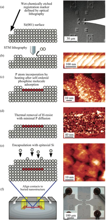
Figure 42. Hydrogen-resist lithography for incorporating single-atom P dopants into a Si surface (100). (Left) (a)–(e) Cross-sectional schematics of fabrication steps with (f) 3D sketch of the final device. (Right) Corresponding (a) STM tip aligned to registration markers, (b) STM images of P incorporated wires, (c) before and (d) after H resist removal, and (e) 25 nm molecular beam epitaxy Si overgrowth, concluding with (f) an optical microscope image of the final device with contact wires. Reprinted with permission from [121]. Copyright (2004) American Chemical Society.
Download figure:
Standard image High-resolution image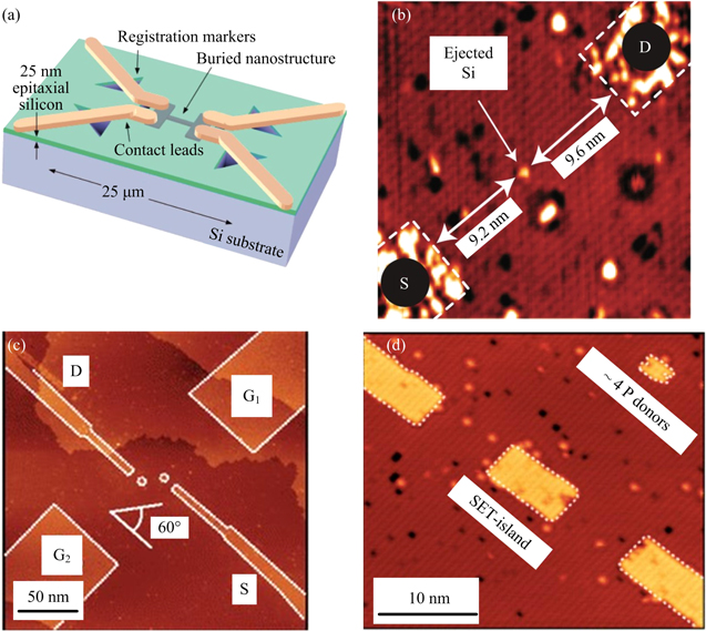
Figure 43. Single atom based device: (a) a 90 × 900 nm2 quantum wire [121]; (b) single atom transistor [93]; (c) two Si:P quantum dots [122] and (d) a single-electron transistor (SET) [123]. (a) Reprinted with permission from [121]. Copyright (2004) American Chemical Society. (b) Reprinted by permission from Macmillan Publishers Ltd: Nature Nanotechnology [93], Copyright (2012). (c) Reprinted with permission from [122]. Copyright (2012) American Chemical Society. (d) Reprinted with permission from [123]. Copyright (2011) American Chemical Society.
Download figure:
Standard image High-resolution image4.2. Life sciences
Cells are information-rich, sophisticated machines with atomic-level assembly precision. Unlike Si-based quantum computers, positioning of single-atom dopants is critical. Structural DNA protein engineering requires atomically precise assembly and control. Due to the strict pairing rule for DNA strands, DNA can be programmable; but such control is not as accurate as in nature. It requires ACSM to push the boundary to the atomic level. In contrast to DNA, RNA and proteins have more refined architectures with atomic-level features. Progress has been made to explore the assembly of interfaces of various proteins and to understand the underlying mechanisms. Such work could make a series of applications possible, such as molecular and cellular biophysics, biomimetic systems, energy transfer and photonics, diagnostic, and therapeutics for human health [59]. For example, DNA structures can be used to build disease-targeting units for diagnostics and therapeutics. The DNA is designed to be a hollow cage into which multiple pharmacological species can be directed. Based on DNA computing, DNA structure can be used as a vehicle to detect disease markers and release drugs based on external stimuli. Such strategy has been realized by Douglas et al [124]. They developed logic-gated nanorobots to transport molecular payloads to cells, sense cell surface inputs for condition triggered activation, and reconfiguration of its structure for payload delivery (figure 44). To assemble DNA nanostructures to form functional devices requires precise control of their relative orientation and position and integration of proteins for DNA computing [125], where site-specific control of assembly can be important to enable such a precision arrangement. However, researchers have shown that structured DNA nanostructures have the potential to precisely deliver drugs into target cells. It is still challenging to transfer DNA nanostructures from mere curiosities into real-world solutions, as the cost of synthetic DNA is very high as is the error rate of self-assembly [59, 125]. Directed assembly of macromolecules, such as DNA, protein, and peptide, is promising to add additional control for forming complex, atomically functional structures.

Figure 44. Design and TEM analysis of aptamer-gated DNA nanorobot: (a) nanorobot loaded with a protein payload; (b) aptamer lock mechanism; (c) perspective view of nanorobot opened by protein displacement of aptamer locks; (d) payloads loading inside the nanorobot; (e) assembly of a nanorobot to 97.5% yield in closed state as assessed by manual counting; and (f) TEM images of robots in closed and open conformations. Reproduced with permission from [124].
Download figure:
Standard image High-resolution image4.3. Ultrahigh-performance materials
As in early science fiction, writers have described ultrahigh-performance materials called 'monomolecular wire' for cutting through glass, metal, and flesh and for building space elevators [126, 127]. Building such strong materials is challenging. If we look at the materials around us, their strength is far below their estimated values, as shown in figure 45. This is due to material defects, such as voids, cracks, and dislocations in the lattice structure, etc. Therefore, there is still a large opportunity to increase material performance. For example, Szlufarska et al [128] demonstrated a precise atomic mechanism to give the 'nanostructured' ceramic material, SiC, both exceptional hardness and ductility, thanks to the crossover that arises from the interplay between cooperative grain sliding, grain rotations, and intergranular dislocation formation, similar to stick-slip behavior. Their molecular dynamic study indicated that the estimated hardness of n-SiC of 39 GPa is in agreement with experimental values of 'super hardness' of 30 to 50 GPa for grain sizes of 5 to 20 nm. As a result, the control of a material's nanostructure will not only improve its performance but potentially provide additional material properties. However, current ACSM is still limited in terms of the range of materials that can be improved.

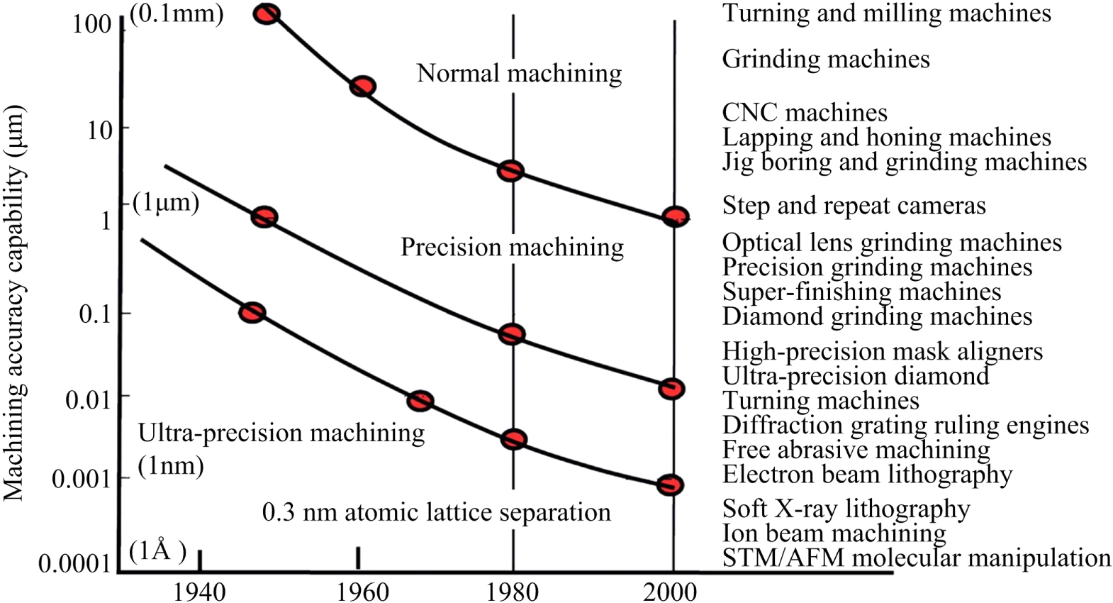
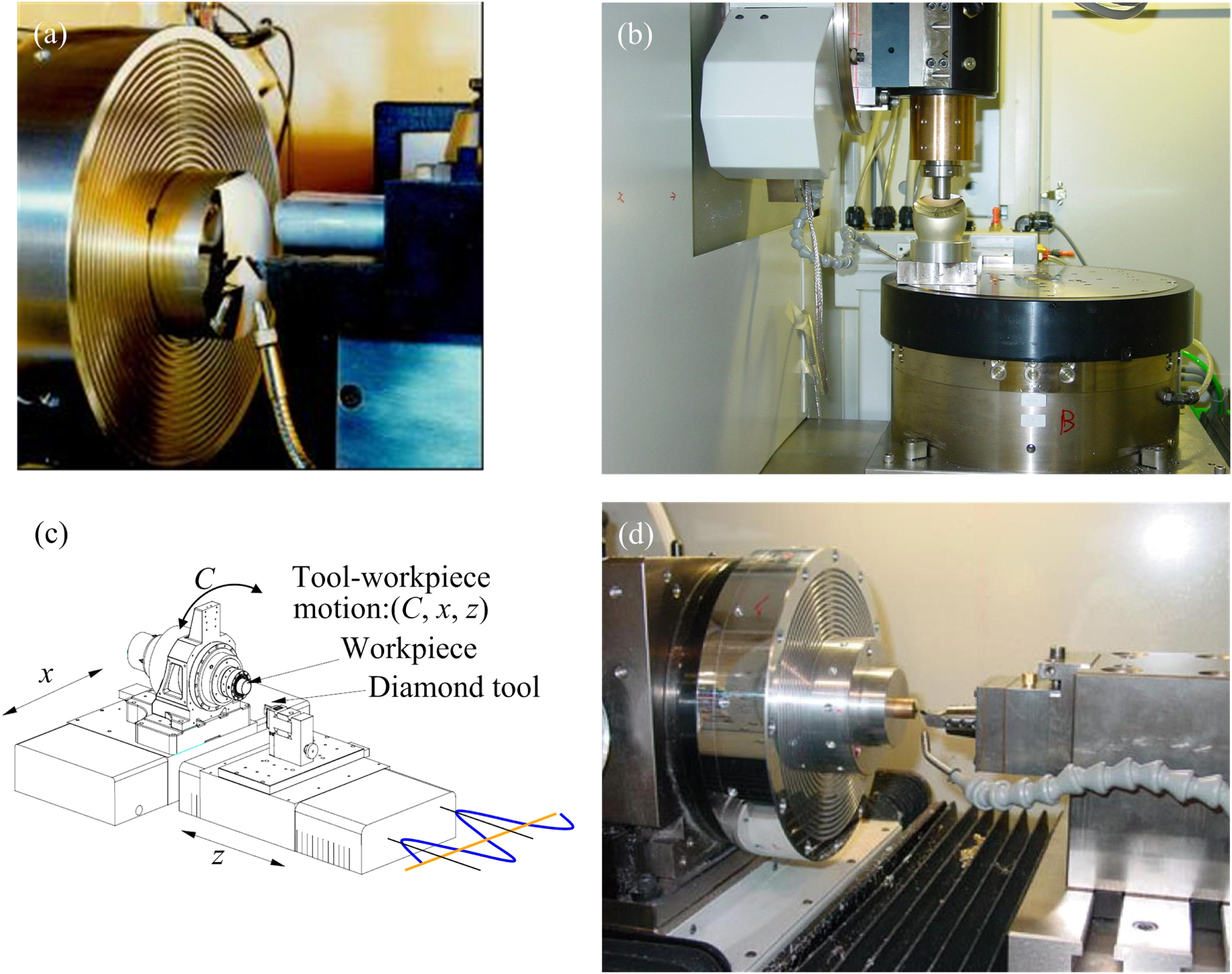
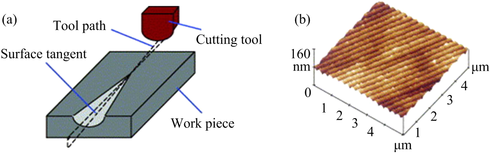
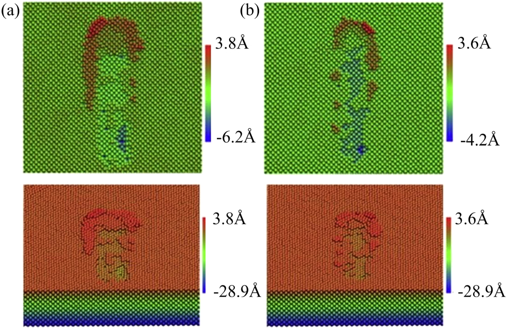
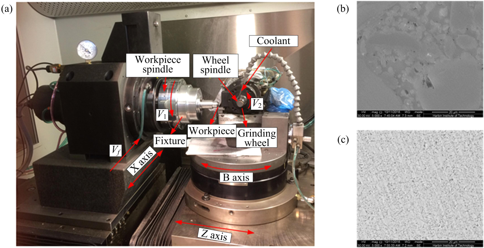
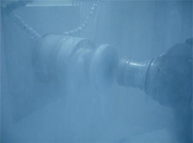
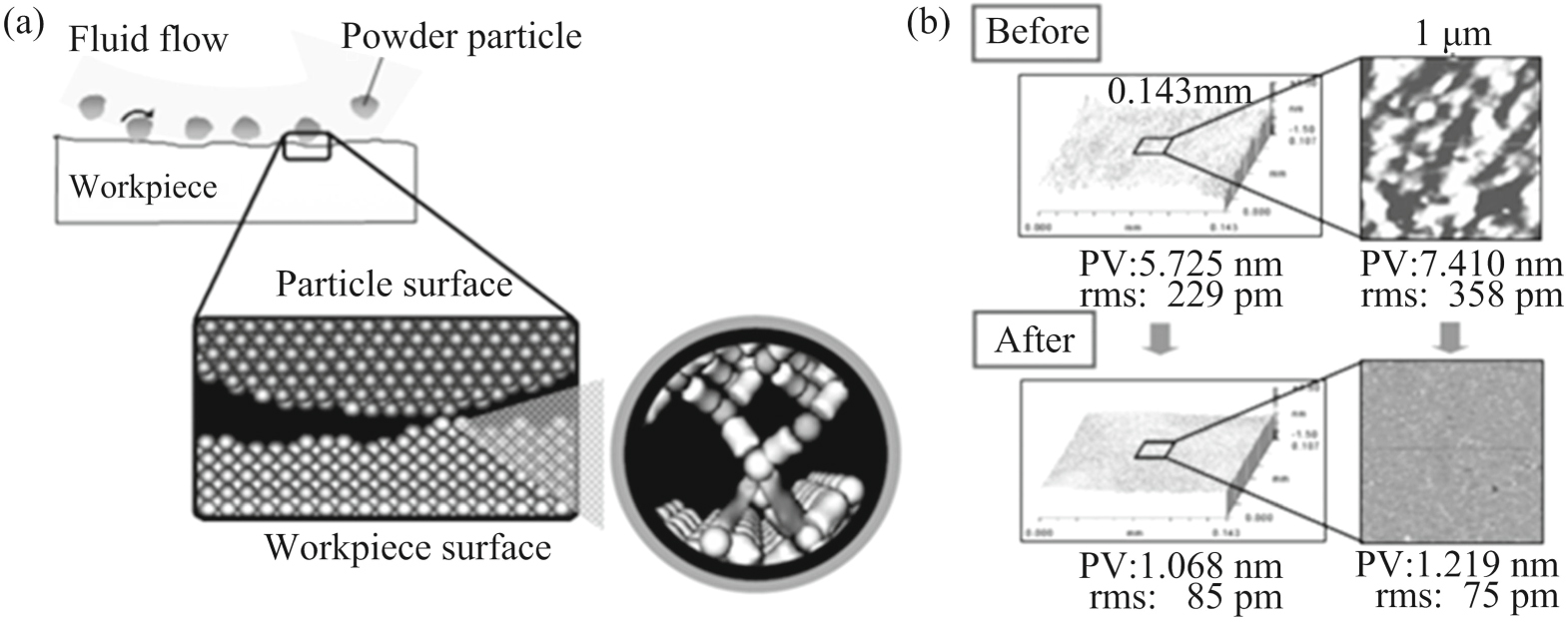
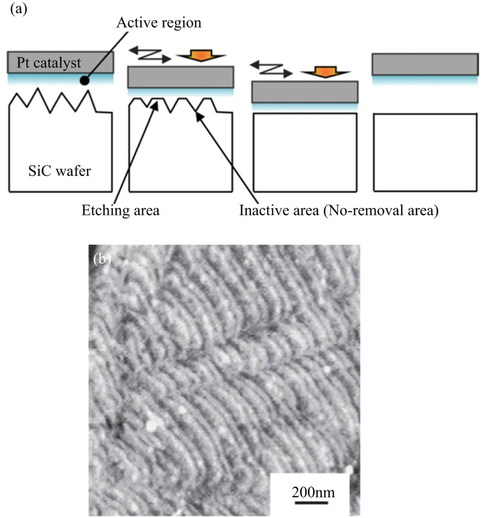
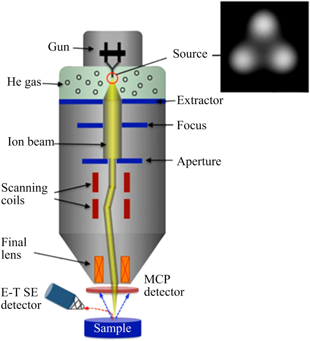
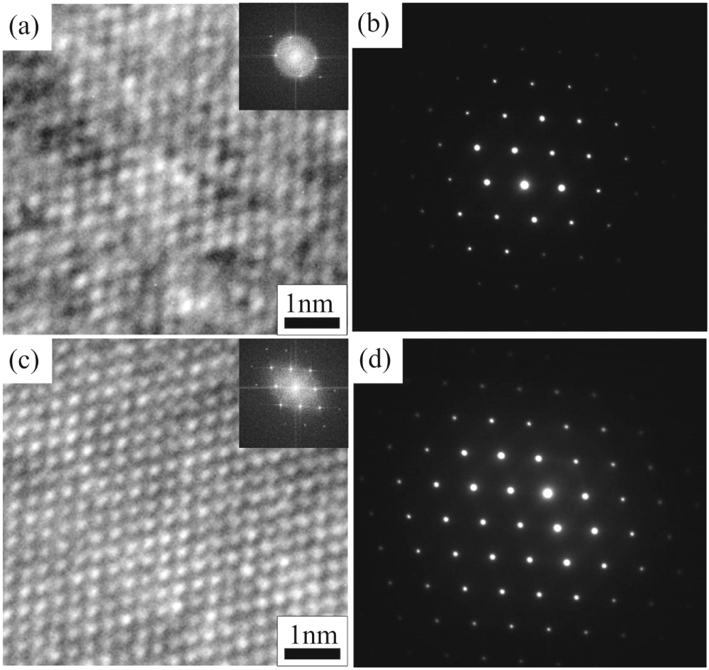
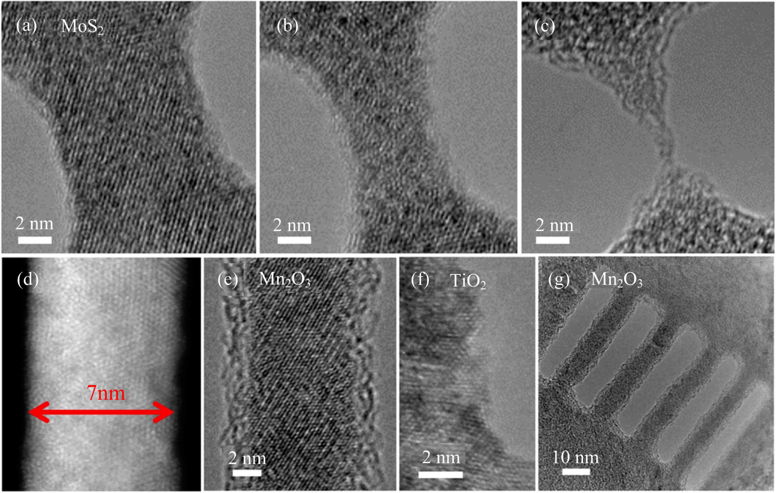
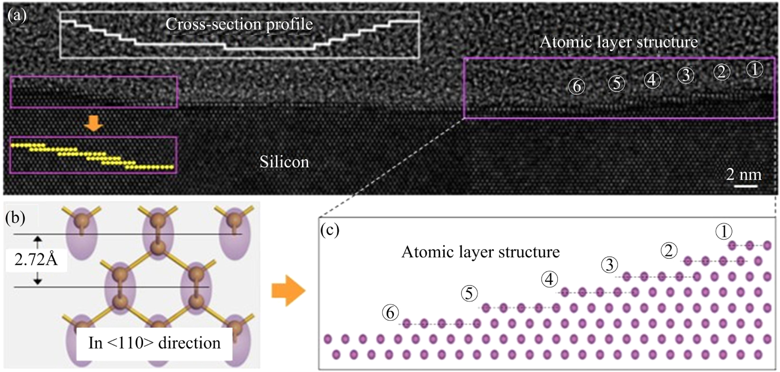
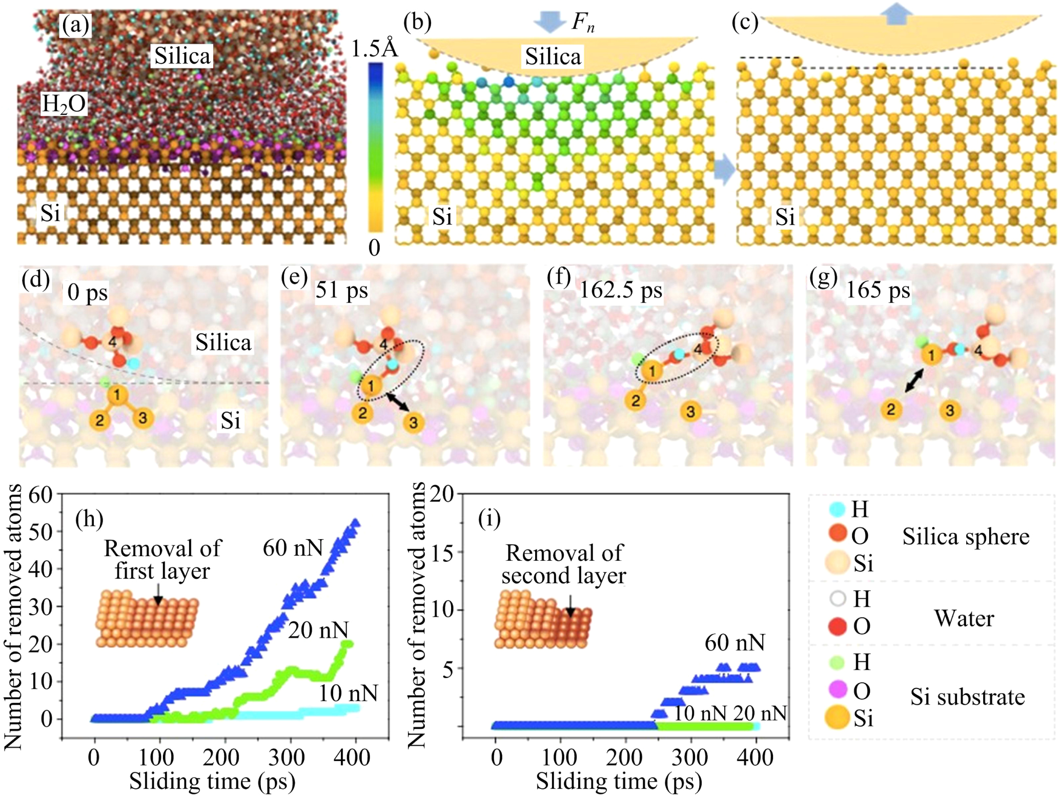
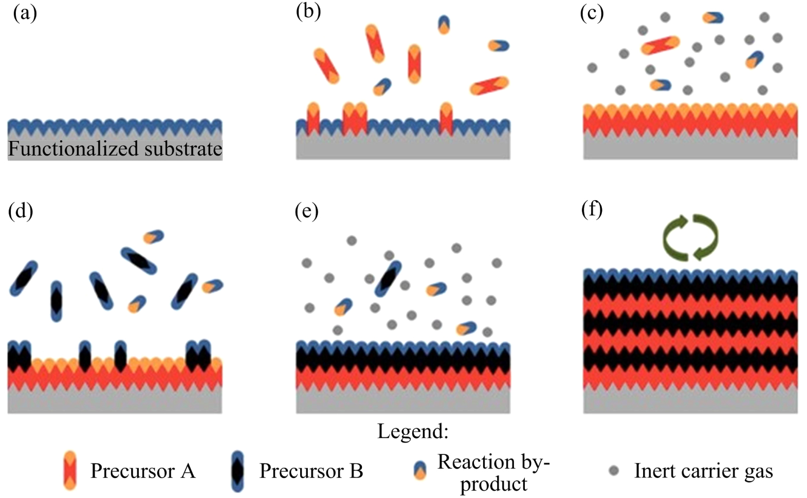
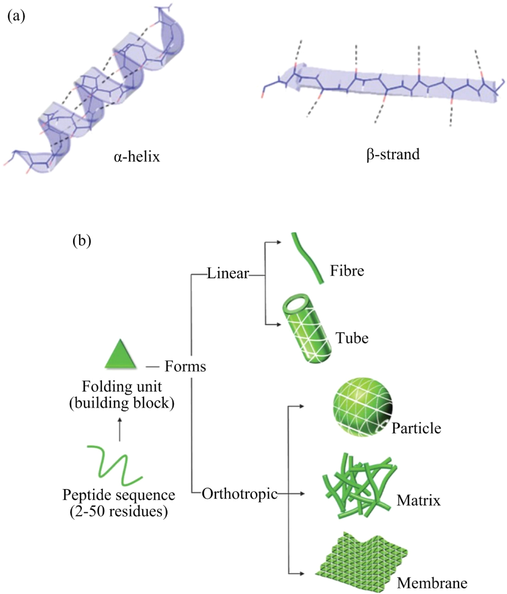
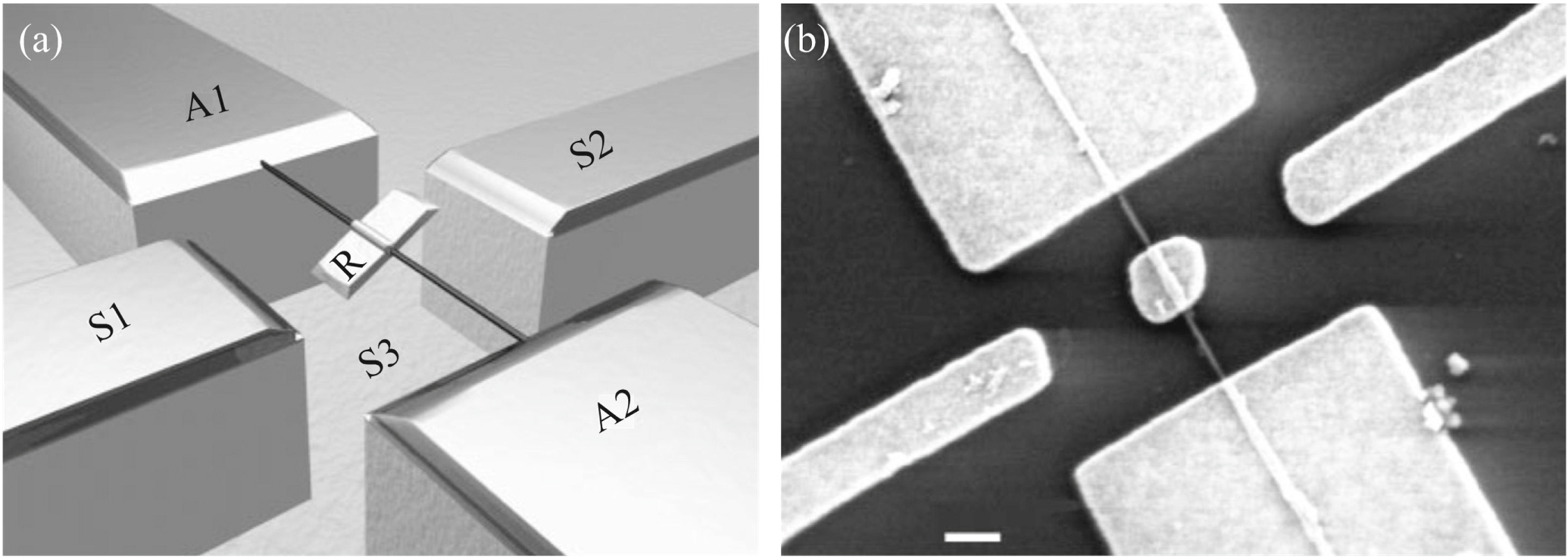
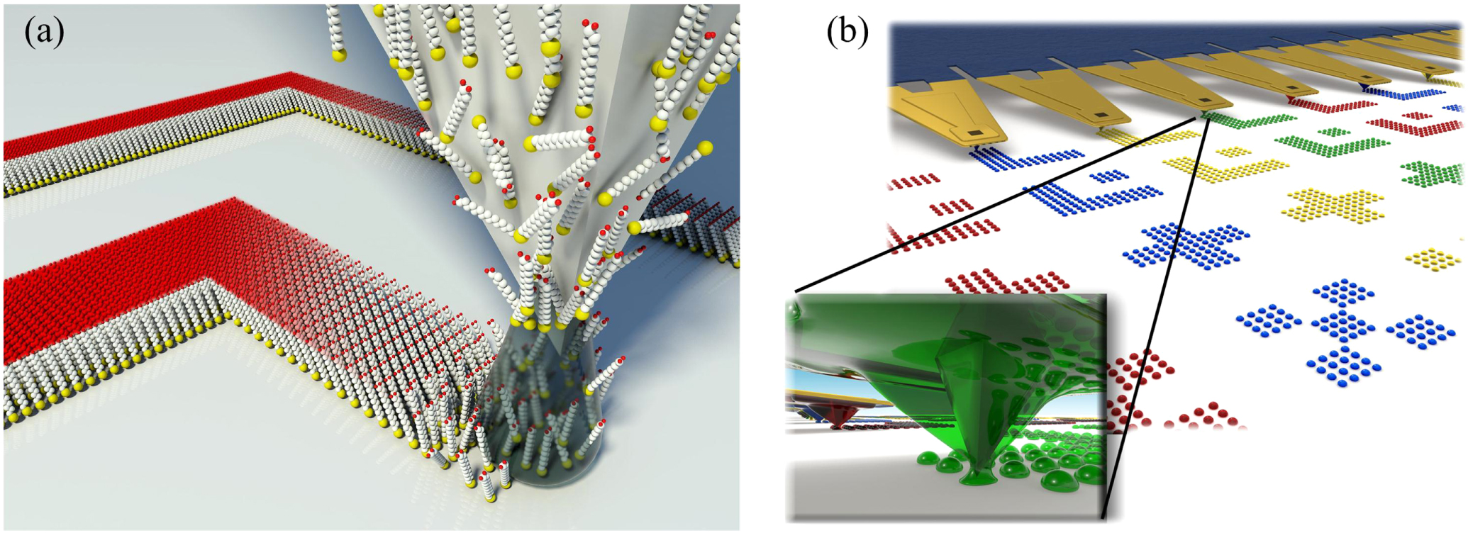
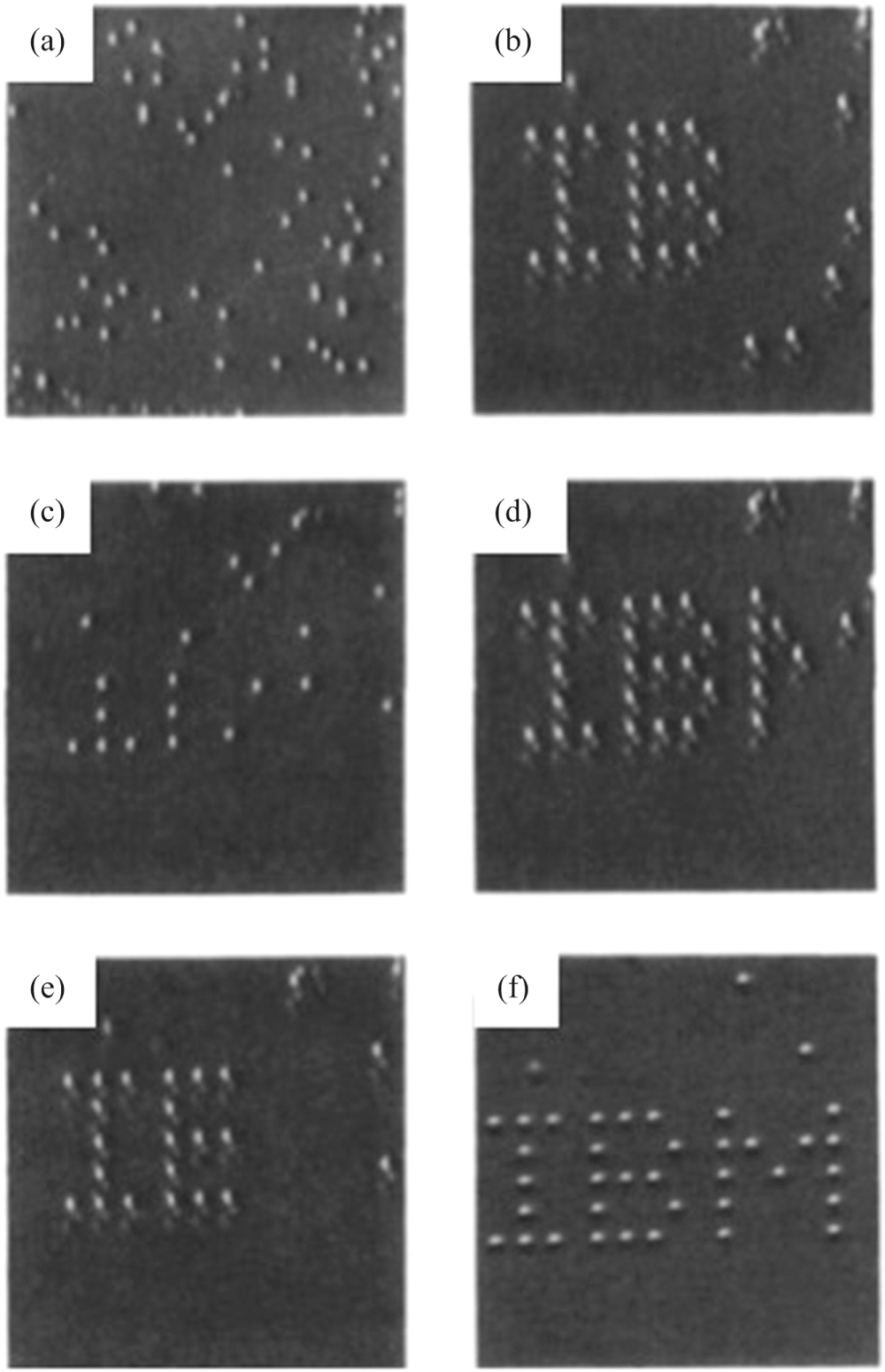
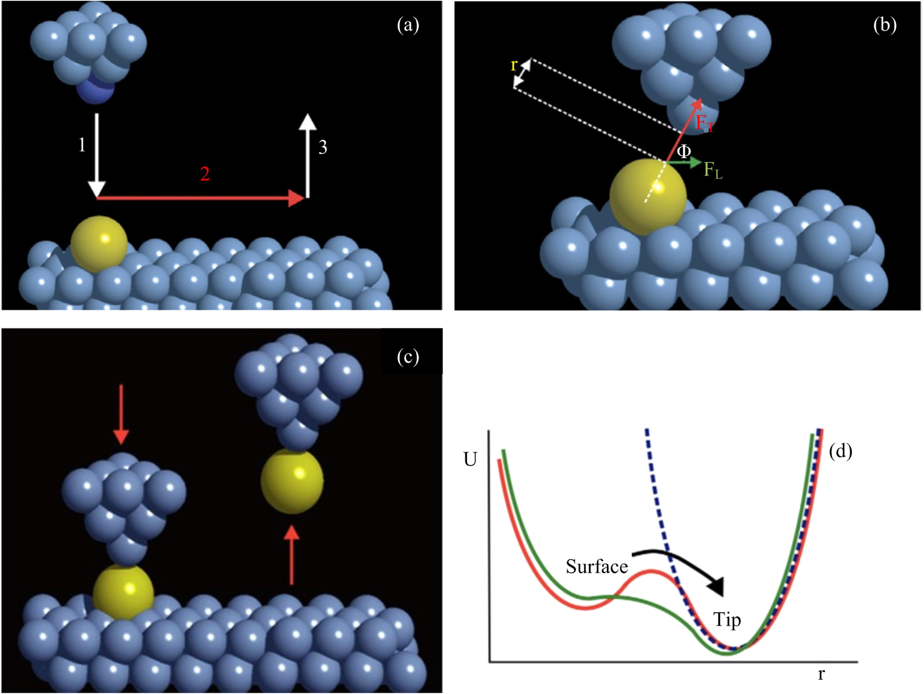
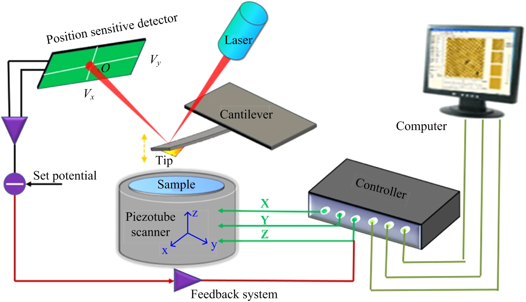
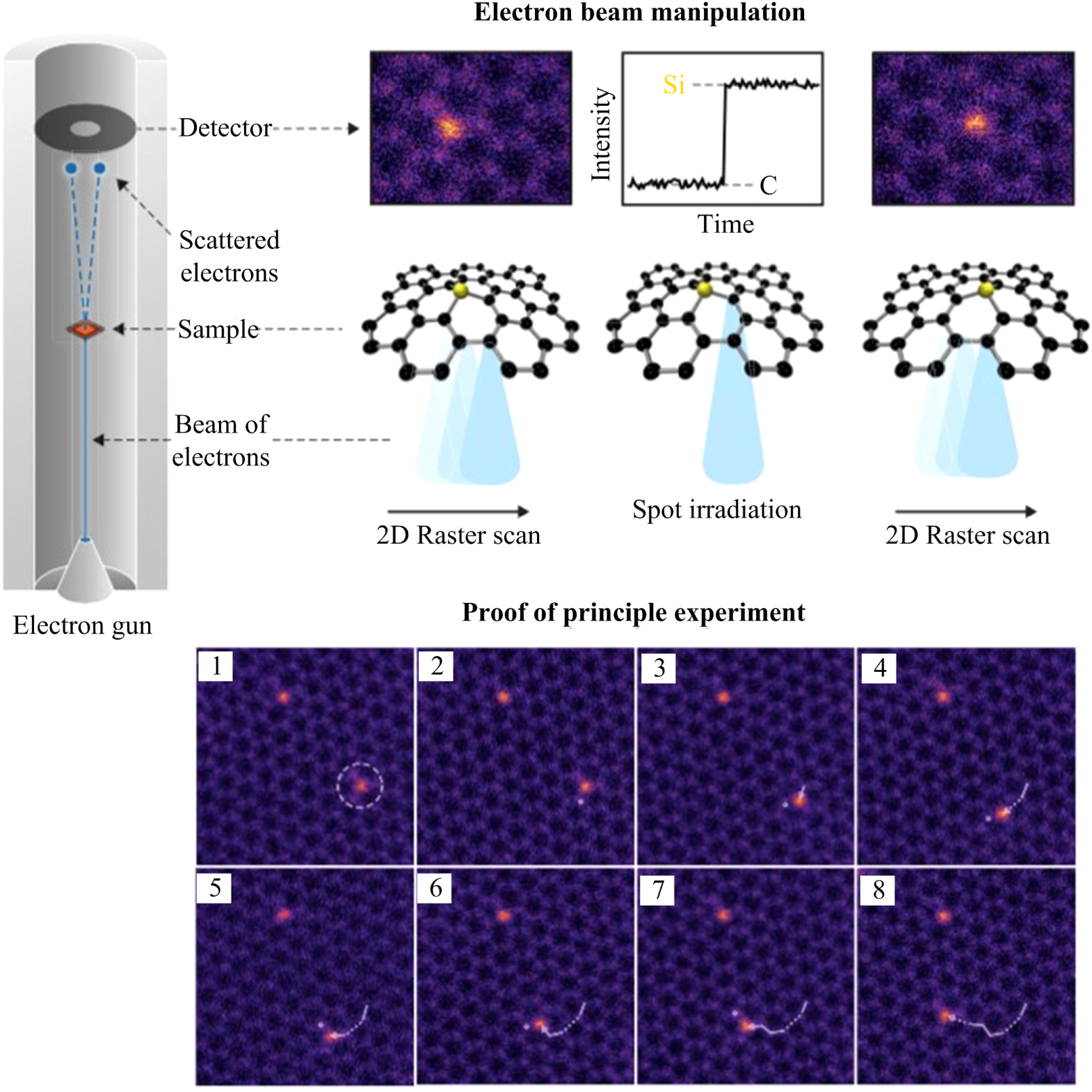
Figure 45. Theoretical strength of materials. Reproduced with permission from [129].
Download figure:
Standard image High-resolution image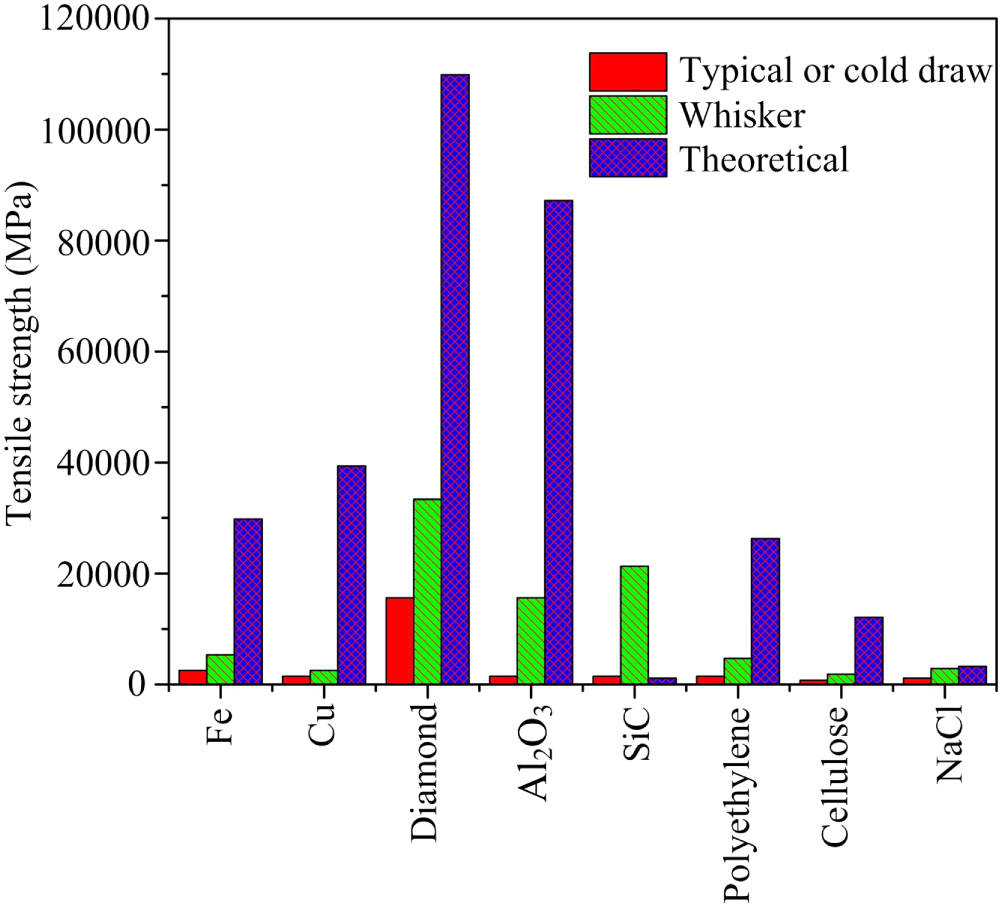
4.4. Molecular circuits
Molecular electronics, also known as moletronics, deals with the assembly of molecular electronic components using molecules as the building blocks. Molecular electronics shows potential influence in electronics and photonics with many application from conducting polymers, photochromics, organic superconductors, to electrochromics and many more [130]. Self-assembly and direct assembly are important methods for adsorbing the molecules on an electrode [131]. One of the important issues that arises is how to attach the probe electrodes to either side of a molecule. Positioning and patterning molecules selectively on a surface with molecular precision is critically important. The ideal connection requires an atomically precise interface between the two components with an optimal conductive path. Parallelization and automation are critical to integrate molecular electronic devices into an array of high reliability interfaced with microelectronic systems.
4.5. Other applications
Although ACSM is still in its infancy, it shows significant potential for applications in many fields, such as drug development, efficient solar photovatic cells, efficient high power density fuel cells, single-molecule and single-electron sensors, biomedical sensors, high density computer memory, highly selective catalysts, display and lighting systems, smart materials, etc [52]. According to a recent assessment of atomic precision manufacturing from Umbrello and Baum [132], ACSM will have a broad influence on many sectors from general material wealth, environmental issues, military affairs, surveillance, to artificial intelligence and space travel. Its positive effects could be found for material wealth, the environment, military affairs (specifically nuclear disarmament), and space travel, while negative effects were found for military affairs (specifically rogue actor violence) and artificial intelligence. The net effect for surveillance was ambiguous. They suggested that effective governance strategies should be developed to increase the benefits and reduce the harm coming from ACSM.
5. Conclusion and perspective
Since the first industrial revolution in the 1760s, human beings have experienced unprecedented development of tool precision, having shifted from millimeter level to micrometer level, single-nanometer level, and atomic level. It has been 30 years since human beings were able to manipulate a single atom using an STM. Today, the famous Moore's law is approaching its physical limit. Computer microprocessors, such as the recently announced A12 Bionic chip and Kirlin 980, use a 7 nm manufacturing process with 6.9 billion transistors in a centimeter square chip. Such limits have been pushed to a 5 nm node and even a 3 nm node [11], which represents a few tens of atoms. Human beings are already stepping into the atomic era. Meanwhile, human society is facing unprecedented global challenges from depleting natural resources, pollution, climate change, clean water, and poverty [135]. Such challenges are directly linked to the physical characteristics of our current technology base for producing energy and material products. It is the time to start changing both products and means of production. Atomic ACSM includes all of the steps necessary to convert raw materials, components, or parts into products designed to meet users' specifications. The processes involved in ACSM are not only precise at the atomic level but also remove, add, or transform the work material in atomic and/or close-to-atomic scale. Atomic and close-to-atomic scale manufacturing will provide a fundamental competence for the production of the fourth generation of core elements in contemporary industrialization.
Table 1. Comparison between AFM, STM, and STEM [101, 102, 107, 108].
| Sample material | Resolution | Advantages | Disadvantages | |
|---|---|---|---|---|
| STM (quantum tunneling) | Conductive materials | 0.1 nm lateral resolution | Ultrahigh vacuum, air, water, and other liquids and gases. | Requires very stable and clean surfaces, excellent vibration control, and sharp tips. |
| 0.01 nm depth resolution | Operate in temperatures as low as zero Kelvin up to a few hundred degrees Celsius. | Can only be used to scan samples that are not easily oxidized and conduct well. | ||
| Uses highly specialized equipment that is fragile and expensive. | ||||
| AFM (atomic interaction force) | Any materials | Lateral resolution is ∼30 nm | Generates true, high-resolution 3D surface images. | Smaller image size compared to what electron microscopes can create. |
| 0.1 nm depth resolution | Does not require special sample treatments that can result in a sample's destruction or alteration. | Slow in scanning an image, unlike an electron microscope which does it in almost real-time. | ||
| Does not require a vacuum environment in order to operate (can operate in both air and liquid). | It is not true sample topography but the interaction between the probe with the sample surface. | |||
| Could be used for organic materials. | Expensive tips. | |||
| STEM (signal generated from interaction between beam electrons and sample atoms) | Any materials | 0.05 nm | Large-area and fast scanning. | Thin section of samples. Expensive equipment. Grey images without 3D topography. |
| Multiple detectors operating simultaneously to collect the maximum possible information from each scan. |
As summarized in the above sections, human beings have already walked into the atomic world. People have developed some single-atom operation methods and are trying to develop simple devices based on these methods. Exploring the secret of macromolecular assembly in the life sciences provides a means for humans to understand the keys of life but can only manipulate a few molecules in a very simple fashion. Ultraprecision machining has pushed the limits of precision down to the sub-nanometer range, but atomic precision machining systems capable of generating complex atomic structures still do not exist.
What shall we do in the future?
- Explore nature in terms of ACSM: Atomic and close-to-atomic scale manufacturing processes are still quite limited to single atom manipulation and macromolecular assembly; and the fundamental mechanisms of these processes need to be explored. Additionally, more ACSM processes should be explored and developed, such as a recent work on building a molecule from two atoms using optical tweezers [133].
- Functional devices: It has been 30 years since the invention of STM. However, the number of functional devices developed is still quite limited, although we have witnessed the conception and demonstration of the single-atom transistor [93] or single-electron transistor [134]. More applied devices need to be developed based on ACSM processes.
- Extensive materials: Existing ACSM processes can only manipulate a limited number of materials with limited capability, such as STM to manipulate weakly bonded atoms. Such limitations can also be found in AFM and STEM manipulation. Macromolecular assembly is limited to DNA, proteins, and peptides; and their interfacing mechanism is still not clear. There is still a large amount of materials out of reach. We are still far away from developing atomically perfect materials.
- High throughput: As a manufacturing process, the final goal is that ACSM will be used to convert raw materials, components, or parts into products designed to meet users' specifications. As a result, high throughput via parallelization and automation is critically important. This means atomic manipulation needs to be connected to mass production using machinery. It will be one of the most important steps to developing atomically precise machine tools to converge atomic precision with atomic-scale manufacturing. In addition, atomically flat surfaces without dangling bonds and other defects are also important for the fabrication of atomic-level devices [135].
Atomic and close-to-atomic scale manufacturing is still in its infancy. The discovery of atomic devices, novel materials, and life sciences will lead to new opportunities to apply ACSM to meet the challenges faced by human beings. As a representative of the next generation manufacturing technology, startup, planning, and implementation will play a positive role in supporting the next phase of manufacturing development, i.e. Manufacturing III.
Acknowledgments
The authors gratefully acknowledge the support from the National Science Foundation of China (Grant Nos. 51320105009, 61635008, and 61675149) and the Science Foundation Ireland (SFI) (Grant Nos. 15/RP/B3208 and 18/FIP/3555).