
Abstract
Additive manufacturing (AM) technology is considered one of the most promising manufacturing technologies in the aerospace and defense industries. However, AM components are known to have various internal defects, such as powder agglomeration, balling, porosity, internal cracks and thermal/internal stress, which can significantly affect the quality, mechanical properties and safety of final parts. Therefore, defect inspection methods are important for reducing manufactured defects and improving the surface quality and mechanical properties of AM components. This paper describes defect inspection technologies and their applications in AM processes. The architecture of defects in AM processes is reviewed. Traditional defect detection technology and the surface defect detection methods based on deep learning are summarized, and future aspects are suggested.
Export citation and abstract BibTeX RIS

Original content from this work may be used under the terms of the Creative Commons Attribution 3.0 license. Any further distribution of this work must maintain attribution to the author(s) and the title of the work, journal citation and DOI.
1. Introduction
At the start of the development of additive manufacturing (AM) technology in the 1990s (AM was called 'rapid prototyping technology' at that time), researchers attempted to prepare non-metallic parts based on various rapid prototyping manufacturing methods [1–3]. Following this, the preparation of metal parts was realized through subsequent processes [2]. Compared with traditional metal manufacturing technologies such as forging machining, forging, and welding, AM technology has advantages such as no need for tools or molds, high material utilization, short product manufacturing cycle, and the ability to manufacture complex structures [1]. All AM systems work on the same principal of building a structure additively from a substrate. Each method has advantages and disadvantages [4]. According to the ASTM standard, the AM processes can be divided into seven categories: Binder Jetting, Material Extrusion, VAT Photo-polymerization, Material Jetting, Sheet Lamination, Directed Energy Deposition (DED), and powder bed fusion (PBF) [5]. These AM processes have the ability to print various materials including polymers, metals, ceramics, and composites. Table 1 summarizes the commercial names and principal operations of AM processes [6].
Table 1. AM process categories [6].
| AM technology | Types | Description |
|---|---|---|
| Material extrusion | FDM | Material is extruded through a heated nozzle |
| Vat photopolymerization | Stereolithography apparatus (SLA), digital light processing (DLP) and continuous liquid interface production (CLIP) | Selective curing of liquid photopolymer using light activated polymerization |
| Powder bed fusion | Selective laser sintering (SLS), SLM, direct metal laser-sintering (DMLS), electron beam melting (EBM), selective hot sintering (SHS) and laser beam melting (LBM) | Selective thermal fusion of powder using a laser or an electron beam |
| Binder jetting | Three-dimension printing (3DP), binder jetting (BJ) and powder bed and inkjet head (PBIH) | Deposition of liquid bonding droplets to a powder bed using an inkjet print head |
| Material jetting | Material jetting (MJ) and drop on demand (DOD) | Deposition of material droplets by an inkjet print head |
| Sheet lamination | Laminated object manufacturing (LOM) | An AM process in which sheets of material are bonded to form a part |
| Directed energy deposition | Laser metal deposition (LMD), electron beam freeform fabrication (EBF), laser engineered net shaping (LENS), directed laser deposition (DLD) and direct metal deposition (DMD) | Wire or powder is extruded or blown from a nozzle and melted by an electron beam or a laser |
Metal products can be printed by binder jetting, sheet lamination, PBF, and DED. These processes are not limited to metals [7]. Metal AM technology differs from traditional machining and other manufacturing technologies that remove materials step by step. AM is based on the principle of discrete accumulation, using alloy powder or wire as raw materials and high-energy beams, such as lasers or electron beams, for in-situ metallurgical melting [8]. The goal of the manufacturing industry is to produce functional parts that meet industrial requirements [9]. AM is especially suitable for low-cost, short-cycle, rapid prototyping of large and complex metal structures for aerospace and defense equipment, such as spacecraft, missiles and satellites [10–13]. In the PBF processes, the melted material rapidly solidifies, resulting in a stack of bound layers that constitute the final part. When the feed material is deposited onto the substrate, it is fused following a given pattern. Near-net-shape manufacturing of high-performance metal parts is completed directly from the digital model of the part [14].
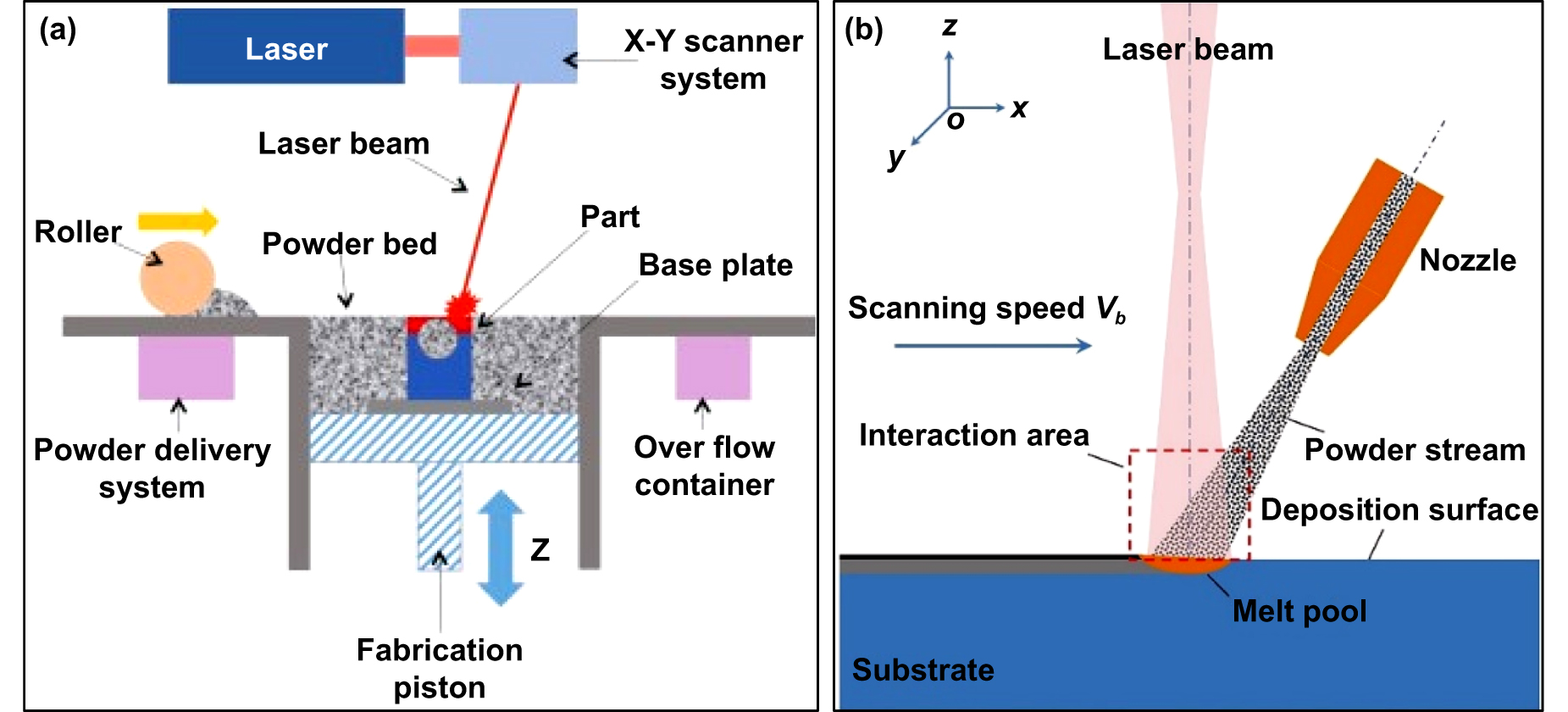
As shown in figure 1(a), the PBF system employs a powder deposition methodology, spreading powder on the substrate layer by layer. Once the powder is distributed, the PBF system utilizes energy from an electron beam or laser to sinter the powder following a cross-sectional pattern defined by a digital 3D model of the part. After a layer is completed, the building platform is lowered, and the manufacturing operation is carried out continuously [15]. DED is a metal-based AM process that can create 3D parts by melting materials during the deposition process. This process consists of two categories according to the material delivery mechanism: powder feeding and wire feeding. As represented in figure 1(b), the DED system does not melt powder that is already spread on the manufacturing platform. Instead, the material deposition and melting processes occur simultaneously, where a cladding nozzle delivers powder to the focus of a high-power laser beam that concurrently melts it [16].

Download figure:
Standard image High-resolution imageAt present, AM alone is not capable of producing parts with acceptable mechanical properties and surface roughness that meet the requirements of most applications [17, 18]. Insufficient knowledge of the process dynamics significantly affects the application of additively manufactured parts. For example, the metallurgy and thermophysical phenomena that occur within selective laser melting (SLM), a widely used process, are still not fully understood. More specifically, the interactions between the laser beam and powder and the molten pool and powder bed and the melting process are very complicated. In the SLM processes, the phenomenon of rapid solidification under the ultra-high temperature gradient and the strong bonding forces in the manufactured area need in-depth assessment. In addition, the evolution of a component's internal structure and the thermal stresses that occur under cycling conditions require more exploration. During printing operation, various internal defects, such as powder agglomeration, balling, porosity, cracks, powder volatilization, and thermal stresses, occur between different powder layers and within individual layers, which significantly affects the internal microstructure, mechanical properties, and quality of the final part [19–24]. Although AM technology has been relatively successful at attaining sufficient mechanical properties, defects and geometric inaccuracy still limit component adoption in the industry. Defects often occur in built components due to discontinuities in the printing process and other extraneous factors [25, 26]. As a result, defect detection technologies have been widely used in AM processes. These technologies detect defects such as surface spots, pits, holes, scratches, chromatic aberrations, and the internal structure of the tested sample [27–29]. Eventually, relevant information is obtained, such as the depth, size, contour, and the category of the surface or internal defect [30].
Detection technology must meet the following requirements for metal AM technology: low cost, rapid detection, adaptation to complex geometric structures and poor surface quality, and detection of multiple types of defects [31]. Methods of detecting metal AM can be divided into traditional non-destructive defect detection technology and defect detection technology based on machine learning. The first type of detection technology, the monitoring of materials in the AM process, focuses on abnormal phenomena of materials by detecting the characteristic quantities. This detection method has a certain predictive effect on the occurrence of defects [32]. Timely detection of defects in the AM process can help adjust the manufacturing process and take certain measures to remove the defects or stop manufacturing directly to reduce material and time loss [33]. Following the advancement timeline of defect detection technologies, non-destructive techniques evolved from infrared imaging defect detection, penetrant testing, and eddy current testing to ultrasonic inspection and x-ray testing [34]. In addition to traditional ultrasonic testing methods, many scholars have conducted research on laser ultrasonic testing methods [35]. The advantage of non-destructive techniques is that the test results reflect the final quality of the parts, which ensures the reliability of the parts during use. Post-testing can also establish the relationship between process conditions and part quality [36, 37]. Recently, machine learning defect detection has emerged as a technology that uses advanced equipment and deep learning methods to conduct in-process imaging for defect identification [38]. Machine learning detection for AM is still in its infancy [39–41].
This study aims to summarize different categories of defects and defect inspection technologies in AM processes by introducing various widely applied defect detection methodologies. Some defects that appear in general AM processes are also presented. Section 2 illustrates a detailed description of defects. Section 3 summarizes different traditional defect inspection technologies. Section 4 discusses machine learning defect detection technologies. Section 5 presents the latest research of defect detection technologies. Section 6 proposes the future prospects of defect detection technology. Finally, section 7 presents the authors' conclusions.
2. Categories of defects
The large number of input manufacturing parameters in AM technology processes optimize product quality, thereby reducing observed material discontinuities. Despite the enormous benefits of AM, various defects limit the process in terms of precision, repeatability, and resulting mechanical properties. Although, in some cases post-processing techniques can reduce or eliminate defects in AM processed parts. Improving the processing quality of parts is important to meet challenging industrial requirements. Understanding defects and their causes represents the first step to inspect and reduce them. Most of the defects, such as cracking, residual stresses, porosity and balling, have been researched and discussed. The categories of defect causes include equipment, manufacturing processes, build preparation choices, and powder. Equipment-induced defects are caused by improper setting and calibration of the main system components. Manufacturing process-induced defects are connected to the interaction between the powder, the beam and the previous layer [13].
2.1. Cracking
Internal cracks are common defects that appear in AM components and mainly result from thermal stresses. These defects significantly impact part performance and restrict the application of AM products [42–45]. Therefore, the occurrence of cracks must be controlled. Many researchers have conducted research on the formation mechanism of cracks, its influencing factors, and treatment methods to reduce and eliminate cracks from the AM process. Studies have shown that the cracks typically generate when continuous and semi-continuous liquid films form on the grain boundaries of the heat-affected zone and when tensile stresses form within parts [46–49]. AM process parameters are the main factors that affect the occurrence of cracks in components. Additionally, the direction of the grains determines the growth direction of the crack [49]. During the manufacturing process, once a crack has occurred, it spreads along the molten layer, significantly affecting the mechanical properties of the component, and even risking its disposal [50, 51].
The cracking phenomenon is presented in [52], as shown in figure 2. The results show that significant cracking occured between Inconel 738 layers and a directionally solidified (DS) substrate when the AM process energy was high enough to cause over-melting on the substrate surface. The cracks originated from and expanded along the grain boundaries of the DS superalloy matrix, spreading throughout the deposited layer and the entire interface.
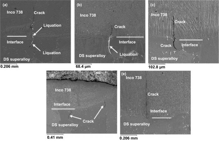
Figure 2. The cracking phenomenon in selective laser melted parts: (a) apparent liquation cracking in the DS substrate and liquation penetration into the Inconel 738 deposition layer; (b) liquation cracking in the DS substrate but crack penetration into the Inconel 738 deposition layer without liquation; (c) cracking in the DS substrate and crack penetration into the Inconel 738 without liquation; (d) cracking in the DS substrate without liquation and no crack penetration into the Inconel 738 deposition layer; (e) no cracking in the DS substrate but crack originates in the interface and propagates into the Inconel 738 deposition layer [52].
Download figure:
Standard image High-resolution image2.2. Residual stresses
In AM processes, the temperature of the metal powder varies considerably and thermal stresses easily form within the component, causing significant uncertainty with regards to the quality of the final part. When the stresses trapped inside the component are suddenly released, cracks emerge on the surface, affecting the performance and life of the component. Residual stresses in SLM have been associated with two different mechanisms, including the cool-down phase of molten top layers and the thermallayers and the thermal gradient mechanis gradient mechanism [53]. Thermal stresses induced by powder melting are particularly significant during the SLM process. Thermal stresses cause warpage and cracking and ultimately deform the component [54]. A schematic diagram of residual stress formation during AM processes is shown in figure 3. Figure 3(a) shows the accumulation of residual stress in the first layer of a metal sample during cooling and solidification. The force balance produces compression at the center, while the surface tension produces the maximum stress. After the first layer solidifies, the second layer of powder is added and immediately melted by the laser beam. As shown in figure 3(a), the bottom of the first layer contains stress, while the top part is exposed to the heat of the melted layer. The heated top part expands, but it is limited by the cold bottom part of the first layer. As shown in figure 3(b), mixed mechanisms form residual stresses in the fabricated metal components [55].

Figure 3. Residual stress formation during AM process of metallic parts: (a) first layer and (b) second layer [55].
Download figure:
Standard image High-resolution imageRelevant studies have found that the most influential factors in the development of residual stresses are material properties, component height, powder layer thickness, scanning strategy, and related process parameters [53, 56]. Obviously, the control and elimination of residual stresses in components is a key factor in determining the quality of AM products [53]. In recent years, researchers have considered reducing and eliminating residual stresses through selecting appropriate process parameters to curb the formation of cracks [57] and other control methods.
2.3. Porosity
Porosity is a common phenomenon in both PBF and DED processes. Pores originate from a lack of fusion and trapped gas, which directly affects the density and mechanical properties of finished components and determines their performance [58–60]. Generally, components with higher performance requirements also have higher porosity requirements. However, there are components that are required to achieve a certain degree of porosity for specific applications. Some researchers have studied the porosity of PBF manufactured components, paying attention to the control of porosity. When the demand for functional parts is high, component density requirements are also high. Therefore, it is necessary to adopt effective methods and processes that reduce pores. To achieve that, understanding the formation mechanism of pores is critical [61]. Pores form when a material undergoes rapid melting and solidification during PBF processes, which entraps gases in the molten pool and prevents their timely release. Pores are generally small and spherical in shape. Pores are not only process-induced, but may exist even before the melting process, especially if the feed material was prepared using atomization, where the preparation environment is argon purged, inevitably leaving traces on the solidified powder particles. On this basis, gas forms in metal powder due to the melting process or as a byproduct of powder production. If these gases are not released on time, pores can form in the component [62, 63]. Günther et al studied the impact of two different AM routes, i.e. EBM and SLM on the fatigue life of the titanium alloy Ti–6Al–4V in the high cycle fatigue and very high cycle fatigue regimes [64]. As shown in figure 4, the fracture surfaces of the failed specimens of batches SLM-1b, SLM-2, and EBM were investigated by SEM.
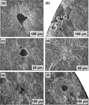
Figure 4. Different representative defect types in SLM-1b, SLM-2, and EBM batches: (a)–(c) batches of SLM-1b, (d) batches of SLM-2, and (e), (f) batches of EBM [64].
Download figure:
Standard image High-resolution imageZhang et al carefully studied the relationships between surface pore defects and bubbles originating on the melt pool surface in DED processes using high-speed photography at up to 20 000 frames per second [65]. Gas-atomized powder (nominal composition of Ni–8Cr–6Al–6Co–5W in wt.%) with a particle size of 50 ± 10 μm was supplied at a feeding rate of 15.5 g min−1. Figures 5(a) and (b) show the sporadic occurrence of several macroscopic, surface-opening pores along the track edges. These spherical pores seemed to be linearly distributed along the laser scanning direction, with a diameter of 300–400 μm.
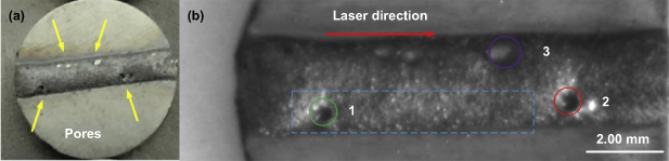
Figure 5. Morphology of a single-track. (a) Top view showing the pore defects (yellow arrows) distribution along the track edges. The laser source was scanned from left to right. (b) Three surface pores (1–3) are indicated by circles [65].
Download figure:
Standard image High-resolution image2.4. Balling
Melt ball formation, a.k.a. balling, occurs when molten material solidifies into spheres instead of solid layers, which is a severe impediment to interlayer connection [50]. Generally, balling formation occurs when spherical particles are produced in the component due to interactions between the molten pool and the metal powder. This happens under the influence of the manufacturing environment and prevents the full melting of some powder particles that mix within the component [66–69]. Metal balls form independently and are easily generated in the layer-by-layer scanning process, resulting in a rough, bead-shaped surface that produces irregular layer deposition that adversely affects the density and quality of the part [13]. In addition, balling also affects the normal operation of the powder spreading roller, and in severe cases can hinder the spreading mechanism [12]. Balling can increase the surface roughness of the component and reduce its density and mechanical properties. Therefore, it is necessary to explore and study the suppression and elimination of the balling problem in PBF manufactured components and possible treatment methods.
Qiu et al performed SLM of alumina with pressure assistance on the powder bed. They investigated defects such as balling [70]. They used three types of commercial alumina powders (purity of 99.5 wt%, provided by Henan Jiyuan Brother Material, China) with different particle size distributions. Figure 6 shows optical images of the balling phenomenon under different laser energy densities. The balling diameter increases as the laser energy density increases, which indicates that the particle size has no significant influence on the microbead diameter. The balling phenomenon influences the geometric accuracy of the component and increases porosity and affects mechanical properties.
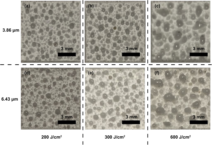
Figure 6. The balling phenomenon under different hatch spaces and different particle sizes: (a) 0.15 mm, (b) 0.10 mm, (c) 0.05 mm, (d) 0.15 mm, (d) 0.10 mm, and (e) 0.05 mm [70].
Download figure:
Standard image High-resolution imageIn recent years, defect detection technology has been widely used in various industrial scenarios. Defect detection technology refers to the detection of defects, such as surface spots, holes, scratches, and the internal structure of the tested sample; it also obtains relevant information such as the depth, size, contour, and the category of the defect on the surface or inside of the tested sample [71–74]. According to the development process of defect detection technology, it can be divided into traditional defect detection technology and machine learning defect detection technology based on deep learning that has emerged in recent years, which uses machine vision equipment to obtain images and identify whether defects are present in the collected images. The following sections summarize traditional defect detection techniques and surface defect detection methods based on deep learning in recent years, and further subdivides and classifies various typical methods and compares them.
3. Traditional non-destructive defect detection technology
Traditional non-destructive defect detection methods include infrared imaging defect detection, penetration defect detection, eddy current defect detection, and ultrasonic defect detection.
3.1. Infrared imaging defect detection
The principle of infrared thermal imaging technology displays the shape and contour of defects through the thermal radiation intensity of the additively manufactured workpiece. The thermal radiation difference between the defects and the surrounding materials makes the defects stand out in infrared images. According to the theoretical results of the thermoelastic effect in the isotropic homogeneous body, metal samples with different defects have different material properties. Defects will affect the heat conduction in the metal samples, and then affect the temperature field in the samples. Using a certain method to input heat into the samples can detect the temperature field of the samples through various infrared sensors to obtain defect information. Using this conclusion, it is possible to use infrared thermal imaging cameras to detect the surface temperature field of additively manufactured objects, find areas with abnormal temperatures, and determine the location of defects. Schwerdtfeger et al [75] performed infrared photography on each layer in the electron beam selective melting process. They identified the position of the defect based its the radiation intensity, and obtained cross-section verification test results through grinding. The test proves that the infrared image corresponds with the actual defects in the part, and the radiation intensity at the defect is higher. Bartlett et al [76] used a long-wave infrared camera to photograph each layer during the manufacturing process. They regarded areas where the average temperature between the layers differed by more than 1% as defect areas. The defects were detected in real time during the manufacturing process. The test showed that this method detects 82% of unfused defects and all unfused defects larger than 500 μm. However, this method can only detect 33% of of micro-hole defects.
3.2. Penetration defect detection
Penetration defect detection is a non-destructive testing method that uses capillary phenomena to inspect the surface defects of materials. Its working principle is simple: A penetrant containing fluorescent or colored dyes is applied to the surface of the workpiece. Under capillary action, the penetrant infiltrates and settles into surface defects. Any excess penetrant on the surface of the workpiece is removed after drying. A developer is then applied on the surface of the workpiece and reacts with the penetrant under the effect of a light source, which displays the trace of the penetrant and the defects. Penetrants containing fluorescent agents are significantly more sensitive for defect detection than ordinary penetrants. The factors that affect the sensitivity of penetrant detection include imaging reagents, penetrant performance, and the effects of defects themselves [77].
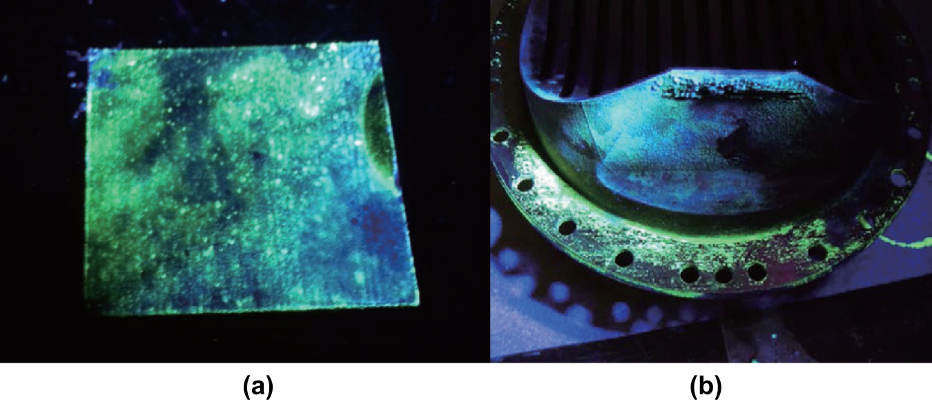
Fluorescent penetrant detection technology is easily affected by the structure of additively manufactured workpieces, and it is highly sensitive to surface-opening defects and intuitive results. Penetration testing methods are not suitable for testing porous or rough additively manufactured parts that have not undergone post-processing or polishing. The Glenn Research Center of NASA uses the penetration method to inspect the surface of key components of liquid propellant rocket engines manufactured by SLM and EBM processes. The Marshall Space Flight Center uses the penetration method to inspect the POGO-Z baffle. As shown in figure 7, the highlighted parts are defects caused by the rough surface of the additively manufactured parts [78].

Figure 7. Results of PT of AM structures for aerospace: (a) sample of rocket gas injector and (b) POGO–Z bezel [78].
Download figure:
Standard image High-resolution imageThe fluorescent penetrant detection method can detect tiny cracks in surface openings. Therefore, a fluorescent penetrant is a suitable non-destructive method for inspecting the surface defects of non-porous additively manufactured structures.
3.3. Eddy current defect detection
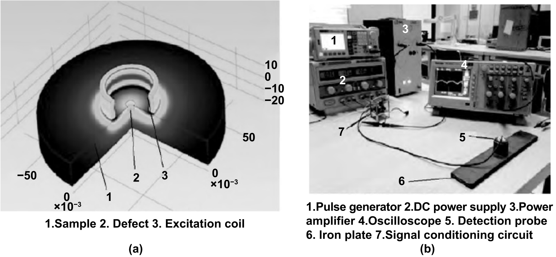
Eddy current testing is a non-destructive testing method that uses the principle of electromagnetic induction to identify defects in conductive materials by measuring the changes in induced eddy currents. Exciting a coil applies an alternating magnetic field to the test piece and generates an eddy current under the action of the alternating magnetic field. The current in the coil changes due to the eddy current reaction. The eddy current change can be measured, thereby obtaining the status information of the test piece defect. The eddy current distribution and size are determined by factors such as the shape and size of the coil, the AC frequency, conductivity, permeability; the shape and size of the test piece, the distance between the test piece and the probe, and the surface defects of the test piece [79]. Therefore, the detected eddy current conveys information about the material, defect, shape, and size of the test piece. The main factors that affect the accuracy of eddy current detection include the type and parameters of the coil and the material and contour of the detection part.
Eddy current testing technology can be used in harsh environments. It meets some of the requirements of AM for non-destructive testing and is suitable for detecting defects such as cracks and non-fusion pores. Du et al [80] studied eddy current detection technology on defects of composite machining parts. They milled the plane after the each layer was deposited and used the eddy current method after removing the interference of surface roughness. In order to verify this principle, they established a corresponding finite element model based on ANSYS and studied the influence of factors such as excitation frequency, temperature, and lift-off height on the inspection results. They used x-ray inspection technology to verify the measurement results. The inspection results of Ti-6Al-4V strips with unfused defects obtained by the direct laser deposition process are shown in figure 8. It can be seen from figure 8 that this method can effectively detect defects in parts.

Figure 8. Eddy current detection results [80].
Download figure:
Standard image High-resolution imageAlthough eddy current detection technology can be used in harsh environments, such as high temperatures, temperature has a greater impact on the electromagnetic properties of materials. Additively manufactured parts often have complex temperature fields, so it is still difficult to accurately detect part defects through eddy current. In the future, we can develop corresponding signal processing methods by designing a reasonable probe form to overcome the interference of temperature and surface roughness on the detection results.
3.4. Ultrasonic defect detection
Ultrasonic testing refers to a non-destructive testing method that uses ultrasonic waves to inspect the internal defects of metal components. It uses a transmitting probe that emits ultrasonic waves to the surface of a component through a couplant. When the ultrasonic waves propagate inside the component, they emit different reflected signals as they encounter different interfaces. The defects inside the component can be identified based on the time difference between the transmission of different reflected signals to the probe. The height and position of the echo signal displayed on the phosphor screen reveal the size, position, and general nature of the defect. Ultrasonic testing is more sensitive to cracks, incomplete penetration, and infusion defects and less sensitive to pores and slag inclusions. It is also less intuitive, easy to miss, and insensitive to near-surface defects. The factors that affect ultrasonic testing are projection direction, probe efficiency, coupling between the probe and the test piece, and the excitation frequency of the instrument [81, 82].
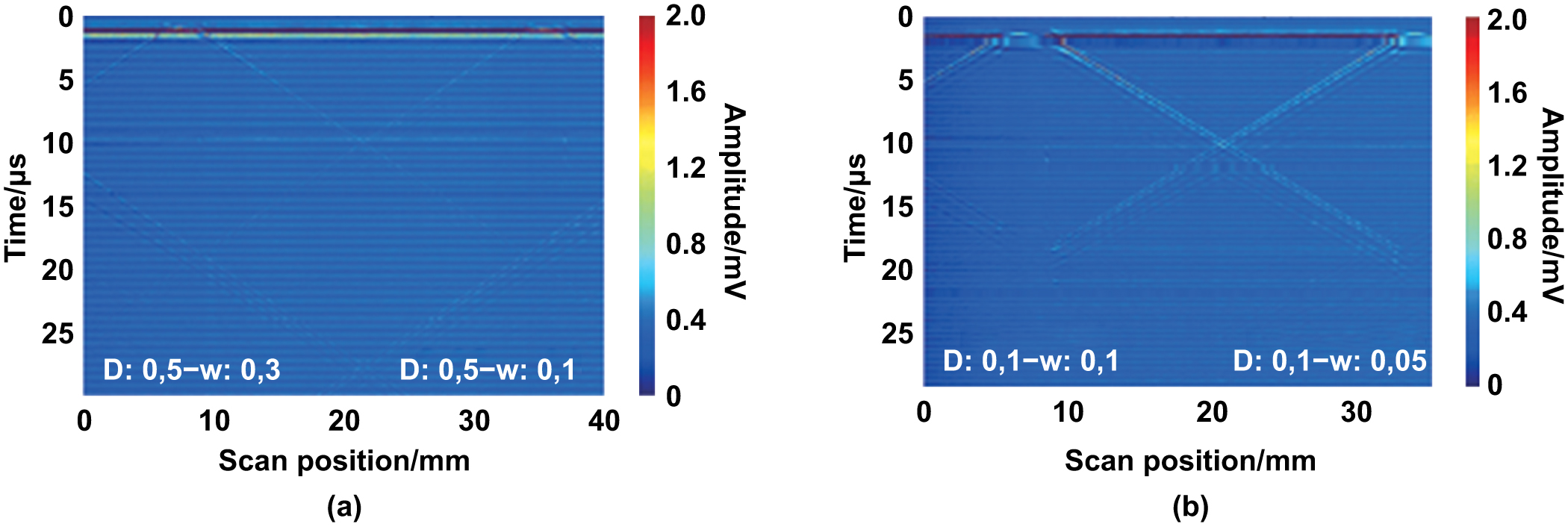
In addition to traditional ultrasonic inspection methods, laser ultrasonic inspection methods have better performance in defect detection. Millon et al [83] studied the laser ultrasonic detection method of crack defects. First, they used a pulsed laser (pulse time 7 ns) to generate ultrasonic waves in the part. Then they used a laser interferometer to detect the surface wave of the additively manufactured workpiece. Finally they used B-Scans to detect surface defects on the part, as shown in figure 9.
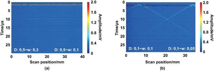
Figure 9. B-scans of defects with different depths: (a) defect depth 0.5 mm and (b) defect depth 0.1 mm [83].
Download figure:
Standard image High-resolution imageThe propagation of ultrasonic waves in additively manufactured parts will be affected by defects, so it can reflect defect information in parts. This method is mainly used to detect defects such as pores and cracks. Traditional ultrasonic testing inputs energy into the workpiece through a couplant. The application of this technology in AM defect detection is limited due to factors such as the temperature of the part. At the same time, the laser ultrasonic method has great potential in real-time defect detection. However, the aforementioned studies are still in the principle verification stage, and most of the workpiece surface needs to be processed to eliminate the influence of surface roughness.
4. Defect detection technology based on machine learning
Machine learning has developed rapidly in recent years. Significant progress has been made in object detection [84], intelligent robots [85], industrial quality inspection [86] and other fields. Deep learning uses multiple convolutional layers structured inside a neural network where input data characteristics are learned to process lower-level features into more abstract high-level features. These features are then used to classify data into categories learned from the training process. The results are expressed in the form of vectors, feature maps, etc. Based on the powerful learning ability and feature extraction of deep learning, many researchers have used this technology to detect defects and improve overall detection efficiency and quality [87–89].
Machine learning inspection is composed of two main processes: image acquisition and defect detection. Factors such as different image acquisition equipment, shooting angles, lighting conditions, and environmental changes give the acquired images different qualities, which determine the difficulty of the image processing degree. The feature extraction capabilities of different image processing algorithms and the pros and cons of image preprocessing methods directly affect the accuracy and false detection rate of defect detection.
4.1. Convolutional neural network (CNN) method
The use of convolutional neural networks (CNNs) [90] for defect detection can be summarized in two major scenarios. The first one consists of designing a complex, multi-layer CNN structure, then obtaining image features from a different network to finally perform image defect detection based on end-to-end training [91, 92]. In contrast, the second one combines the CNN with a Conditional Random Field (CRF) model, and either uses CRF energy functions as a constraint to train the CNN or optimizes network prediction results to conduct defect detection. In general, the advantages of CNNs include the network's strong ability to learn high-dimensional data in addition to abstract, essential, and high-level features from the input data. Some disadvantages are that the expressive power of the network increases as the depth increases. The deeper the network structure, the greater the computational complexity.
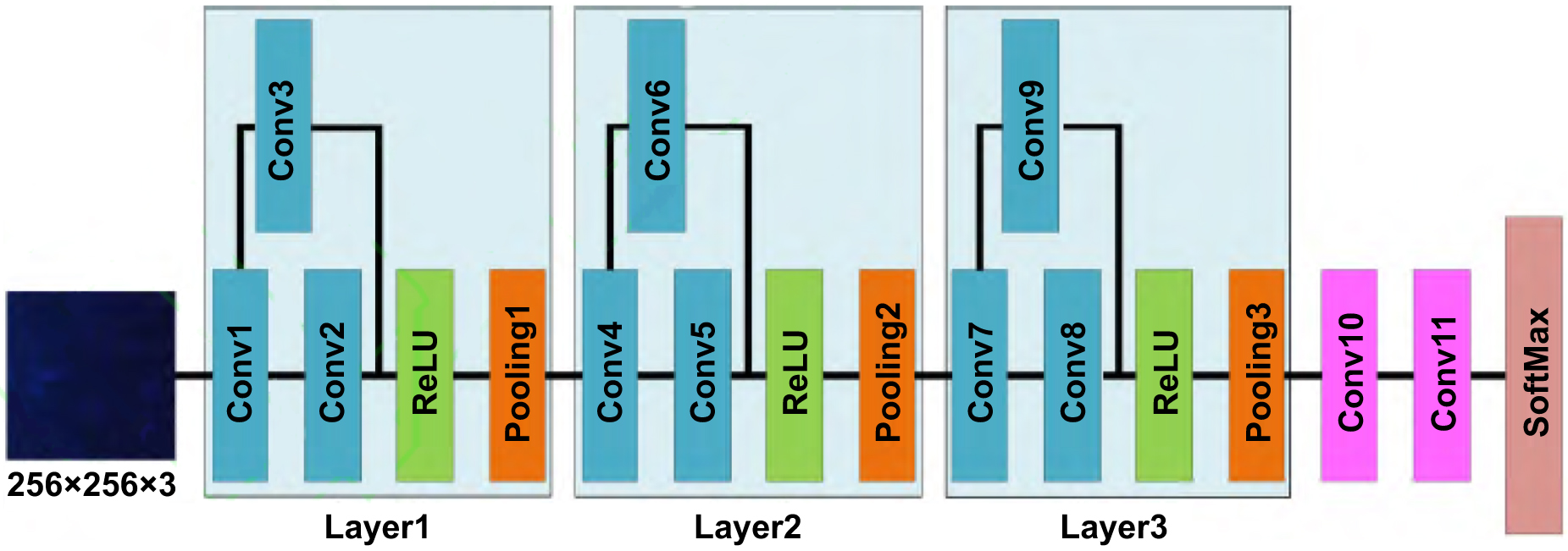
Xie et al attempted to detect surface defects in sheet metal parts by proposing a surface defect recognition and classification method for sheet metal parts based on CNNs [93], as shown in figure 10. The input image size was 256 × 256 × 3. As presented in figure 11(a), the defect samples were obtained through defect segmentation and extraction method, and the window sliding detection method was used. The entire image to be inspected was traversed through window sliding, and the region block of the window size was intercepted and compared to the model. The experiment was trained under a learning rate of 0.001, 0.001, and 0.001. The data in figure 11(b) shows that when the learning rate is 0.0001, the accuracy rate can reach 97.02%, and the average inspection time per piece was 0.85 s.
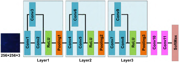
Figure 10. Convolution neural network structure [93].
Download figure:
Standard image High-resolution image
Figure 11. Surface detection effect display: (a) detection effect display and (b) comparison of the correct rate of different learning rates [93].
Download figure:
Standard image High-resolution image4.2. Auto-encode network method
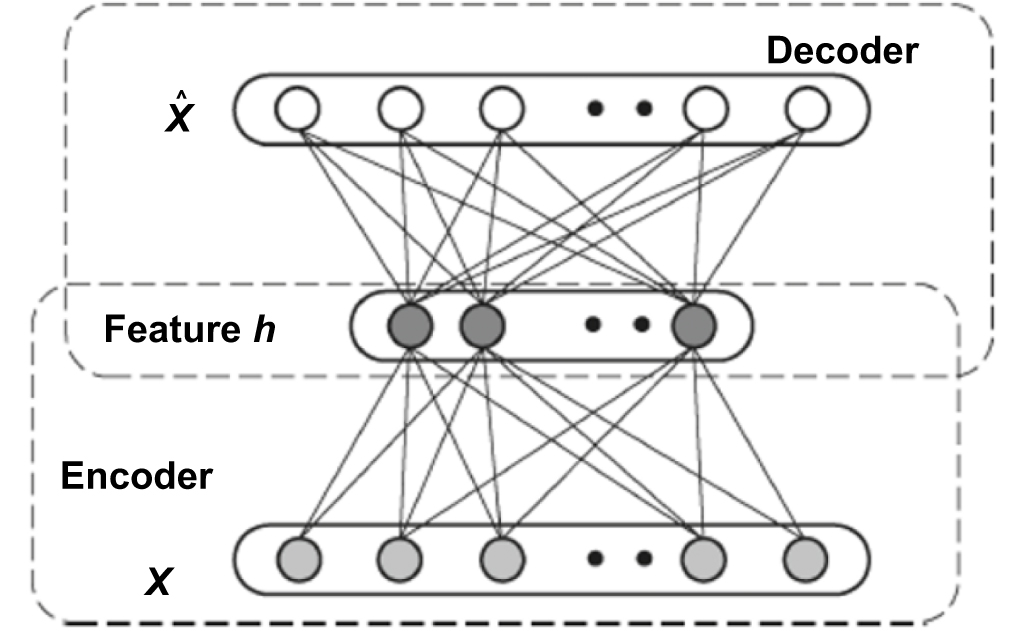
The Auto-encoder Network includes two stages: encoding and decoding. In the encoding stage, the input signal is converted into an encoded signal for feature extraction. In the decoding stage, the feature information is converted into a reconstructed signal, adjusted by weight, and offset. The reconstruction error is generally small, and defect detection is realized [94]. The biggest difference between the Auto-encoder Network and other machine learning algorithms is that the learning goal of the Auto-encoder Network is feature learning rather than classification. It has a strong independent learning capacity, high nonlinear mapping competence, and the ability to learn nonlinear metric functions to address the segmentation of complex background and foreground regions. It can effectively express target information, better extract the foreground area in a complex background, and has high robustness to environmental noise. A disadvantage of the Auto-encoder Network is that it requires consistent input and output data dimensions [95].
The Auto-encoder Network is an unsupervised learning network that consists of into two parts: an encoder and a decoder, which are composed of fully connected neurons, as shown in figure 12. Given the input space  and the feature space
  , the auto-encoder solves the mapping
  between the two to minimize the reconstruction error of the input features [96]:


Figure 12. Auto-encoder structure [96].
Download figure:
Standard image High-resolution imageAccording to equation (3), after the solution is completed, the hidden layer feature  output by the encoder (encoded feature) represents the input data
  .
.
4.3. Deep residual neural network method
Feature information in the CNN generative confrontation network increases as the depth of the network increases. However, it is easy to prevent the activation function from converging. The deep residual network uses residual optimization to continuously increase the number of network layers as the network structure increases, so the output of the convolutional layer in the residual unit has the same dimensions as the input elements. The activation function reduces loss [97]. An advantage of this operation is that the residual network has lower convergence, which improves classification performance while preventing excessive overfitting. A disadvantage is that the residual network must cooperate on a deeper level to give fully realize its structural advantages.
Che et al proposed an improved deep Residual Shrinkage Network model [98]. Assuming that the mapping required to be solved is  , this problem can be converted to solve the residual mapping function
  of the network, where
  . Compared with the Rectified Linear Unit (ReLU) function, soft thresholding provides a more flexible feature value interval. In the residual shrinkage network, the sample's situation can automatically adjust the threshold through the attention mechanism. A part of the deep residual shrinkage network model is shown in figure 13, where the size of the input
  is
is  , and
, and  is obtained as the input of the second layer through the ReLU function. By constructing a small sub-network in the second layer of the network, containing a set of threshold values
  , between 0 and 1, and then soft thresholding the features and adding the residual term
  , the output
  can be expressed as:


Figure 13. Model diagram of residual shrinkage network [98].
Download figure:
Standard image High-resolution imageEquation (7) is the soft threshold result obtained by comparing  in each dimension with the corresponding threshold
  .
.
4.4. Recurrent neural network method
A classic CNN model extracts the input layer test sample feature information through convolution and pooling operations. In contrast, a cyclic convolution neural network replaces the convolution operation in the CNN with a cyclic convolution operation. The difference is that after the recurrent neural network (RNN) performs a recurrent operation to extract input layer features, it does not perform a pooling layer operation to extract the features but uses a recurrent convolution operation to perform feature processing on the sample. On this basis, an advantage of the cyclic CNN is that it can learn the essential characteristics of data when the sample data is small, which reduces the loss of data information in the pooling process. A disadvantage is that as the number of iterations in the network training process increase RNN, the RNN model may appear over-fitted [99].
Zhang et al proposed an improved RNN model [100]. Due to the structural nature of ordinary RNNs, gradient disappearance and gradient explosion occurs when obtaining the derivative through the chain rule. In order to avoid such problems, a long short-term memory (LSTM) unit was added to improve the RNN. As shown in figure 16, the unit on the left of the figure 14 represents the calculation of this unit at the previous time, the unit in the middle represents the calculation at the current time, and the unit on the right represents the calculation at the following time.  represents the input of the unit and
  represents the state of the current unit. The input and output of the ordinary RNN unit can be modified to get the LSTM RNN.

Figure 14. LSTM RNN structure [100].
Download figure:
Standard image High-resolution image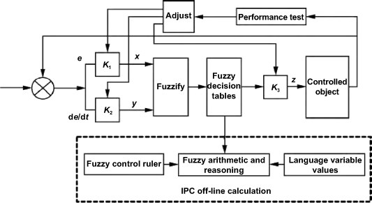
Figure 15. Diagram of the closed-loop adaptive fuzzy control system [101].
Download figure:
Standard image High-resolution image
Figure 16. Comparison of wire laying effects: (a) without closed-loop control system and (b) with closed-loop control system [101].
Download figure:
Standard image High-resolution imageIn figure 14,  represents the sigmoid activation function,
  represents the current hidden layer state, and
 represents the input of the current unit.
Due to the layer-by-layer manufacturing feature of AM, machine vision technology can be used to collect and analyze images layer by layer in the manufacturing process. For example, Sun et al of Zhejiang University proposed a multi-angle visual inspection technology for surface defects based on self-feature extraction in response to defects generated in the fused deposition modeling (FDM) process [102]. Zhang [103] applied machine vision technology to the online powder-deposition quality monitoring system of flexible laser melting molding. This system first captures the surface image of powder layer by an industrial camera, and then extracts and recognizes defects in the image by image processing and pattern recognition methods. There are other studies that combine machine vision technology and machine learning for defect detection [104, 105]. However, machine learning requires a large number of training samples, and reasonable training is needed to improve accuracy. In a specific AM process, the landing and adaptability of the application needs to be improved.
5. Latest research of defect detection technology
5.1. Advances in traditional defect detection technology
Scholars around the world have used various defect detection technologies, such as machine learning and laser detection methods, ultrasonic, pulse magnetoresistance, pulse eddy current, and far-field eddy current technologies. These technologies have mainly been used to identify defects in pipelines, aluminum materials, stainless steel, metal materials, welds, etc. Products in manufacturing-related fields, such as batteries, are tested for defects to improve the detection and classification capabilities of surface, subsurface, and internal defects of manufactured products. Machine learning is a widely used detection technology because it has the least impact on part contour, increased detection efficiency and is also highly automated compared to traditional inspection technologies.
Wen et al proposed the inclusion of a closed-loop adaptive fuzzy control system in a machine vision framework, to detect the effects of automatic wire laying (width of 6.35 mm and gap threshold of 0.1 mm) [101]. The frame diagram of the control system is shown in figure 15 and the results of the test comparison are shown in figure 16. Shi et al used the machine learning method to evaluate the efficiency of laser cleaning oxide films from an aluminum surface [106]. An algorithm called Retinex was used and reached a recognition efficiency of 86.70% and a detection accuracy of the surface oxide up to 0.03 mm. The total recorded processing time of a single sheet was 400 ms. A schematic diagram of the online detection system is shown in figure 17.

Figure 17. Schematic of the laser cleaning online detection system [106].
Download figure:
Standard image High-resolution imageZhou et al used a combination of pulse and eddy currents to detect surface and sub-surface defects on ferromagnetic products [107]. Extracting the spectral amplitude characteristics of aluminum and ferromagnetic products for neural network learning can detect subsurface crack defects. The influence of the composite signal of magnetic flux leakage and disturbances on the eddy current signal become smaller as the depth of the defect increases. The effect of using eddy current testing technology needs to be further improved for deeper defects. The pulsed eddy current three-dimensional detection model and experimental device are shown in figure 18.

Figure 18. (a) Pulsed eddy current three-dimensional detection model. (b) The experiment device [107].
Download figure:
Standard image High-resolution imageThe ultrasonic defect detection method is an inspection method of the test sample based on signal processing. Experimental results are mainly reflected in the performance of ultrasonic signals to determine defects in the product. Therefore, these summarized results do not provide specific indicators such as accuracy rate, recognition rate, or recall rate. It was found that the air-coupled ultrasonic Lamb wave detection method can effectively detect internal defects of metal plate structures. Meng et al used the imaging effect of the received signal to determine the actual defect location [108]. As shown in figure 19, the detection accuracy rate was 90.00%, the defect measurement error was ±0.01 mm, the axial resolution was 0.007b and the maximum measurement diameter was 30 mm.

Figure 19. Signal after window addition of a defect-free aluminum plate: (a) time domain diagram after window addition and (b) time frequency diagram after window addition [108].
Download figure:
Standard image High-resolution imageThe improved Gabor filter technology of Qu et al achieved an average detection speed of 91.80 ms/frame for defects such as scratches, holes, oxide skin, pitting, abrasions, edge cracks, and scars in steel materials [109]. The average detection accuracy was 95.80%. This method has a high recognition accuracy for defect detection but can only detect defects on the surface of the product. The detection and recognition results of this algorithm are shown in figure 20.
Figure 20. Gabor wavelet defect detection images [109].
Download figure:
Standard image High-resolution imageThe x-ray inspection technology has a better recognition effect on defect edge detection. The technology of Tian et al effectively detected the edges of pipeline surface defects and dynamically extracted weld features [110]. The test results are shown in figure 21.
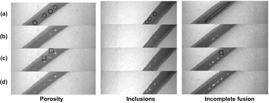
Figure 21. Defect detection results for three images, using the x-ray method [110].
Download figure:
Standard image High-resolution imageLiu et al used x-ray images and CNNs to detect and identify surface and internal defects of petroleum steel pipe welds [111]. X-ray images of petroleum steel pipes were used as inputs to detect and recognize weld defects. The OPTICS algorithm based on density clustering was used to obtain clusters of arbitrary density to separate defects and noises of various shapes and sizes. The use of the CNN method broke through the manual feature extraction bottleneck, improved the degree of automated classification, and achieved a high recognition accuracy rate. The detection image and network structure diagram are shown in figure 22.
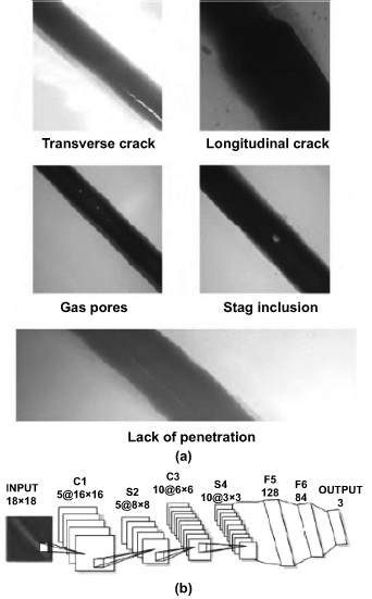
Figure 22. (a) Diagrams of x-ray weld defects (various welding defects). (b) Structure diagrams of the CNN [111].
Download figure:
Standard image High-resolution imageIn addition to the above-mentioned defect detection methods in manufactured products, additional technologies, namely clutter suppression and the least squares method [112], have been developed by researchers for the same purpose. Results of a combined algorithm of these two methods, for the detection of surface defects in scanned images, indicate that the least squares method was capable of eliminating the through wave and ground reflection wave from processed images, which is convenient for extracting defect characteristics.
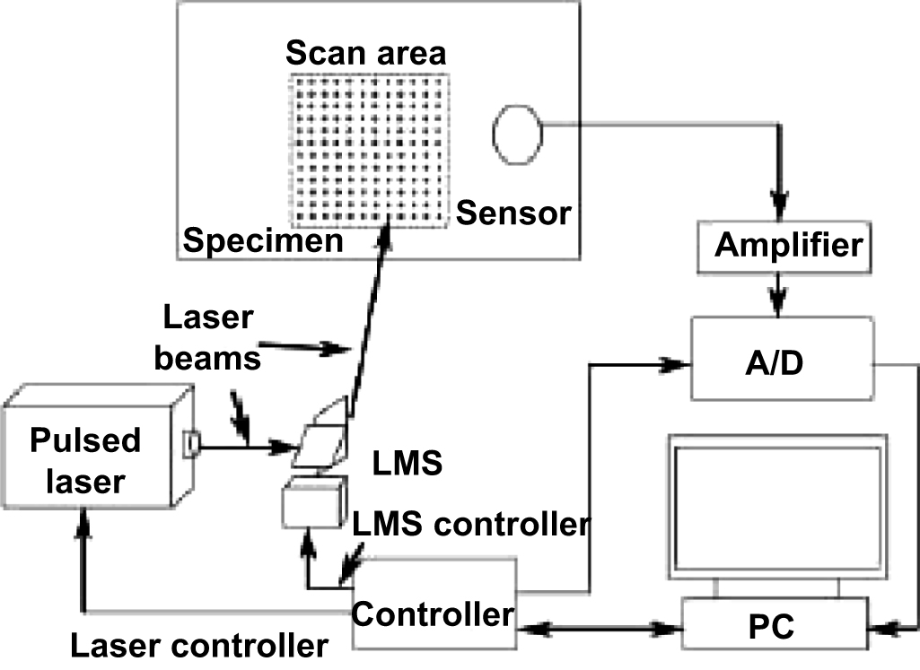
Chi et al proposed an improved ultrasonic diffraction time difference technique for detecting surface defects on aluminum alloy plates [113]. Their results show that defects with a depth of 1.9 sm and 6.2 sm were more clearly detected. In [114], ultrasonic waves using the Hilbert transformation were used to detect the surface and internal defects of metal materials. Their results suggest that this method has a can detect the shape, size, and distribution of defects. The Hilbert method of transforming the ultrasonic signal not only effectively extracts the information of the ultrasonic signal propagating on the defect, but also intuitively and efficiently detects the shape, size, and distribution of surface defects from the image of the ultrasonic propagation. The inspection system is shown in figure 23.

Figure 23. Laser ultrasonic inspection system [114].
Download figure:
Standard image High-resolution imageAlthough these methods are theoretical, they have obtained promising detection results. Therefore, these studies can provide both theoretical and practical guidance for future defect detection attempts of manufactured products.
5.2. Advances in deep learning defect detection
With the development of artificial intelligence, deep learning methods have been widely used in product defect detection due to their ability to fit arbitrary complex functions and perform proficient feature extraction. In recent years, the technology innovation of deep learning has mainly focused on high precision, high positioning, rapid detection, small targets, and complex background detection.
Chen et al attempted high-precision target detection [115]. A convolutional layer from an ordinary classification network was used to obtain a feature map of the sample. Then a region of interest algorithm was used to identify the target object to be tested in this feature map to improvement the target detection accuracy.
Redmon et al proposed candidate boxes proposed [116] for the feature selection of objects to test the performance of a binary classification function for fast target detection. Multi-scale prediction was used to accurately determine the predicted position. Fu et al developed end-to-end small target detection and end-to-end thinking [117] combined with position regression and semantic information. These were merged and set as underlying network features to improve the ability to identify small targets.
Ma et al proposed the LCD surface defect detection model based on small sample learning was proposed to develop a training network strategy based on small samples [118]. The model was characterized by automatic segmentation and positioning preprocessing software that divides high-resolution images into image sub-blocks suitable for CNN learning. Image sub-blocks were obtained according to the model's judgment category and positioning coordinates, and multiple types of defects were detected. The feature map generated in this experiment is shown in figure 24.

Figure 24. Feature map of bump defect [118].
Download figure:
Standard image High-resolution imageDai et al presented t deformable CNNs and regions of interest to improve the ability to detect irregularly shaped objects against complex backgrounds, improving target detection with unbalanced data samples and diverse detection targets [119]. Bodla et al proposed a measurement method that detects targets by making associative relationships between objects [120]. The association information is integrated into the extracted features and feature dimensions are kept unchanged, which improves the similarity of the objects. The feature recognition ability varies with time.
Liu et al proposed a method [121] detects end face defects in tiny cylinder core blocks with complex backgrounds. In general, the usage of traditional segmentation, where thresholding, morphology and Canny edge detection are used to treat grayscale information representative of uneven surface features, is imprecise. Therefore, the authors proposed defect detection using structured light triangulation and processing based on machine learning algorithms. This method has a high recognition rate for defects hidden in cluttered backgrounds, and the repeatability can reach sub-pixel levels with good anti-interference and practicality. The acquisition device and detection structure are shown in figures 25 and 26.

Figure 25. (a) Ordinary light source. (b) Left structure light. (c) Right structure light. (d) Diagram of the acquisition device [121].
Download figure:
Standard image High-resolution image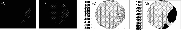
Figure 26. (a) Approximate area of defects. (b) Intersection scatter plot. (c) Delaunay triangulation. (d) Exact area of defects [121].
Download figure:
Standard image High-resolution image
6. Future prospects for defect detection technology
Research in quality-related fault prediction and diagnosis technology remains at a preliminary stage of exploration. If we want to apply the detection technology to the AM field, these technologies should be based on the industrial characteristics of AM from the analysis and improvement of data sets, image acquisition methods, and detection scheme design. Therefore, it is necessary to conduct an in-depth analysis on the feedback related to AM defect detection and fault prediction and diagnosis technology.
Deep learning is essentially data-driven. If we want to establish a deep learning model applicable to AM, we need a large number of different AM product angles, positions, sizes, shapes, and other information with a relatively small amount of data. While CNNs, auto-encode networks, deep residual networks, and RNNs have their own advantages and disadvantages, obtaining a universal deep learning model for AM product defect detection is a difficult task that must be further studied.
There is a large amount of concentrated energy input in the AM process. The material reaction process and the molten pool environment are complicated, and the products' temperature fields are difficult to control. Many factors work together to make the detection environment more complicated. In the image acquisition process, the apparent characteristics of the target object change significantly with different lighting conditions, imaging angles of view and shooting distances. Noise interference and partial occlusion of the detected sample can occur due to variations in the detection target's background. Therefore, methods to improve the accuracy of AM defect detection in samples based on the efficient feature extraction capabilities of deep learning need more consideration.
Current traditional defect detection methods are mainly aimed at the detection of object surface defects in two-dimensional images, which are usually surface scratches and abrasions. However, the viewing angle information obtained by the two-dimensional image sequence only supplies information in a single direction, limiting the available data and preventing the collection of information from other viewing angles. However, the shape of processing defects in AM is more complex. Therefore, the usage of multi-cameras to model products in three dimensions must be investigated in order to express information more clearly and from various perspectives for the improvement of defect detection accuracy.
As manufacturing companies regard defect detection as a task of primary importance, we also hope to realize online, real-time monitoring of production defects in AM through embedded sensing equipment. Combining smart sensors and mechanical devices to achieve multi-modal, real-time defect detection of manufactured products will benefit factory applications.
At the same time, most of the existing defect detection methods only use traditional industrial processing and manufacturing fields. The detection data and detection methods collected in the AM processing field can be replaced. Therefore, more traditional detection technologies should be explored. Machine learning detection is based on characteristics of the AM field and rely on the methodology and experience of traditional machining defect detection. As a result, machine learning represents the most suitable AM defect detection program.
7. Conclusions
AM technology is considered one of the most promising manufacturing technologies due to its unique advantages over conventional subtractive manufacturing processes in terms of customization, complex geometry, and near-net-shape fabrication in the aerospace and defense industries. Although the development of AM technology has been relatively successful at attaining sufficient mechanical properties, defects and poor geometric accuracy limit actual component adoption in the industry. Some defects that appear in general AM processes include cracking, residual stresses, porosity, and balling. Furthermore, as defects often occur in the build component due to discontinuities that originate during the printing process as a result of numerous factors, the development of novel defect detection technologies has recently surged in the AM field. Based on detection and classification performance, different traditional and machine learning detection technology are summarized. This paper also discusses the latest research and the future prospects of defect inspection technology.
Acknowledgments
The authors would like to express their sincerest gratitude for the financial support of the National Key R&D Program of China (Project Nos. 2017YFA0701200, 2016YFF0102003), the Shanghai Science and Technology Committee Innovation Grant (Grant Nos. 19ZR1404600, 17JC1400601), and the Science Challenging Program of CAEP (Grant No. JCKY2016212A506-0106).