

Abstract
With the rapid emergence of in-memory computing systems based on memristive technology, the integration of such memory devices in large-scale architectures is one of the main aspects to tackle. In this work we present a study of HfO2-based memristive devices for their integration in large-scale CMOS systems, namely 200 mm wafers. The DC characteristics of single metal–insulator–metal devices are analyzed taking under consideration device-to-device variabilities and switching properties. Furthermore, the distribution of the leakage current levels in the pristine state of the samples are analyzed and correlated to the amount of formingless memristors found among the measured devices. Finally, the obtained results are fitted into a physic-based compact model that enables their integration into larger-scale simulation environments.
Export citation and abstract BibTeX RIS

Original content from this work may be used under the terms of the Creative Commons Attribution 4.0 licence. Any further distribution of this work must maintain attribution to the author(s) and the title of the work, journal citation and DOI.
1. Introduction
The imminent end of Moore's law and the exponential growth of data generation due to worldwide digitalization are already causing noticeable consequences to machine learning development. Emerging artificial intelligence (AI) applications such as, for instance, autonomous driving and biometric recognition, require power hungry processors that are able to deal with considerably large amounts of data stored in remote and enormous server racks that analogously, exhibit high power consumption and expensive maintenance. Moreover, the so called von Neumann bottleneck, derived from data throughput limitations due to the implementation of traditional computer architectures, is gradually hindering AI progress as well. In-memory computing and its upcoming focus on AI applications are potentially the next step in the future of data computation and the most suitable computing architecture to overcome such problems [1, 2].
Memristors (memory resistors) have become a promising alternative to conventional non-volatile memories (NVM) and are proven to be a suitable building block in the basis of in-memory computing systems. This is feasible since this emerging technology is currently allowing the development of systems featured by low power consumption, low latency and high scalability in neuromoprhic computing for AI applications, logic in memory and cybersecurity, among many others [3–8].
The integration of memristors in large-scale neuromorphic systems is one of the main incentives to enhance the technology to a level that enables mass production of memristive-based systems. Reaching such technological maturity requires intensive device engineering and research at different abstraction levels i.e., from the study of device's material to larger composite systems. In line with this statement, in our previous works we analyzed the electrical properties of memristive cells integrated in one-transistor-one-resistor (1T1R) structures considering different material compositions [9–12]. Moreover, the impact of different programming algorithms on the performance of the mentioned structures was further studied and assessed in terms of their multilevel-capabilities [13, 14]. The obtained results were used to build and tune RRAM models [15, 16] and to assess the behavior of the multilevel-cell (MLC) approach in AI applications [17].
In accordance with these studies, this work presents, for the first time in the IHP technology, a wafer scale study of single metal–insulator–metal (MIM) memristive devices for their integration in large-scale CMOS systems. This work may reinforce the knowledge about the bi-level behavior of single memristive devices as foundation of further studies ultimately focused on more complex structures and multi-level approaches. For the sake of completeness, it is taken under consideration two different insulator layers, namely pure HfO2 (HfO) and Al-doped HfO2 (HfAlO), the latter being demonstrated to enhance the memristor's properties among other dielectrics, for instance thermal stability, retention [18], reduction of cycle-to-cycle and device-to-device (D2D) variability [9]. We focus on the bipolar switching of single memristors between a high resistance state (HRS) and a low resistance state (LRS) and vice versa. This switching phenomenon is achieved thanks to the creation and disruption of conductive filaments (CFs) in the insulator layer of the MIM stack. These are initially electroformed when a soft breakdown during the forming operation is induced by generating appropriate electric fields between the metal layers. This physical phenomenon is enhanced by electrical Joule heating as demonstrated in [19, 20]. Those CFs are constituted by oxygen vacancies driven toward the bottom electrode of the stack. During a reset operation, a negative voltage is applied between the two metal layers in order to disrupt the conductive paths, moving the memristor in HRS. On the contrary, a set operation is performed when a positive voltage is applied to the memristor and the vacancies filaments are rebuilt, switching the device to LRS.
Integration of such memristive devices in larger-scale systems requires accurate mathematical models able to reproduce their physical properties in circuit simulators. Thus, the electrical characterization carried out in this study also allowed us to tune the standard Stanford Model [21] to both technologies considered in this paper. The fitted physic-based memristor model can be further integrated in larger scale systems for high scale simulations as demonstrated in [22].
The physical characteristics of the analyzed samples and the measurement methodology are described in section 2. In section 3, it is given a brief introduction to the fundamental equations governing the memristor model adapted to the empirical results. Section 4 summarizes the main electrical results and their further analysis, as well as the corresponding simulated results. Finally, the main conclusions are drawn in section 5.
2. Experimental methodology
This study was performed over single MIM cells integrated into two different 200 mm wafers. Wafer 1 integrates TiN/HfO2/Ti/TiN stacks and wafer 2 integrates TiN/Al:HfO2/Ti/TiN stacks. Both stacks are composed by TiN top and bottom electrodes of 150 nm thickness and a Ti layer of 7 nm thickness deposited by sputtering. The Ti layer acts as an oxygen scavenging layer that enables the resistive switching properties of both insulator layers, namely HfO2 and Al:HfO2 [23, 24]. Wafer 1 contains a pure HfO2 layer of 8 nm, whereas wafer 2 is composed by an Al-doped (about 10%) HfO2 layer of 6 nm, both deposited by atomic layer deposition (ALD). The MIM cells are fabricated with an area of about 0.4 μm2.
Both wafers are divided into 108 dies which contains 20 MIM devices each. A total number of 2160 samples are fabricated per wafer. Considering the present study, one sample per die is characterized. A total number of 213 MIM samples were tested, out of which 106 correspond to wafer 1 (HfO) and 107 to wafer 2 (HfAlO).
The results exposed below were obtained using the following DC approach: first, the leakage current of the pristine state of the samples is measured applying a voltage ramp from −0.3 to 0.3 V. The measured current gives us a hint about the insulation level between the two metal layers prior to the formation of the CFs, as it will be described in section 4. Next, with the forming operation the cell is moved into LRS for the first time by applying a positive voltage sweep between 0 and 5 V with steps of 0.05 V and a slope of around 300 mV s−1, setting a compliance current of 200 μA. The reset operation is performed applying a negative voltage sweep between 0 and −1 V in steps of 0.01 V. In order to ease the transition to HRS, we do not impose a compliance current during this operation. Finally, the set operation to switch the device to LRS is performed applying a positive voltage sweep between 0 and 1 V in steps of 0.01 V imposing a compliance current of 300 μA. For both set and reset operations the voltage slope is also 300 mV s−1. Once the sample is correctly switched between both resistance states, 100 reset/set cycles are performed.
3. Modeling methodology
The memristor model used to reproduce the experimental results obtained using the methodology described above is the standard Stanford model [21]. Among a wide variety of physic-based compact models [25], this model features a good trade-off between computational cost and simulation accuracy, allowing to execute up to thousand devices in a reasonable simulation time. It mimics the behavior of memristive devices based on the gap distance (g) between the tip of a single CF and the opposite electrode. Depending on the applied operation, the gap distance increases (reset) or decreases (set), setting the device into HRS or LRS, respectively. This gap evolution is mathematically described in equation (1).

where ν0 is a fitting parameter that accounts for the velocity dependent on the attempt-to-escape frequency, kb is the Boltzmann constant, Ea is the effective activation energy for vacancy generation, a0 is the atom spacing, q is the electron charge, V is the voltage applied to the device, tox is the dielectric thickness and T is the device temperature. The variable γ is the field local enhancement factor that accounts for the material polarizability [26]. Considering bipolar switching, both LRS and HRS are defined by the gap boundaries, namely gapmin and gapmax, respectively. Finally, the resulting current flowing through the cell (I) is computed as it follows:

where I0, g0 and V0 are fitting coefficients tuned to achieve the appropriate response.
In order to speed up the fitting procedure, the Stanford model was integrated into a Matlab app which features an user friendly GUI and low computational complexity. This allows the user to easily tune the parameters of the model and observe the corresponding variation of the IV characteristics in a intuitive way. The obtained results were assessed in a circuit simulation environment such as Cadence where the model was implemented in VerilogA.
4. Experimental and modeling results
In this section, it is exposed the main results gathered from the electrical characterization carried out following the methodology described in section 2. First, the distribution of the pristine state currents of all devices integrated in both wafers were analyzed. Afterward, the D2D variability featured in both technologies under study is analyzed considering memristive properties such as forming voltage (Vform), set voltage (Vset), reset voltage (Vreset) and memory window (MW). These parameters are analyzed and compared among the two technologies. Finally, considering the reset/set experimental data, the Stanford model briefly described in section 3 is adapted to both technologies by means of two different sets of parameters.
4.1. Experimental characterization
The pristine state current, also known as leakage current, is the measured current through the MIM stack before the formation of the CFs in the insulator layer. As mentioned in section 2, this current is an indicator of the voltage level required to form the conductive paths in a further forming operation. As demonstrated in [27] and also in our results exposed below (see figure 2), the higher the pristine state current of the sample, the lower the voltage required to form the device. This phenomenon is linked to the oxygen vacancies distribution in the hafnia layer.
Considering the samples in this work, figure 1 shows two heat maps depicting the pristine state current distribution along the wafers under study. The warmer the displayed color, the higher the measured pristine state at 0.2 V. Each die within the plots represents a single MIM sample. It can be appreciated that HfAlO wafer (figure 1-right) presents a higher number of leaky samples. That is, the number of samples that present a high pristine state current (considered to be over 10 nA) in the HfAlO wafer is 44 (41%), whereas the number of leaky samples in the HfO wafer (figure 1-left) is only 4 (3.8%). It has been demonstrated that doping HfO2 with Al increases the atomic concentration of the material [18] and thus, it enhances the uniformity of the distribution of oxygen vacancies in the pristine state of the insulator layer. This might ease the creation of 'weak' conductive paths (also known as 'percolation paths' [28]) by thermal effects in the fabrication process. This causes an increment in the leakage current measured in the pristine state of the leaky samples. Due to the stochastic nature of the devices [29], those conductive paths might not be created and therefore, samples that present low leakage current can also be found. On the other hand, most samples with pure HfO2 layers do not exhibit high leakage current in their pristine state and thus, uniform oxygen vacancies distribution.
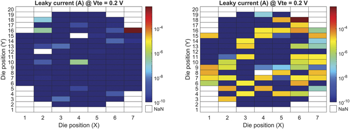
Figure 1. Pristine state current distribution along wafers containing HfO (left) and HfAlO (right) samples.
Download figure:
Standard image High-resolution imageRight after measuring the leakage current, a forming operation followed by applying a positive voltage ramp to the top electrode of the cells. In this way, a soft breakdown is induced to build for the first time the CFs through the insulator layer. Figure 2 exposes the correlation between the pristine state current level and the forming voltage required to switch the devices to LRS. It can be observed that samples with high pristine state current, mostly found in HfAlO wafer, present low forming voltage or even 'formingless' behavior, compared to the samples with low pristine state current. For this reason, from now on in the DC analysis that proceeds, the samples are divided into three sets: HfO, HfAlO with high leakage current (HfAlO-hlc) and HfAlO with low leakage current (HfAlO-llc). Following this classification, figure 3 shows the forming voltage reported by the samples considered in each set. It is shown that HfAlO-hlc samples account for the lowest forming voltages, that is to say Vform ranging between 0.5 and 1.5 V. On the other hand, HfO samples present a forming voltage between 1.75 and 3.25 V accordingly to their lower leakage currents. Besides, HfAlO-llc samples are formed in a range between 2.5 and 4.25 V. The existence of weak conductive paths in the pristine state of HfAlO-hlc memristors may lead to low forming voltages in this set of samples [30, 31]. Due to the inherent stochastic behavior of HfO2-based memristors [29], both HfAlO-llc and HfAlO-hlc samples can be found within the same wafer.

Figure 2. Pristine state current measured at V = 0.2 V versus the corresponding forming voltage of HfO samples (red) and HfAlO samples (blue). On the left and right side of the dividing line located at 10 nA, the LLC samples and HLC samples are considered, respectively. Due to limitations in the measurement tool, the lowest pristine state current measured is 100 pA.
Download figure:
Standard image High-resolution image
Figure 3. Forming voltage distribution of HfO samples (a), HfAlO-llc samples (b) and HfAlO-hlc samples (c).
Download figure:
Standard image High-resolution imageOnce all the MIMs were initially set to LRS by means of the forming operation, we performed a first reset/set cycle to stabilize the CFs [32]. Afterward, 100 reset and 100 set operations are carried out over each cell in order to study their switching capabilities and the inherent variability exhibited by the three sets of samples. In total 90 out of 106 (85%) HfO samples passed the endurance test as well as 98 out of 107 (92%) HfAlO samples. Within the second group, 44 presented high leakage current (HfAlO-hlc) and 54 low leakage current (HfAlO-llc). Figure 4 shows the IV characteristics gathered from executing 100 reset/set cycles in each mentioned kind of sample.
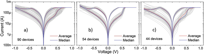
Figure 4. IV characteristics of HfO samples (a), HfAlO-llc samples (b) and HfAlO-hlc samples (c). The median value computed out of 100 cycles in each single device is displayed in gray, whereas the D2D average and median are plotted in red and blue, respectively.
Download figure:
Standard image High-resolution imageIt can be appreciated in this figure that, in general terms, the set of samples that presents the highest D2D variability is HfAlO-hlc, followed by HfO samples and finally, HfAlO-llc, being the set that reports the lowest D2D variability.
Concerning the reset and set voltages, figure 5 summarizes the distribution of such parameters for all the samples considered in this study. For the three sets of samples, the reset voltage presents generally lower variability than the set voltage. This could be clearly appreciated in HfO samples (see figures 5(a) and (d)) and HfAlO-hlc samples (see figures 5(c) and (f)). On the other hand, HfAlO-llc samples present less D2D variability in terms of Vset rather than Vreset (see figures 5(b) and (e)). The three sets report similar average Vreset values. However, in terms of Vset, due to the high variability presented by HfO and HfAlO-hlc, it cannot be compared with accuracy.
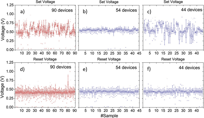
Figure 5. Vreset and Vset of HfO samples (a), (d), HfAlO-llc samples (b), (e) and HfAlO-hlc samples (c), (f).
Download figure:
Standard image High-resolution imageFigure 6 compares the LRS and HRS current values measured at 0.2 V and therefore, the corresponding memory window of the samples under study.
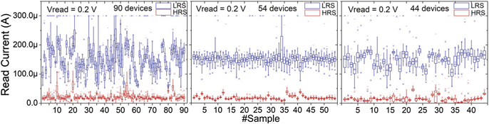
Figure 6. LRS (blue) and HRS (red) currents measured at Vread = 0.2 V in HfO samples (left), HfAlO-llc samples (middle) and HfAlO-hlc samples (right).
Download figure:
Standard image High-resolution imageIn line with figures 4 and 6 clearly exposes the higher variability measured in HfO and HfAlO-hlc with respect to HfAlO-llc. In average terms, MW (ILRS/IHRS) is computed to be around 10 in HfAlO-llc samples, 11 for HfAlO-hlc samples and around 8 for HfO samples.
It can be appreciated that, in general, there is a trade off in terms of electrical properties between HfAlO-llc and HfAlO-hlc samples. On the one hand, HfAlO-hlc samples present 'formingless' characteristics, which can enhance their integration in larger CMOS systems. The lower range of forming voltages compared to HfAlO-llc can reduce the electrical requirements of the memristive-based integrated circuits, lowering the voltage ranges needed to operate them. On the other hand, the higher ranges of forming voltages reported by HfAlO-llc samples may require of dedicated circuits to carry out the forming operations. These are only used at the beginning of the lifetime of the memristors and they feature higher electrical constrains. On top of that, they also tend to occupy larger chip area. However, HfAlO-hlc samples present lower yield in terms of electrical properties. The higher D2D variability due to multiple dominant CFs may diminish the global performance of the memristive-based systems in which they are integrated. Therefore, the trade off between low forming voltages and more reliable electrical properties must be taken into account for the integration of such memristors in larger-scale circuits.
4.2. Modeling results
As described in section 3, the standard Stanford Model was tuned to reproduce the experimental results analyzed above. More precisely, the global median curves (blue line) represented in figures 4(a) and (b) are used as reference. These are computed from all the 100 reset/set cycles carried out in each of the samples within the HfO and HfAlO-llc samples. Tables 1 and 2 gather the main parameters chosen to simulate the DC response of HfO and HfAlO-llc samples, respectively.
Table 1. Fitting parameters for Stanford model to simulate HfO samples.
| g0 = 0.53 nm | V0 = 0.3 V | I0 = 300 μA |
| υ0 = 80 m s−1 | β = 5.3 | α = 2.3 |
| gapini = 0.35 nm | T0 = 300 K | γ0p = 22 |
| gapmax = 1.5 nm | tox = 8 nm | γ0n = 15.3 |
| gapmin = 0.25 nm | Ea = 0.6 eV | Rth = 1500 K/W |
Table 2. Fitting parameters for Stanford model to simulate HfAlO-llc samples.
| g0 = 0.5 nm | V0 = 0.27 V | I0 = 300 μA |
| υ0 = 80 m s−1 | β = 5.2 | α = 2.1 |
| gapini = 0.45 nm | T0 = 300 K | γ0p = 22 |
| gapmax = 1.3 nm | tox = 6 nm | γ0n = 15.3 |
| gapmin = 0.25 nm | Ea = 0.6 eV | Rth = 1500 K/W |
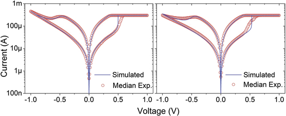
Due to the low yield in terms of electrical properties presented by the HfAlO-hlc samples, the model was only adapted to the two previously mentioned experimental sets of samples. Therefore, figure 7 exposes the simulated results in comparison with the median experimental curves. For both technologies, it can be appreciated that the model is able to reproduce in an accurate way the two resistance levels as well as the electrical characteristics analyzed in section 4.1, namely set/reset voltages and memory window.
Figure 7. Median experimental (red circles) versus simulated (straight blue line) results from HfO (a) and HfAlO-llc (b) samples.
Download figure:
Standard image High-resolution image
5. Conclusion
In this work, we performed a wafer scale study of HfO and HfAlO-based single MIM cells for their large-scale CMOS integration. The study was segregated in three different sets of samples based on the technology and the so called 'formingless' feature. The correlation between the leakage current in the pristine state of the samples and their forming voltages was assessed. This would shed light on the upcoming study and manufacturing of formingless samples whose lower voltage requirements are of high interest for the integration in large scale systems. Moreover, the IV characteristics of the samples were analyzed in depth taking into account different memristive properties that should be considered for in-memory computing applications. In general terms, HfAlO-llc samples present lower D2D variability, which can be translated in higher yield and better performance in certain neuromorphic applications for AI purposes. On the other hand, we found out that HfAlO-hlc samples present a higher D2D variability. This could be connected to the presence of multiple dominant conductive paths already formed during the fabrication process. In terms of electrical performance, these samples, as well as HfO samples could be suitable for their integration in system based on stochastic learning, as demonstrated in our previous studies [33]. Finally, the standard Stanford Model was adapted to both technologies enabling the integration of such experimental results in circuit simulation environments for their integration in larger CMOS-based system simulations.
Acknowledgments
This work was supported in part by the Deutsche Forschungsgemeinschaft (German Research Foundation) under Project 434434223-SFB1461 and in part by the Federal Ministry of Education and Research of Germany under Grant Numbers 16ES1002, 16FMD01K, 16FMD02 and 16FMD03.
Data availability statement
The data that support the findings of this study are available from the corresponding author upon reasonable request.