

Abstract
In recent years, topological quantum materials (TQMs) have attracted intensive attention in the area of condensed matter physics due to their novel topologies and their promising applications in quantum computing, spin electronics and next-generation integrated circuits. Scanning tunneling microscopy/spectroscopy (STM/STS) is regarded as a powerful technique to characterize the local density of states with atomic resolution, which is ideally suited to the measurement of the bulk-boundary correspondence of TQMs. In this review, using STM/STS, we focus on recent research on bismuth-based TQMs, including quantum-spin Hall insulators, 3D weak topological insulators (TIs), high-order TIs, topological Dirac semi-metals and dual TIs. Efficient methods for the modulation of the topological properties of the TQMs are introduced, such as interlayer interaction, thickness variation and local electric field perturbation. Finally, the challenges and prospects for this field of study are discussed.
Export citation and abstract BibTeX RIS

Original content from this work may be used under the terms of the Creative Commons Attribution 4.0 license. Any further distribution of this work must maintain attribution to the author(s) and the title of the work, journal citation and DOI.
Future perspectives
The experimental realization of novel topological quantum materials (TQMs) including strong topological insulators, weak topological insulators, quantum spin Hall insulators, quantum anomalous Hall insulators and topological semi-metals, has been extensively explored to catch up with the development of topological theories in recent decades. The gap between the applications and the fundamental properties of these TQMs is their stability in the environment of their practical use, where the thermal perturbation at room temperature may break the topological surface/edge states. Seeking new materials with a large topological gap or modulating the existing TQMs in various ways, such as element doping, strain effect, electric/magnetic field and light, is regarded as an effective path to promote their applications. This paper provides a brief overview of the bismuth-based TQMs studied by experimental technique, scanning tunneling microscopy, and an outlook based on this research to attempt to propose a viewpoint of the experimental part of the realization of novel TQMs as well as their practical applications.
1. Introduction
In recent decades, the exploration of topological quantum materials (TQMs) has evoked tremendous interest in condensed matter physics, which has benefitted from the rapid development of theoretical and experimental endeavors to understand their novel electronic topologies. To date, there has been a huge family of TQMs, including topological insulators (TIs), topological crystalline insulators (TCIs), topological semi-metals (TSMs), and topological superconductors [1, 2]. These TQM-based electronic devices possess great potential applications. In fact, TIs exhibit robust boundary states, which possess spin-momentum locked electrons and survive under moderate disorder as a consequence of their electronic wavefunctions, representing a promising candidate for spin-based spintronics and quantum computers [3, 4]. Based on the Bernevig–Hughes–Zhang model, different topological classes can be achieved by controlling the band inversion between the conduction and valence bands with different band parities and strong spin–orbit coupling (SOC) [5]. The strong SOC normally provides a large band inversion energy, which is essential for the modulation of topological properties and potential applications, as shown in figure 1. For example, a large gap of TIs exceeding the thermal excitation energy (∼26 meV) at room temperature is expected to be induced by strong SOC, which provides a large enough energy space for the survival of robust topological nontrivial edge states and promises applications in electronic devices from thermal perturbations even at high temperatures. The strength of the SOC is proportional to the  , where
  is the atomic number of an element. Bismuth (Bi), the heaviest non-radioactive and non-toxic element is regarded as an ideal component of the TQMs due to its large SOC strength. Bi-based TQMs ranging from quantum spin Hall insulator (QSHI), strong topological insulator (STI), weak topological insulator (WTI), high-order topological insulator (HOTI) and TSM, have been widely explored and intensively studied in both elemental Bi and its compounds in recent years [6–10].

Figure 1. (a)–(c) Schematic of the band structure of 2D normal insulators (NIs), Dirac semimetals (DSMs) and TIs, i.e. QSHIs, respectively. kx and ky represent the reciprocal lattice vectors of 2D Brillouin zone. Upper yellow bands and lower green bands represent 2D bulk bands, and the 1D red and blue lines in (c) are denote the 1D TES. (d)–(g) Schematic of the band structure on the top and side surfaces of 3D NIs, DSMs, WTIs, and STIs, respectively. Upper yellow bands and lower green bands represent the projection of 3D bulk bands to 2D surfaces, while the 1D red and blue lines in (f), (g) represent the 2D surface states.
Download figure:
Standard image High-resolution imageThere are several kinds of techniques to investigate the electronic features of TQMs, including angle-resolved photoemission spectroscopy (ARPES), a physical property measurement system, and scanning tunneling microscopy (STM). Among them, STM is of particular interest because of its unique atomic-spatial resolution to characterize the local density of states (LDOS), which is perfectly suitable to identify the bulk-boundary correspondence of low-dimensional TQMs. The experimental setups for the STM technique are shown in figure 2(a). After applying a bias voltage and controlling the distance between the tip and the sample of around 0.3–0.7 nm, the tunneling current can be detected after the preamplifier. The topography of the sample can be acquired by maintaining the tunneling current at a constant value and recording the distance between the tip and sample at different sites. Meanwhile, scanning tunneling spectroscopy (STS), namely the differential conductance spectrum (dI/dV), can be acquired using the standard lock-in technique with a small bias voltage modulation applied to the sample. It is noted that the measured dI/dV is proportional to the LDOS and as a result, for 2D TIs, the LDOS is a nonzero constant at the boundary due to the 1D topological edge state (TES) in the gap. However, for the bulk state of TIs, the LDOS remains zero in the range of the insulating energy gap (figure 2(b)). Moreover, the 'robustness' of the TES can be verified by the response of edge states to face small-size barriers, such as point defects, disorders and vacancies, in the STM measurements. The band structure dispersion cannot be directly measured using the STM technique, but can be achieved using the ARPES technique.

Figure 2. (a) Schematic of STM/STS experimental setups for 2D TIs. Red and blue lines represent the helical edge state of TIs. The tip can be placed at bulk (A) or edge (B) sites to detect the LDOS differences between TIs. (b) Electronic structure and corresponding LDOS at site A and B of 2D TIs, where A and B in (b) represent the bulk and edge sites in real space, as depicted in (a), respectively. For 2D TIs, the LDOS is a nonzero value in the gap due to the existence of the TES.
Download figure:
Standard image High-resolution imageIn this review, we focus on STM studies of electronic properties of Bi-based TQMs. The advances in the monolayer Bi, bismuthene, with various crystalline structures are first reviewed to illustrate the relationship between their electronic structures and interface interactions with underlying substrates. Then, we discuss the role of Bi in the topological properties of the Bi-based components within the halogen family and alkali metals. Different methods to change the topological properties of these TQMs are discussed to reveal an effective way to realize different topology classes. Finally, we include an overview of the general outlook and challenges in this field.
2. Bismuthene
In recent years, bismuthene, monolayer Bi, has been explored with different allotropes, including bilayer Bi(111), Bi(110) and single-layer Bi films with strong interaction with the underlying substrate [6, 11–14]. Compared to other 2D elemental materials, bismuthene is expected to demonstrate a high probability of band inversion and consequent large gap due to strong SOC. Nevertheless, bismuthene cannot naturally exist because of the non-van der Waals interlayer interaction. Thus, bismuthene can be artificially fabricated using a nondynamic equilibrium technique, such as molecular beam epitaxy (MBE).
2.1. Bi(111) bilayer
Single-layer Bi(111), the (111) plane of the Bi-rhombohedral structure [15], possesses a low-buckled honeycomb structure with Bi atoms alternatively buckled up and down, as shown in figure 3(a), forming two nonequivalent sublattices with a height difference. Therefore, single-layer Bi(111) is treated as the Bi-bilayer. The Bi-bilayer theoretically represents an elemental 2D TI, i.e. QSHI, according to the Kane–Mele model [16]. An energy gap (∼350 meV) and helical edge state can be seen in the monolayer Bi (111), as calculated by density functional theory (DFT) and shown in figure 3(b). Experimentally, a Bi-bilayer has been successfully fabricated on the surface of Bi2Te3 substrate (figure 3(c)) with the edge state appearing in the energy window from 136 to 370 mV, as shown in figure 3(e) [6]. The edge state is reflected by the peak in the STS curves, where the peak position is independent of the sample position (figure 3(e)), excluding the possibility of standing edge waves. The topologically nontrivial nature of the observed edge state is supported by the decaying width of the edge state (∼2 nm) in (figure 3(d)), which is much longer than the length of the boundary dangling bonds. Furthermore, all the data, including the DFT, ARPES and STS results for monolayer Bi(111) on Bi2Te3 substrate (figures 3(f)–(h)) reveal an edge state in the bulk energy gap, indicating the topological properties of the Bi(111) layer. It is noted that the energy gap (∼76 meV) marked by orange dashed lines in figures 3(f)–(h) is much smaller than in the free-standing monolayer Bi(111) in figure 3(b), demonstrating the interface interaction between Bi(111) and the underlying substrate on the topological properties.

Figure 3. (a) Schematic of crystal structure of the bilayer Bi(111). Reproduced with permission [39]. Copyright 2018, American Physical Society. (b) Band structure of the free-standing Bi(111) zigzag edge nanoribbon with the helical edge state in the energy gap. (c) Edge step of one Bi(111) bilayer on the Bi2Te3 substrate. (d) STS mapping at 283 mV corresponding to panel (d). (e) Line STS curves along the blue line in panel (d). Red dots mark the position of TES. (f) Calculated band structure of one bilayer Bi(111) on Bi2Te3 substrate. 'DP' marks the Dirac point in the valence bands. (g) ARPES results for one bilayer Bi(111) on Bi2Te3. (h) STS acquired at the terrace (red line) and edge (blue line) of one bilayer Bi(111), averaged over the area as marked in the inset. Reproduced with permission [6]. Copyright 2012, American Physical Society.
Download figure:
Standard image High-resolution image2.2. Bi(110)
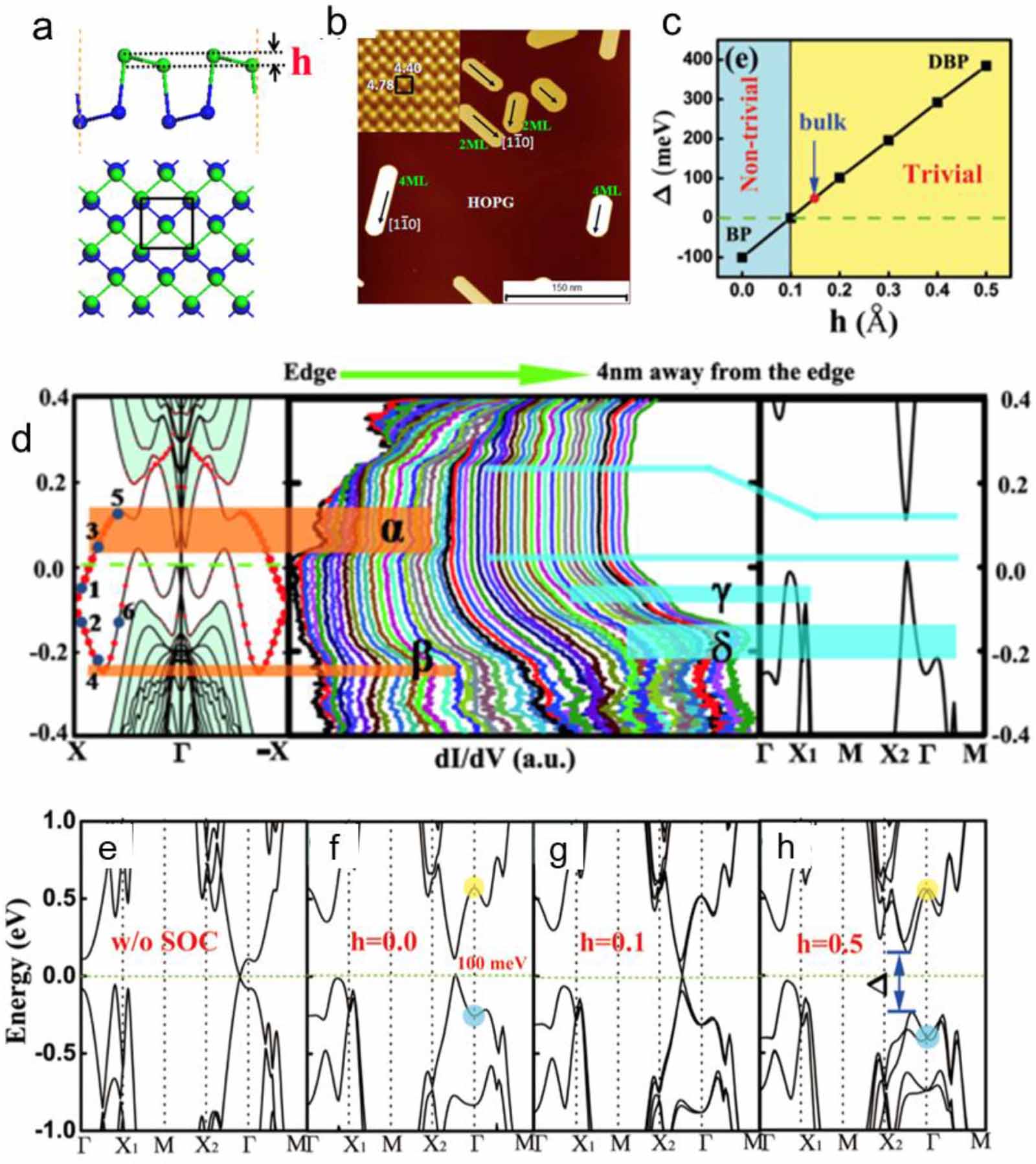
The freestanding Bi(110) layer adopts a puckered structure, as shown in figure 4(a), forming the distorted black phosphorus structure with variable h. Bi(110) thin films can be acquired by depositing Bi on highly oriented pyrolytic graphite (HOPG) or Si(111) substrate with less than four layers [17, 18]. Although a previous report implied a topologically trivial feature of Bi(110) thin film [19], the STM/STS experimental results combined with DFT calculations revealed that the buckling degree of the top two type-Bi atoms could modulate the topological properties of Bi(110) thin films from topological nontriviality to triviality [13]. A flattened Bi(110) with a thickness of two monolayers (MLs) and four MLs (figure 4(b)) can be obtained after depositing Bi atoms on the HOPG substrate, with h = 0 resembling the black phosphorus structure. Moreover, the relationship between the energy gap and the sublattice height difference h of the two ML Bi(110) films is calculated, where the energy gap is determined by the h (figure 4(c)). When h
 0.1
0.1  , the SOC-induced band inversion is identified, resulting in a nontrivial topology of Bi(110). The STS curves in figure 4(d) reveal the energy gap and the related TES. The energy gap closes at h = 0.1
  , where the topological phase transition (TPT) occurs. With a further increment in h, the energy gap reopens, and the band structure turns out to be a topological triviality (figures 4(e)–(h)). In experiments, the different values of sublattice height difference are expected to be controlled by the interface interactions between Bi(110) and different underlying substrates. Therefore, seeking suitable substrates to accommodate Bi(110) thin films is regarded as an effective way to modulate their topological properties.

Figure 4. (a) Side view and top view of the structure of Bi(110). h is the height difference between the top two atoms in the same monolayer. (b) STM image of two-ML and four-ML Bi(110) on the HOPG substrate. Inset shows the atomic resolution STM image of the Bi(110). (c) Calculated energy gap under different h of two ML Bi(110) layers. (d) Calculated band structure (left panel) and point STS measured from the edge to the terrace (middle panel). Right panel is the calculated band structure of infinite two ML Bi(110) layers. (e) Band structure of two ML Bi(100) layers with BP-structure without SOC. (f)–(h) Band structure of two ML Bi(110) layers with SOC under different buckling degrees. Reproduced with permission [13]. Copyright 2015, American Chemical Society.
Download figure:
Standard image High-resolution image2.3. Bismuthene on SiC
The interaction between 2D materials and underlying substrates is regarded as a useful means to change the crystalline structures and electronic features of 2D materials. Planar honeycomb bismuthene has been fabricated on a Si-terminated SiC(0001) substrate, as shown in figures 5(a)–(c), where the hybridization of pz -orbitals of Bi atoms with the bottom substrate is identified, pushing the pz -orbitals out of the low-energy region [14]. Consequently, the electrons near the Fermi level in bismuthene on SiC substrate are mainly contributed by px -orbitals and py -orbitals (figure 5(d)). In addition, their large on-site SOC directly determines the magnitude of the energy gap rather than the SOC between nearest neighbors of pz -orbitals under the second-order perturbation theory in the graphene case, leading to the formation of the largest topological nontrivial energy gap of 0.8 eV (figures 5(e)–(g)). A large bulk energy gap from −0.2 to 0.6 eV can be clearly seen in the line STS (figure 5(h)) collected at a position far away from the edge. As the tip approaches the edge, the DOS increases gradually, which means that it is a conductive 1D edge state. However, according to the theoretical prediction, the edge state is expected to have a linear dispersion relation that possesses a constant DOS under different energy levels. The point STS near the edge exhibits a pronounced dip near zero bias voltage, which is correlated to Tomonaga–Luttinger liquid (TLL) behavior. Stühler et al [20] carried out their experiments by measuring the edge states at different temperatures (from 10 to 100 K). The results are well fitted by using the TLL model (figure 5(i)). The TLL behavior can also be observed in other topological 1D edge channels [21], where the electrons are confined in a narrow space and the correlation between the electrons becomes remarkable. Consequently, the interaction between electrons is the origin of the suppression of low-energy tunneling.

Figure 5. (a) Schematic of the top and side view of bismuthene on SiC substrate. (b) and (c) Large-area and atomic resolution of bismuthene. (d) Calculated contribution of Bi s and p-orbitals to the band structure of Bi  -bands (without SOC). (e)–(g) Electronic structure of bismuthene without SOC (e), with SOC (f) and with the Rashba effect (g), respectively. (h) dI/dV curves measured at points marked in the inset of the topography. Reproduced with permission [14]. Copyright 2017, The American Association for the Advancement of Science. (i) Point STS acquired at the TES at different temperatures, and the data were fitted by the TLL model. Reproduced with permission [20]. Copyright 2020, Springer Nature.
Download figure:
Standard image High-resolution image3. Quasi-1D Bi4 X4 (X = I, Br)
3.1. Epitaxial growth of Bi4X4 nanoribbon
The most promising feature of QSHI is the 1D edge state, which can serve as a dissipative conducting channel and candidate for the applications of quantum computers. The building block of Bi4
X4 (X = I, Br) is 1D molecular chains stacking along the direction of both the c-axis and a-axis via van der Waals force (figure 6(a)). Based on the DFT results depicted in figures 6(b) and (c), the valence and conduction bands invert largely at the  point, causing the exchange of parity of the eigenstates. This results in the single-layer Bi4
X4(001) being a QSHI that possesses a large insulating gap of more than 200 meV, enabling the dissipative edge state to survive at room temperature [22]. Moreover, the atomically sharp conductive edge of Bi4
X4 nanoribbons along the chain direction provides an inherent advantage for the ideal 1D robust conducting channel. The quasi-1D Bi4I4 nanoribbons on Bi(111) films with the support of 6H-SiC substrate was successfully synthesized using the MBE method [23]. Figure 6(d) shows the STM topography of Bi4I4 nanoribbons with atomic resolution, and the straight edge without any distortion can be identified (figure 6(e)). The point STS curves at the 1D edge and the center of the terrace were carried out, as shown in figure 6(g), where a non-zero but gap-like black curve, with energy ranging from −200 to 160 meV and the 'V-shape' red curve, with finite DOS residing in the gap can be observed. The finite DOS is evoked by the TES. The STS mapping results (figure 6(f)) reveal a ∼1.5 nm width of the decaying length of the edge state, which is comparable to the decaying length of the TES observed in other QSHIs [14, 24–26]. Combined with first-principles calculations, the authors demonstrated that the observed edge state can be ascribed to the existence of the topologically nontrivial nature of Bi4I4(001) monolayer.
point, causing the exchange of parity of the eigenstates. This results in the single-layer Bi4
X4(001) being a QSHI that possesses a large insulating gap of more than 200 meV, enabling the dissipative edge state to survive at room temperature [22]. Moreover, the atomically sharp conductive edge of Bi4
X4 nanoribbons along the chain direction provides an inherent advantage for the ideal 1D robust conducting channel. The quasi-1D Bi4I4 nanoribbons on Bi(111) films with the support of 6H-SiC substrate was successfully synthesized using the MBE method [23]. Figure 6(d) shows the STM topography of Bi4I4 nanoribbons with atomic resolution, and the straight edge without any distortion can be identified (figure 6(e)). The point STS curves at the 1D edge and the center of the terrace were carried out, as shown in figure 6(g), where a non-zero but gap-like black curve, with energy ranging from −200 to 160 meV and the 'V-shape' red curve, with finite DOS residing in the gap can be observed. The finite DOS is evoked by the TES. The STS mapping results (figure 6(f)) reveal a ∼1.5 nm width of the decaying length of the edge state, which is comparable to the decaying length of the TES observed in other QSHIs [14, 24–26]. Combined with first-principles calculations, the authors demonstrated that the observed edge state can be ascribed to the existence of the topologically nontrivial nature of Bi4I4(001) monolayer.

Figure 6. (a) Crystal structure of Bi4Br4. Single-layer Bi4I4 and Bi4Br4 share the same structure as the top layer in (a). (b) Band inversion near the  point of single-layer free-standing Bi4I4. (c) Band structure of monolayer Bi4Br4 nanoribbon with a linear TES in the energy gap. (d) Atomically resolved STM image of Bi4I4(001) nanoribbon on the top of Bi(111) films with the support of a graphene/SiC substrate. (e) Topography of Bi4I4 (001) nanoribbon with several types of defects at the edge. (f) STS mapping acquired in (e) under bias voltage of 150 mV. (g) Point STS curves measured at the edge and terrace. Reproduced with permission [23]. Copyright 2021, American Chemical Society. (h) High-resolution STM image of Bi4Br4 (001) with a step edge. (i) STS mapping measured along the purple line in panel (e). Yellow and purple arrows are marked for the effective region of the TES. Reproduced with permission [27]. Copyright 2022, American Chemical Society.
Download figure:
Standard image High-resolution image3.2. Surface electronic structure of Bi4Br4 single crystal
Bulk Bi4 X4 can be treated as a self-supported substrate for monolayer Bi4 X4 due to the weak van der Waals interaction along the c-axis. Moreover, the weak interlayer interactions can preserve their intrinsic topological properties. The crystal structure and electronic properties of the cleaved (001) surface of Bi4Br4 single crystal have been studied using the STM and ARPES methods [27]. A large area of Bi4Br4(001) with a smooth surface was acquired on the bulk substrate by cleaving the single crystal. Atomical sharp edges are observed in figure 6(h), where the line STS along the direction perpendicular to the edge exhibits a large gap around 0.2 eV and the edge state residing in the gap energy region with a 1.7 nm decaying length, as shown in figure 6(i). The gap value and position are consistent with the ARPES results. Combined with first-principles calculations, the gap has been identified to be a quantum spin Hall gap with band inversion at the M point of the Brillouin zone (BZ), revealing the topological nontriviality of the edge state. With the increment in temperature, the chemical potential is shifted, leading to the Lifshitz transition and the Fermi level in the gap region at room temperature. It should be noted that the gap value shows a weak dependence with the change in temperature, preserving the quantum spin Hall gap of ∼0.2 eV and consequently promising the potential application of this material in electronic and spintronic devices to overcome thermal perturbations at room temperature. The temperature-dependent ARPES results are consistent with the temperature-dependent STS mapping results, where the TES survives at room temperature due to the large energy gap and atomically sharp edge [28].
4. WTI: Bi14Rh3I9
The WTIs, 3D allotropes of 2D QSHIs, can be formed by stacking 2D QSHIs along the out-of-plane direction with weak interlayer interactions [29]. Theoretically, WTIs possess even numbers of band inversions at different time-reversal invariant points. Consequently, topological surface states in a WTI emerge on a particular side surface, and the top surface of a WTI can be treated as a layer of QSHI. Bi-based WTIs, which have been supported by experiments, include  -Bi4I4 and Bi14Rh3I9. The former was verified by the ARPES experiments carried out by Noguchi et al [30]. We review the topological properties of Bi14Rh3I that have been explored using STM/STS methods.
Bi14Rh3I consists of two types of alternately stacked layers, i.e. [(Bi4 Rh)3I]2+ layer that was predicted to be a 2D TI and [Bi2I8]2− layer that serves as a trivial spacer (figure 7(b)) [31]. The STM image of the cleavage surface of Bi14Rh3I (figure 7(a)) exhibits two different layers that can be identified with different layer heights. The 2D TI layer exhibits a graphene-like honeycomb lattice, and the trivial spacer layer forms a hexagonal arrangement of iodide ions in STM images (figures 7(d) and (c)). There are several types of QSHIs, while their 3D allotropes are not concluded in WTI due to the existence of interlayer interaction even in a weak van der Waals force. However, the 2D TI layer in Bi14Rh3I is intercalated by the spacer of the trivial [Bi2I8]2− layer to further weaken the interlayer interaction. Moreover, the trivial layer exhibits a gap feature in the energy region of the quantum spin Hall gap and TES in the 2D TI layer, as shown in the STS curves in figure 7(f), resulting in there being no electronic states from trivial layer hybrids with the TES in 2D TI. The pronounced peak in the gray curve (figure 7(f)) indicates a TES of the 2D TI layer, and the STS mapping in figure 7(h) under a bias of −250 mV displays a DOS distribution in real space (figure 7(g)), where the robust TES distribution along the edge is artificially created by the atomic force microscope.

Figure 7. (a) Large-area STM image of the cleaved Bi14Rh3I9 surface. Inset is the height profile along the green line. (b) Schematic of Bi14Rh3I9 crystal structure. Red cells are [(Bi4 Rh)3I]2+ and the blue cells represent [Bi2I8]2−. Atomically resolved image of (c) [(Bi4 Rh)3I]2+ layers and (d) [Bi2I8]2− layers, respectively. (e) Step edge between [(Bi4 Rh)3I]2+ and [Bi2I8]2− layers. (f) Point STS measured at the points marked in panel (e). (g) STM image and (h) STS mapping of 2D TI layer. STS is taken under bias voltage of −250 mV. Reproduced with permission [31]. Copyright 2015, Springer Nature.
Download figure:
Standard image High-resolution image5. STI: Bi2Te3
The family of A2
B3 (A= Bi, Sb; B= Te, Se) topological materials in 3D STI has attracted intensive studies in recent decades [32–34]. The crystal structure of the A2
B3 family is shown in figure 8(a), where a quintuple layer with B–A–B'–A'–B'' is indicated by the red square. A single Dirac cone on the (001) surface can be found in the bulk insulating gap calculated by DFT (figure 8(b)) [35]. In contrast to WTI with partial surface states, STIs possess completely conductive topological surface states, where back-scattering is prohibited due to spin-momentum locking. Using the STM and STS methods, Zhang et al [36] investigated the STS mapping on Bi2Te3 and the corresponding scattering wave vector in momentum space, which provided convincing evidence for the lack of backscattering of electrons on the surface of a 3D TI. In their experiments, high-quality Bi2Te3 thin films were grown using the MBE method, and a few Ag trimmers were deposited on the top surface to serve as a non-magnetic scattering center (figures 8(d) and (e)). Figures 8(f)–(j) display various standing waves induced by four Ag trimmers on the Bi2Te3 top surface under different bias voltages. The fast Fourier transform (FFT) (figures 8(k)–(o)) of the dI/dV maps in figures 8(f)–(j) reflects the component of the scattered wave vector ( ). It is found that the wave vector in
  space mainly consists of only one direction, namely
  −
− . The results can be understood by investigating the constant-energy contour of the band structure of Bi2Te3. Figure 8(c) exhibits the three main kinds of possible scattering wave vectors in the reciprocal space, namely
  ,
,  and
and  . The scattering wave vector observed in experiments is
  , and the
  represents the back-scattering vector and, as a result, is prohibited.

Figure 8. (a) Crystal structure of Bi2Se3 family.Primitive cell is marked by black lines. (b) Band structure of Bi2Te3 from first-principles calculations. Reproduced with permission [35]. Copyright 2009, Springer Nature. (c) Constant energy contour of the band structure of the Bi2Te3(111) surface. Red arrows represent the possible initial and final vectors of the quasi-particle. (d) STM image of an area with four Ag trimmers adsorbed on the Bi2Te3(111) surface. (e) Adsorption site of Ag trimmer. (f)–(j) dI/dV mapping in the same area as (d) at different bias voltages. (k)–(o) Corresponding FFT power spectra of the dI/dV mapping in (f)–(j). Reproduced with permission [36]. Copyright 2009, American Physical Society.
Download figure:
Standard image High-resolution image6. HOTIs: bulk bismuth, α -Bi4Br4
HOTIs have been proposed as an extension of topological classification according to the Z4 topological index [37]. The bulk-boundary correspondence in second-order TIs is that a d-dimensional TI has a (d-2)-dimensional gapless boundary state. For instance, conductive channels emerge only on the 1D hinge of a 3D HOTI, while their bulk and surfaces maintain an insulating state. The high-order topology proposed in Bi-based materials was verified by experiments that include the bulk bismuth [8] and  -Bi4Br4 [38].
Bulk bismuth has been regarded as a topologically trivial material under the Z2 criterion before the notion of HOTI was proposed. Some experimental results indicate that the 1D conductive edge state survives in thick Bi(111) films and bulk bismuth, and its origin is explained as a TES of 2D QSHI [7, 39]. The STM/STS technique combined with theoretical calculations and transport measurements reveals the nontriviality of bulk bismuth. The conventional unit cell (red line) and primitive unit cell (black line) are shown in figure 9(a), which exhibit three-fold rotational ( 3) symmetry and spatial inversion symmetry. Theoretical analysis indicates that the bulk bismuth holds the conductive hinge states. These hinge modes are simultaneously protected by time-reversal symmetry,
  3 symmetry and spatial inversion symmetry. Figure 9(b) shows the band structure of the bismuth with inversion eigenvalues (green) and
  3 eigenvalues on the
  line (black). A hexagonal pit was found in an STM topography image, and the location of hinge models is drawn as purple lines. The red and blue arrows represent the spin-momentum locked flow. The differential conductance map in figure 9(d) exhibits a good agreement with figure 9(c) and supports the theoretical prediction that bulk bismuth is a HOTI.

Figure 9. (a) Conventional and primitive cell of bismuth. (b) Band structure of bulk bismuth and '±' marks the parity of the eigenstate at high-symmetry momentum points. (c) STM topography of a pot observed in experiments. (d) STS mapping measured in the same area in panel (c). Reproduced with permission [8]. Copyright 2018, Springer Nature.
Download figure:
Standard image High-resolution imageRecently,  -Bi4Br4 was theoretically predicted to be a HOTI, where the conductive channel emerges only on the hinge between the (001) surface and the (100) surface. Noguchi et al [38] reported an investigation on the topological properties of crystal
  -Bi4Br4 using their laser ARPES equipment. Due to the lack of spatial resolution for ARPES methods, the origin of the edge states observed in their experiments needs to be further confirmed by allying with other experimental techniques. Using the STM/STS methods with high spatial resolution, Shumiya et al [28] studied the DOS difference at the two kinds of edges due to the possible hybridization of edge states between two adjacent layers.
7. Dual topological material: Bi2TeI
Dual topological materials possess two classes of topologies. Recently, a few dual topological materials have been proposed and have been identified in experiments [40–42]. Bi2TeI was reported to exhibit dual topology with the properties of WTI and TCI on the top surface [43]. The crystal structure of Bi2TeI is shown in figure 10(a), in which a single Bi(111) bilayer is stacked in the middle of two layers of BiTeI. It has been revealed by experiments that the Bi(111) layer is a QSHI, as discussed above. Bi2TeI holds the properties of WTI due to the weak coupling between Bi(111) layers and the intercalated BiTeI layer, similar to the case of Bi14Rh3I. There are two Dirac cones located at the Z point and  point of the BZ, respectively. Both Dirac cones project to the cleavable surface with an energy deviation, which is expected to be hybridized with each other and opens an energy gap without the protection of symmetry. The mirror symmetry of the crystal leads to Bi2TeI, a TCI, and protects a degenerate nodal line at the intersection points, as shown in figure 10(c). The STM topography image of the cleaved surface of Bi2TeI is depicted in figure 10(d), where three kinds of surfaces are exposed. The LDOS (figure 10(f)) measured along the gray line in figure 10(d) shows metallic properties throughout the surface with partial suppression of DOS next to the step edges (figure 10(g)), which is caused by the opening of an energy gap of Dirac cones due to the mirror-symmetry breaking at the step edges. The WTI nature is demonstrated by the measured DOS at different edges. The topological 1D channel appears only at the edge of the terrace terminated by a bilayer Bi(111) (5–6, figure 10(j)) and the LDOS of the edges of two other types of edges (3–4, figure 10(h); 4–5, figure 10(i)) does not exhibit any increase in the in-gap energy.

Figure 10. (a) Schematic of the crystal structure of Bi2TeI. (b) Bi(111) bilayer in the bulk Bi2TeI and its TES in the energy bands. (c) Bulk band structure projected into the top surface of Bi2TeI is protected by crystal symmetry. (d) Cleaved surfaces of Bi2TeI obtained using STM. (e) Schematic of the exposed surfaces and steps corresponding to panel (d). (f) STS mapping measured along the gray line in panel (d). (g) Point STS curve acquired at the position marked by blue and black arrows in panel (f). Inset shows the gap opening due to the mirror-symmetry breaking near the step. (h)–(j) Point STS curves obtained at different positions marked in panel (e). Reproduced with permission [43]. Copyright 2020, Springer Nature.
Download figure:
Standard image High-resolution image8. Topological Dirac semi-metal (TDS) and TPT in Na3Bi
TDS, a counterpart of graphene in 3D form, has attracted significant interest in recent years [44–47]. The band structure of the 3D TDS can be regarded as a 3D Dirac cone in 4D space, and its projection to the 3D space can be attributed to a graphene-like 2D cone (figures 11(a)–(c)). Moreover, 3D TDS is a critical topological state similar to many other topological materials, such as Weyl semi-metal, trivial insulator, TI, axion insulator, etc. Na3Bi is predicted to be a 3D TDS, which has been verified by ARPES experiments [9]. The crystal structure of Na3Bi is shown in figure 11(d) with van der Waals interlayer interaction. Similar to graphene, the quasi-particle interference (QPI) phenomenon (figure 11(e)) has been observed [48] in the surface of Na3Bi by STS mapping under different energies, where an isotropic Fermi velocity in both directions perpendicular to the cleavage plane, which is expected for a 3D TDS, can be deduced.
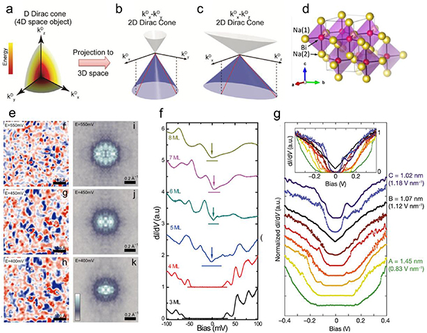
Figure 11. (a) 3D Dirac cone in TDS and the color represents the energy scale in the 3D BZ. (b) and (c) 2D Dirac cone in a plane from the projection to 3D space of the 3D Dirac cone in (a). Reproduced with permission [9]. Copyright 2014, The American Association for the Advancement of Science. (d) Crystal structure of Na3Bi. (e) STS mapping images acquired under different bias voltages and corresponding quasi-particle patterns. Reproduced with permission [48]. Licensed under a Creative Commons Attribution (CC BY) license. (f) Thickness-dependent differential spectra taken on the surface of different layers of Na3Bi. Reproduced with permission [49]. Copyright 2019, American Chemical Society. (g) Normalized STS measured on two ML Na3Bi at different tip electric field. Inset is the original data without offset, indicating a nonzero DOS in a conductive surface. Reproduced with permission [50]. Copyright 2018, Springer Nature.
Download figure:
Standard image High-resolution imageThe TPT can be induced by varying the thickness of Na3Bi films [49] or applying an external electric field to the ultrathin Na3Bi layers [50]. A transition from semi-metal to TI occurs when the thickness of Na3Bi films decreases from bulk to four layers or fewer (figure 11(f)). The topological nature of ultrathin Na3Bi films grown using the MBE method has also been modulated by the tip electric field. The strength of the electric field is controlled by doping potassium on the surface or approaching the STM tip. The gap closing and reopening can be clearly identified in the point STS curves (figure 11(g)) with the increase of tip electric field from 0.83−1.18 V nm−1, where the monolayer or bilayer Na3Bi experiences a TPT from nontriviality to triviality. The large insulating gap under a low electric field suggests a promising topological transistor for room-temperature applications in the future. The TPT induced by an electric field has special significance in applications due to the electric on-off being widely adopted in electrictronic devices, such as chips.
9. Magnetic topological materials: MnBi2−x Sbx Te4
The intrinsic magnetic topological insulator, MnBi2Te4, has attracted significant attention in recent years due to its coexisting inherent magnetic order and topologically nontrivial band structure [51]. Crucial quantum states, such as the quantum anomalous Hall effect, axion insulating state, Weyl semi-metal state, and other exotic states depending on the magnetic order configuration were observed in this material [52]. The structure of single-layer MnBi2Te4 is displayed in figure 12(a), which has septuple layers of Te–Bi–Te–Mn–Te–Bi–Te stacking order. The phase transition from antiferromagnetic (AFM) order to paramagnetic order occurs at 24.2 K (Neel temperature), and the AFM order comes from the oppositely aligned magnetic moment of interlaminar Mn layers. MnBi2Te4 is an STI in the system, implying that a surface state with Dirac cone dispersion can be seen on the (0001) surface. After the AFM order is turned on, a magnetic gap is opened at the Dirac point. Experimentally, the surface state was mainly investigated using the ARPES method in previous studies, where the gapped and gapless surface spectra were observed simultaneously, leading to an inconclusive value of the magnetic energy gap [53, 54].

Figure 12. (a) Atomic structure of single-layer MnBi2Te4. (b) STM image of MBST (x = 0.64) and inset shows the LEED image of the (0001) surface. (c) Point STS curves acquired on three MBST compounds with x = 0, x = 0.6 and x = 2, respectively. (d)–(f) Line cuts of QPI patterns on MBST compounds. Inset in panel (e) is acquired with the tip close to the surface, which shows a surface band gap of about 50 meV. Reproduced with permission [55]. Copyright 2020, American Physical Society.
Download figure:
Standard image High-resolution imageKo et al [55] reported band structure of MnBi2−x Sbx Te4 (MBST) measured using the STM/STS method with QPI patterns. The bulk MnBi2Te4 exhibits an electron-doped band structure, and the Fermi level is tuned into the bulk band gap by substituting Bi with Sb elements without changing the AFM order of the ground state. The atomic STM topography of the cleaved (0001) surface of MBST (x = 0.64) is shown in figure 12(b), in which many defects can be observed. The Fermi level moves from the conductive band (x = 0), residing in the bulk band gap (x = 0.64), to the valence band (x = 2), as shown in the point STS curves of three samples (figure 12(c)). The QPI images in figures 12(d)–(f) reflect the detailed evolution of the band structure in MBST samples. When x = 0, a topological surface state can be clearly seen in the bulk band gap. However, the magnetic gap is not large enough to be identified due to the strong background of bulk scattering wave vectors. As the Sb substitutes the Bi with x = 0.64, a magnetic gap of around 50 meV is formed in the topological surface state. In contrast, no surface state is found in the bulk band gap of the x = 2 compound, indicating a topologically trivial insulator for MnSb2Te4.
10. Conclusion
In this review, we provide a brief introduction to the development of Bi-based TQMs from the point of view of both theoretical simulations and experimental methods of the STM technique. Compared to other techniques, such as ARPES, STM is a powerful tool to identify topological electronic features at high spatial resolution, which is ideally applied to characterize the topological surface/edge states in TQMs. Furthermore, the tunneling current between the tip and sample can be used as an external factor to modulate the topological properties of these TQMs. The strong SOC provides a large energy to induce the band inversion, and consequently results in a large topological nontrivial gap. However, the highest temperature of the quantum spin Hall effect detected by transport experiments is 100 K [24], which is a long way from room temperature. There are three factors determining the survival temperature of the quantum spin Hall effect: a large energy gap to overcome the thermal perturbation, atomic sharp edges to minimize the scattering and a long coherent length to promise the electron interference. The STM results reveal that Bi4Br4 is QSHI with a large energy gap and atomic sharp edge, according to the first two factors to realize the high-temperature quantum spin Hall effect. Thus, transport measurements of high-quality monolayer Bi4Br4 are expected to solve this mystery.
It is noticeable that most of the Bi-based TQMs can be made up of four building blocks: Bi bilayer, Bi2(Se,Te)3, BiTeX (X = Cl, Br, I) and MBi2Te4 (M = Pb, Sn, Ge, Mn), as shown in figure 13(a) [56]. These and their 3D allotropes possess different topological properties, and their combinations reflect abundant topological features. The materials comprising Bi and Bi2(Se,Te)3 include BiSe, BiTe and Bi4Se3, which are composite WTI, WTI plus TCI and TSM, respectively (figure 13(b)) [40, 57, 58]. The group of Bi bilayers and BiTeX can be Bi2TeX, which is a composite WTI plus TCI [43, 59]. In addition, the topological properties of other compounds, Bi3TeX and Bi4Te3, remain inconclusive (figure 13(c)) [60, 61]. Bi2(Se,Te)3 can also intercalate into the MBi2Te4 layer to form MBi2+2x Te4+3x and weaken the interlayer magnetism interaction between the MBi2Te4 adjacent layers and to restore the intrinsic topological properties of monolayer MBi2Te4 (figure 13(d)) [62–65]. More groups of these building blocks are expected to be fabricated to realize novel topological properties. For example, the group of Bi bilayers and MBi2Te4 is expected to give rise to the quantum anomalous Hall effect due to the fact that the out-of-plane moment in MBi2Te4 can break the time-reversal symmetry in Bi bilayer (QSHI) to create a more robust one-branch edge state.

Figure 13. (a) Four building blocks that consist of a large family of the Bi-based TQMs. Blue solid (orange dash) arrows connecting two blocks represent the reported (unreported) compounds stacked by the two corresponding blocks. (b)–(d) Schematic of different stacking orders of the existing topological materials consisting of building blocks connected by a blue solid line in panel (a).
Download figure:
Standard image High-resolution image
Acknowledgments
This work is supported by the Beijing Municipal Natural Science Foundation (Grant No. Z180007), the National Natural Science Foundation of China (Grant Nos. 11874003, 11904015 and 52073006) and the Australian Research Council (ARC) (LP180100722).