

Abstract
Single crystal is the most advantageous of the crystalline states of halide perovskites. It displays better optical and electrical capabilities than polycrystalline films and microcrystals due to their inherent structural advantages, such as free grain boundaries, long-range ordered structure, and high orientation. Single-crystal perovskite materials can theoretically enable optoelectronic devices with higher performance and stronger stability. In this review, the intrinsic physical properties of perovskite single crystals are analyzed. The most recent advances in single-crystal optoelectronic devices are reviewed, and the design principles of the devices under different application conditions are revealed. It provides potential solutions for remaining challenges, and it is expected to accelerate the development of perovskite based optoelectronic devices.
Export citation and abstract BibTeX RIS

Original content from this work may be used under the terms of the Creative Commons Attribution 4.0 license. Any further distribution of this work must maintain attribution to the author(s) and the title of the work, journal citation and DOI.
1. Introduction
Recently, lead halide perovskites have been considered the most promising semiconductor material due to their superior optoelectronic properties, including a modifiable energy bandgap [1–3], long carrier diffusion lengths [4], a high absorption coefficient [5], and low cost [6, 7]. Hence, perovskite materials have been widely applied in the fabrication of optoelectronic devices, such as solar cells [8, 9], photodetectors [10–12], light-emitting diodes (LEDs) [13–15], and laser applications [16–18]. The chemical formation of perovskites can be represented by ABX3, where A is a monovalent cation (e.g., methylammonium MA+, formamidinium FA+, or Cs+), B is a divalent metal cation (e.g., Pb2+ or Sn2+), and X is a halide anion (I−, Br−, and Cl−). The first organic-inorganic hybrid perovskite, CH3NH3PbX3 (X=Cl, Br, and I), was synthesized in the early 1970s [19], although it did not attract much attention from researchers for the next century. In 2009, Japanese scientist Miyasaka used CH3NH3PbI3 and CH3NH3PbBr3 as a sensitizer for the first time in dye-sensitized solar cells [20], thus initiating a worldwide investigation of perovskite materials. Perovskite materials have achieved significant advances in the semiconductor photoelectron field after decades of research. Among them, single-crystal perovskites can most faithfully reveal the intrinsic physical and chemical properties of the material.
Due to the unique crystalline structure of single-crystal perovskites, they exhibit excellent optical and electric properties. First, lead halide perovskites are strong light-harvesting semiconductors with a direct bandgap. A material with a high absorption coefficient absorbs all light with energy above the bandgap, minimizing photon loss. Besides, the absorption edge of single-crystal perovskites exhibits distinct redshifts, which increases the range of light-harvesting materials. Second, lead halide perovskites have a low exciton-binding energy (EB), enabling efficient separation of light-generated Frenkel excitons. For example, previous studies have reported a wide range of values for the EB of MAPbI3, ranging from 2 meV to 75 meV [21–26]. The EB is similarly sensitive to the microstructure of perovskites. In polycrystalline films, the EB decreases due to electrostatic potential disorders, inhibiting the formation of excitons. Consequently, the strong excitonic peak of MAPbI3 can only be observed in the millimeter-sized single crystals. Finally, the low defect density of single-crystal perovskites ensures excellent carrier transport behavior. According to a previous study [4], the diffusion lengths of a MAPbI3 single crystals exceeding 175 μm are the longest among typical direct-bandgap semiconductors, and its carrier mobility can reach 150 cm2 V−1 s−1. Improved optical and electric properties promote the application of photoelectric conversion, particularly in light energy utilization and optical signal recognition. For instance, solar cells comprised of FA0.6MA0.4PbI3 single crystals achieved an efficiency of 22.8% [27]. MAPbBr3 single crystals as x-ray detectors produced sensitivity four times greater than commercial α-Se x-ray detectors [28, 29]. These studies demonstrated that single-crystal perovskites have great potential for photoelectric conversion applications. In addition to promoting the high performance, perovskite single crystals are also beneficial for the preparation of micro-nano optoelectronic devices, particularly in the areas of LEDs and photodetectors. Micro-nano optoelectronic devices mainly act as photodetectors and often appear in the form of arrays, which are composed of a large number of pixels. The homogeneity of pixel units is crucial for the performance of the integrated device. As the unit size of micro-nano optoelectronic devices has been reduced to a level comparable to or even smaller than the perovskite grain size, the disorderly distributed grain boundaries in polycrystalline films can adversely affect the uniformity and performance of ordered arrays. Moreover, the polycrystalline film layer exhibits uneven grain orientation, which also compromises the consistency of the device array and poses challenges to the device miniaturization. Furthermore, the inconsistency of the array may also result in 'weak points', which force the array to operate under more stringent external constraints such as voltage and temperature. Perovskite single crystals have excellent uniformity, non-grain boundary and low defects, thus possessing consistent optical and electronic properties. Pixel array devices based on perovskite single crystals can achieve consistent performance for each unit. Additionally, a lower defect concentration implies a higher dark state resistance, which is essential to reduce the shot noise of photodetector.
However, the current research on perovskites focuses on the formation mechanism of polycrystalline films and the application of related devices. Compared with the well-developed polycrystalline perovskite devices, single-crystal perovskites have superior semiconductor characteristics, but the progress of devices is still lagging behind. The material properties of perovskite single crystal are extremely important for expanding the application field, especially in the micro-nano photoelectric filed. Therefore, considering the gap between the performance and application of single-crystal devices and polycrystalline devices, it is necessary to summarize the preparation process, physical properties, and application design of single crystal devices in order to accelerate the development of perovskite single-crystal devices. Up to now, there are several reviews of perovskite single crystals and their optoelectronic applications [30–33]. However, these studies describe the growth technology and applications of single crystals, excluding the effect of perovskite single crystals' fundamental properties on their applications. Herein, this review discusses the intrinsic physical properties of perovskite single crystals and their application to optoelectronic areas. Then, the recent development of optoelectronic devices is summarized and discussed. Finally, the remaining challenges are identified. The future research directions are suggested with insightful perspectives. Figure 1 illustrates the role of the excellent physical properties of single crystals in advancing optoelectronic applications.

Figure 1. Schematically demonstrating the fundamental physical properties of single crystals affect the optoelectronic application. 'Solar cells'. Reproduced from [9]. CC BY-NC. 'Photodetectors' Reproduced from [11]. CC BY 4.0. 'LEDs' Reproduced from [15], with permission from Springer Nature. 'Lasers' Reprinted with permission from [18]. Copyright (2017) American Chemical Society. 'Efficient, stable, integrated and micro-nano optoelectronic devices' Reproduced from [12]. CC BY 4.0.
Download figure:
Standard image High-resolution image2. Fabrication of perovskite single crystals
Perovskite single crystals are usually prepared using solution-based methods. According to the different principles of crystallization, we divide the growth methods of single crystals into the following three types: temperature cooling crystallization [34, 35], inverse temperature crystallization [36–38], and antisolvent vapor-assisted crystallization [39]. The growth mechanisms are shown in figure 2(a).

Figure 2. The basic growth mechanisms of crystal singles. Solubility curve of MAPbI3 in hydroiodic acid solvent, and gamma-butyrolactone solvent, Reproduced from [34] with permission from the Royal Society of Chemistry. Reproduced from [36]. CC BY 4.0, schematic diagram of the anti-solvent vapor-assisted crystallization process. From [39]. Reprinted with permission from AAAS. (b) A schematic illustration for the ultrathin SC wafer preparation by geometry-controlled [43] John Wiley & Sons. [© 2016 John Wiley & Sons, Ltd.]. (c) Scheme for growth of perovskite SCTFs by a facile space-confined solution-processed strategy. Reprinted with permission from [45]. Copyright (2016) American Chemical Society.
Download figure:
Standard image High-resolution imageBased on the three methods mentioned above, additional growth methods have been developed, such as the cavitation-triggered asymmetrical crystallization (CTAC) strategy [40] and the low-temperature-gradient crystallization (LTGC) method [41]. However, the optoelectronic applications based on bulk perovskite single crystals have faced substantial challenges due to the severe charge losses produced by the excessive thickness and mass surface defects of the single crystals. Scientists have developed various methods to synthesize single crystals of the proper thickness, with a space-confined method being the most common one [42–44]. Liu et al developed a method for growing ultrathin single-crystalline perovskite wafers with controlled thickness and shape [43]. The thickness of the crystal wafer was controlled by confining the crystal growth within a very narrow space, as shown in figure 2(b). The thickness of the wafer was continuously tunable from 150 μm to 1440 μm. However, the 150 μm thickness of wafers still impair the effective carrier vertical transport in optoelectronics device. Chen et al reported a new method that part of the parallel substrates with a limited space are vertically dipped in the perovskite precursor solution, as shown in figure 2(c) [45]. The precursor solution could fill the entire space due to the capillary pressure. The vertical temperature gradient in the solution can trigger the perovskite crystallization. The MAPbBr3 perovskite was synthesized with a thickness of only 13 nm, but its lateral dimensions were limited to hundreds of micrometers. Therefore, developing ultrathin perovskite single-crystal with a large aspect ratio, larger lateral area and thinner thickness, is still a problem that needs to be solved. Space-confined method is usually combined with top-down method, which enables thin single crystals to grow tightly on conductive or transport layer substrates [46, 47]. For example, ultrathin perovskite crystals can be grown on ITO/Poly[bis(4-phenyl)(2,4,6-triMethylphenyl)aMine] (PTAA), serving as the photoactive layer of vertical-structure solar cells, where PTAA can act as the hole-transport layer. Other special growth methods, including vapor phase epitaxial growth [48] and surface tension-assisted growth [49], will be elaborated in detail in the following chapters combined with the application.
3. Physical property of perovskite single crystals
3.1. Light-harvesting
The efficient collection of photogenerated carriers in photoelectric devices necessitates using light-active materials with a high light-harvesting capacity. Halide perovskites, as direct-bandgap semiconductors, have ultraviolet (UV)-visible absorption coefficients as high as 105 cm−1 [50, 51], which is an order of magnitude greater than silicon. The optimal absorption bandgap of perovskite enables photoresponse across the visible spectrum (390–780 nm), which is beneficial for solar energy utilization and broadband detector applications (as shown in figure 3(a)). Moreover, compared to polycrystalline films, the single crystal displayed a redshift absorption edge [52], which broadens the photoresponse range and facilitates the collection of additional photons [53–55]. The redshift of the absorption is related to the indirect bandgap absorption transition. Previous studies have reported that the Rashba spin–orbit coupling gives rise to an indirect gap of perovskite, few tens of meV lower in energy than the direct one [53]. Generally speaking, indirect transitions are 3–4 orders of magnitude less efficient than direct ones at absorbing light in semiconductors [56]. Therefore, single crystals with micrometer thickness can show clearly indirect bandgap absorption except for direct bandgap absorption. Although perovskite single crystals have a broader light absorption spectrum, but to adapt to some optoelectronic applications, such as infrared (IR) light detection, the light absorption range of perovskite materials needs to be further enlarged. Some studies have shown that the light absorption performance of perovskite can be tuned by deliberately introducing defects. For example, by introducing deep level defect states into perovskite, absorption of photons with sub-bandgap or below-bandgap energies can be achieved [57].
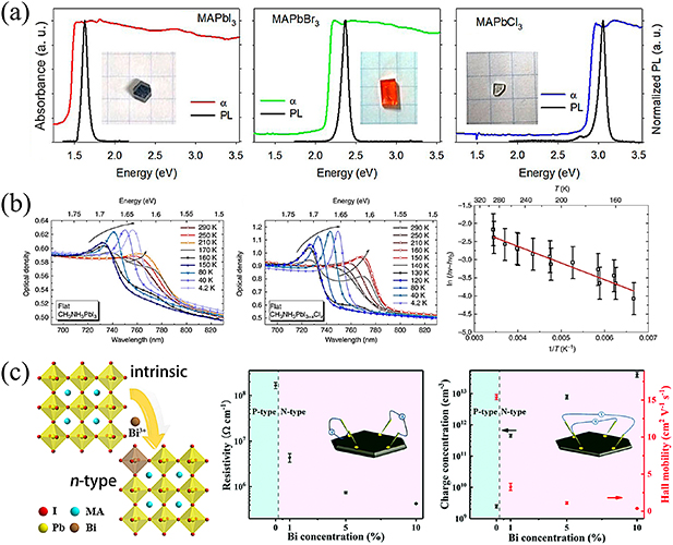
Figure 3. (a) The optical image, normalized absorbance and PL spectra of MAPbI3, MAPbBr3, and MAPbCl3, showing the band gap at room temperature. Reprinted with permission from [50]. Copyright (2017) American Chemical Society. (b) The absorption spectra of MAPbI3 and MAPbI3 − x Clx as temperature decreased (290–4.2 K), and corresponded fitting the data of EB. Reproduced from [23]. CC BY 4.0. (c) The resistivity (ρ), charge concentration (n) and Hall mobility (μH) change rule of MAPbI3 single crystals with Bi3+ doped. Reproduced from [26] with permission from the Royal Society of Chemistry.
Download figure:
Standard image High-resolution imageIn addition, by regulating the chemical composition, the photoresponse spectrum of a single crystal can be continuously tuned over a wide range of wavelengths. The bandgap of perovskites with the ABX3 structural formula can be modified by changing any site element. Considering the MAPbI3 single crystal, for instance, A-site MA+ can be replaced by a larger formamidinium ion (FA+), which shrinks the bandgap from 1.6 to approximately 1.48 eV [2, 38]. Similarly, substituting Pb2+ with Sn2+ at the B site yields a bandgap of 1.15 eV for MASnI3 [3]. Substituting I− of MAPbI3 with Br− and Cl−, the bandgap might expand to 2.24 and 2.97 eV, respectively [37]. In recent years, scientists have developed some growth methods for mixed composition crystals [58, 59]. A summary of the optical parameters of perovskite single crystals reported recently is presented in table 1 [27, 32, 60–76].
Table 1. The optical parameters of perovskite single crystals reported in the literature.
| The optical absorption edge (nm) | PL emission peak (nm) | The bandgap (eV) | ||
|---|---|---|---|---|
| MAPbCl3 | 435 | 440 | 2.88 | [60] |
| Cs2AgInCl6 | 384 | 595 | 3.2 | [61] |
| (PEA)2PbBr4 | 428 | 412 | 2.91 | [62] |
| CsPbCl3 | — | 412 | 3.01 | [63] |
| BA2PbBr4 | 400 | 411 | 3.1 | [64] |
| PMA2PbCl4 | 340 | 350 | 3.63 | [65] |
| MAPbBr3 | 553 | 545 | 2.24 | [66] |
| MAPbBr3 | 566 | 535 | 2.19 | [67] |
| CsPbBr3 | 561 | 556 | 2.21 | [68] |
| MAPbI3 | 850 | 781 | 1.45 | [69] |
| (FAPbI3)0.85(MAPbBr3)0.15 | 825 | 775 | 1.50 | [70] |
| Cs3Bi2I9 | 550 | 654 | 2.12 | [71] |
| Cs2AgBiBr6 | 625 | 550 | 1.98 | [72] |
| MAPb0.5Sn0.5I3 | 950 | — | 1.3 | [73] |
| Cs3Bi2I9 | 660 | 660 | 1.89 | [74] |
| FA0.6MA0.4PbI3 | 850 | 805 | 1.49 | [27] |
| FAPbI3 | 870 | 812 | 1.49 | [32] |
| DABCO-NH4Br3 | 250 | — | 5.25 | [75] |
| MDABCO-NH4I3 | 263 | 609 | 4.95 | [76] |
3.2. Charge transport behavior
3.2.1. Efficient free-charge-carrier generation.
The charge-carrier dissociation of charge carriers is mainly determined by the EB. For photovoltaic and photodetection applications, a small EB is preferable to minimize energy loss. The EB value for the typical perovskite MAPbI3 varies widely, with reported values ranging from 2 to 75 meV [22, 23, 77, 78]. Optical spectroscopy is a simple and convenient method to measure EB. As shown in figure 3(b), analyzing optical absorption, Snaith et al estimated the EB to be in the range of 55 meV for the mixed halide crystal MAPbI3 − x
Clx
[23]. Li et al determined the EB of the MAPbx
Bi1 − x
I3 single crystal to be ∼10 meV (10 K–150 K) using the temperature dependency of photoluminescence [26]. In addition, Miyata et al proposed that a high magnetic field spectroscopic analysis directly establishes more accurate EB without the dielectric constant ( ) assumption. This technique estimated the EB of MAPbI3 to be just 16 meV at 2 K [78]. These results indicate that halide perovskites are considered a nonexcitonic material, in which excitons dissociate into free charges following illumination, resulting in a photovoltaic effect. However, not all perovskite single crystals have small EB. The different structures determine different values of EB in perovskite single crystals.
The dimensionality of the crystal structure has a considerable impact on the EB. The two-dimensional (2D) perovskite materials (A2A'n − 1Mn X3n + 1) show a much larger EB than three-dimensional (3D) materials under quantum and dielectric confinement [79–82]. For instance, the EB values of 380 meV and 270 meV have been reported for (BA)2(MA)n − 1Pbn I3n + 1 with n = 1 and 2, respectively [81]. Using low-temperature optical spectroscopy, Blancon et al experimentally determined the EB drop from 470 meV to 125 meV in the (BA)2(MA)n − 1Pbn I3n + 1, with n varying from 1 to 5 [79]. The 2D perovskites have larger EB, which does not hinder their efficient transport of carriers. A recent study revealed an internal exciton dissociation mechanism in (PEA)2(MA)n − 1Pbn I3n + 1 (n = 2 − 4) that can convert over 80% of excitons into free carriers in an ultrafast time scale (<1.4 ps) [83]. This provided a reasonable explanation for the excellent performance of 2D perovskites in photoelectric devices.
Moreover, the EB in perovskites is sensitive to morphology and crystallinity. Grancini et al found that the electron-hole pair interactions are easily influenced by the microstructure of the perovskite [84]. Combining optical spectroscopy and multiscale modeling, they proved that structural disorder and electrostatic potential changes could prevent exciton production in polycrystalline films. This demonstrated that the significant excitonic characteristics of perovskite can only be observed in large single crystals. Recently, using spectrally resolved transient absorption microscopy, the spatial distribution of the exciton in a single-crystal perovskite grain has been directly observed [85]. The results indicated that exciton was more likely to be formed in regions with higher crystallinity, whereas free carriers predominated in the small domain region of the grain.
3.2.2. Mobility, carrier lifetime, and diffusion length.
Carrier mobility (μ), lifetime (τ), and diffusion length (LD) were critical factors for carrier dynamics, with the diffusion length being defined by both the carrier mobility and lifetime. These basic carrier parameters of halide perovskite single crystals, as reported in the literature, are listed in table 2 [4, 39, 60, 86–89].
Table 2. The key optoelectronic parameters of perovskite single crystals reported in the literature.
| Materials | Mobility (cm2 V−1 s−1) | Carrier lifetime (ns) | Diffusion length (μm) | Trap density (cm−3) | Carrier concentration (cm−3) | References |
|---|---|---|---|---|---|---|
| MAPbCl3 (ITC) | For hole: 42 ± 9 (SCLC) | τs = 83 | 3.0–8.5 | For hole: 3.1 × 10¹⁰ (SCLC) | 4 × 10⁹ | [60] |
| τb = 662 (TA) | ||||||
| MAPbBr3 (ITC) | For hole: 60 (SCLC and Hall effect) | 242 | A few micrometers | For hole: 1.6 × 10¹¹ (SCLC) | For hole: 1011 (Hall effect) | [86] |
| MAPbBr3 (AVC) | 115 (ToF) 20–60 (Hall effect) 38 ± 5 (SCLC) | τs = 74 ± 5 τb = 978 ± 22 (TA) τs = 41 ± 2 τb = 357 ± 11 (TRPL) | 3–17 | (5.80 ± 0.6) × 109 (SCLC) | For hole: 5 × 10⁹ 5 × 10¹⁰ (Hall effect) | [39] |
| MAPbBr3 (ITC) | For hole: 24.0 ± 0.3 (SCLC) | τs = 28 ± 5 τb = 300 ± 26 (TA) | 1.3–4.3 | For hole: (3 ± 0.3) × 1010 (SCLC) | — | [87] |
| MAPbI3 (AVC) | 2.5 (SCLC) | τs = 22 ± 6 τb = 1032 ± 150 (TRPL) | 2–8 | (3.3 ± 0.3) × 1010 (SCLC) | 2 × 10¹⁰ | [39] |
| MAPbI3 (ITC) | For hole: 67.2 ± 7.3 (SCLC) | τs = 18 ± 6 τb = 570 ± 69 (TA) | 1.8–10.0 | For hole: (1.4 ± 0.2) × 1010 (SCLC) | — | [87] |
| MAPbI3 (TSSG) | For hole: 105 ± 35 (Hall effect); 164 ± 25 (SCLC) For electron: 24.8 ± 4.1 (SCLC); 24.0 ± 6.8 (ToF) | Under 1 sun: 8.2 × 10⁴ (TPV) 9.5 × 10⁴ (IS) Under 0.1 sun: 2.3 × 10⁵ (TPV) 2.0 × 10⁵ (IS) | For hole: 175 ± 25 | For hole: 3.6 × 10¹⁰ | For hole: (9 ± 2) × 109 (Hall effect) | [4] |
| For electron: 4.5 × 10¹⁰ (SCLC) | ||||||
| MAPbI3 | 68 (SCLC) | τs = 94 τb = 493 (TRPL) | 4.0 | — | — | [88] |
| α-FAPbI3 (ITC) | 4.4 (SCLC) 1.07 ± 0.25 (ToF) | τs = 32 τb = 484 (TRPL) | 0.5–2.2 | 6.2 × 10¹¹ (SCLC) | 1.5 × 10¹¹ | [89] |
| FAPbI3 | 41 (SCLC) | τs = 79 τb = 1393 (TRPL) | 2.9 | — | — | [88] |
Disordered grain boundaries in perovskite polycrystalline films hinder the carriers when transporting from grain to grain and directly affect carrier transport. Researchers have proposed some strategies to improve carrier transport conditions, such as increasing grain size using chlorine doping and controlling grain orientation [90]. perovskite single crystals are free of grain boundaries, contributing to the barrier-free transport of carriers. Meanwhile, charge transport can be affected by defects in perovskites. Under a built-in electric field, free charge carriers move toward the poles within the perovskite layer. However, their trajectories change under Coulomb forces when they encounter scatterers such as phonons and defects, affecting the transport efficiency. Defects in polycrystalline films are concentrated on surfaces and grain boundaries. In a perovskite single crystal without grain boundaries, there are fewer defects. The trap density of the perovskite single crystal (MAPbI3) was ∼1010 cm−3, which is 6−7 orders lower than that of the polycrystalline film with the same chemical composition [91]. Thus, the perovskite single crystal holds promise for efficient carrier transport.
Carrier mobility measures the rate of movement of carriers in semiconductors. The greater the mobility value, the quicker the carrier's transport. Time of flight (ToF), Hall effect, and space charge limited current (SCLC) are the most prevalent mobility testing technologies [39, 86, 87]. Yet, even for identical samples, mobility will vary depending on the measurement procedure. For example, the ToF and SCLC methods are sensitive to traps within bulk materials, but the impacts of surface defects may be insignificant. With a hole mobility of 164 cm2 V−1 s−1, the MAPbI3 single crystal has the highest carrier mobility known to date [4]. Carrier lifetime is the average time photogenerated carriers exist before recombination. MAPbI3 single crystals attain an extraordinarily extended carrier lifetime due to the absence of grain boundaries.
Long carrier lifetime and high carrier mobility determine the perovskite single crystal's long carrier diffusion distance, which is significant for optoelectronic devices. Specifically for solar cells and self-powered photodetectors, a long carrier diffusion distance is advantageous for minimizing carrier loss during the diffusion process, hence enhancing the quantum efficiency of devices [92, 93]. The longest reported carrier diffusion length exceeds 175 μm, which is several times greater than the absorption depth, allowing single crystals to become ideal materials for optoelectronic devices.
The carrier transport is also influenced by the internal electric field distribution in optoelectronic devices. Ideally, it depends on the energies of band edges and the intentional carrier doping level in the functional layers. Some studies propose to intentionally dope impurities into the perovskite lattice to tune the electron and hole concentrations and achieve the desired band structure. As shown in figure 3(c), Cao et al grew bismuth-doped CH3NH3PbI3 single crystals with Bi3+ by partially replacing Pb2+. The Hall test results demonstrated that doping with Bi3+ ions converted p-type to n-type electric conduction and increased the concentration of hole carriers by four orders of magnitude [26]. However, defects of the perovskite bulk or surface, which are often a form of unintentional doping, disrupt the ideal band arrangement between functional layers and influence the electric field distribution inside the optoelectronic device in an uncontrolled way. In contrast to polycrystalline films, perovskite single crystal has no grain boundary and fewer defects, which endow it with faster carrier mobility and longer carrier lifetime. Most single crystals are grown by the solution method, which causes the precursor solution erosion and the organic ammonium salts escaping on the surface, leading to surface damage and defect formation. The single crystal surface has more defects than the bulk. Surface defects can cause nonradiative recombination and mismatched energy level at the interface of optoelectronic devices. Finding suitable materials and growth method to repair and passivate the surface defects is the focus of future research on single-crystal defects. For example, Osman et al reduced the crystallization temperature of MAPbI3 single crystal in the ITC to avoid the loss of methylammonium iodide, yielding better quality single crystal with lower defects [94].
4. Solar cells based on perovskite single crystals
In light of the superior optical and electrical properties of the perovskite materials mentioned above, their application in photoelectric conversion has become widespread. The most prominent are solar cells. Solar cells are devices that convert photon energy into electrical energy and have stringent energy efficiency requirements. Even with a large number of grain boundaries, the power conversion efficiency (PCE) of polycrystalline based single-junction perovskite solar cells (PSCs) has achieved a certified value of 26%, catching up to the efficiency of commercial single-crystal silicon solar cells [95]. The perovskite single crystal is superior to polycrystalline films in all optical and electrical properties, demonstrating that single-crystal solar cells should be more efficient and stable. Based on this expectation, single-crystal PSCs were proposed, and great progress was made in this field. According to the device structure of perovskite single-crystal photovoltaic cells, they can be divided into the following two categories.
Most PSCs adopt a vertical sandwiched structure in which the perovskite light-absorbing layer is sandwiched between multiple additional functional layers (as shown in figure 4(a)) [27, 52, 96]. Most perovskite single crystals have a thickness on the millimeter scale. Yet, the thickness is considerably greater than the perovskite carrier diffusion length (∼175 μm), severely limiting carrier transport [4]. For developing vertically structured PSCs, it is crucial to fabricate thin single crystals of the appropriate thickness.

Figure 4. (a) Vertical and (b) lateral device structure of the single-crystal solar cells. Reproduced from [52]. CC BY 4.0. Reproduced from [97]. CC BY 4.0. (c) The mechanism of CTAC method to grow MAPbBr3 thin single crystals, and (d) the structure and EQE curves of devices [40]. John Wiley & Sons. [© 2016 John Wiley & Sons, Ltd.].
Download figure:
Standard image High-resolution imageAnother structure of PSCs is lateral single-crystal solar cells (as shown in figure 4(b)) [97]. The electrode shape and spacing in lateral devices can be controlled flexibly by fabricating the metal electrode on one side of the single crystal. This can lower the single-crystal thickness needed for easy device fabrication. It is believed that the interface between the electrode and perovskites contributes to the performance of lateral PSCs. According to the above two structural classifications, we shall discuss the development of perovskite single-crystal solar cells in detail.
4.1. Vertical-structured solar cells
As depicted in figure 4(c), Osman et al grew a 4 μm MAPbBr3 single crystal using a new single-crystal growth method based on CTAC in 2016. This first-of-its-kind fabrication of a single-crystal solar cell using an ITO/MAPbBr3/Au structure yielded an ultra-stable PCE of 5.11%. Furthermore, the TiO2 film as an electron-transporting layer was inserted between the ITO and MAPbBr3 layers. The devices achieved higher electronic extraction efficiency and a PCE of 6.5% (figure 4(d)). Subsequently, Kuang et al investigated the effects of the hole-transporting layer (HTL) on the performance of MAPbBr3 single-crystal solar cells [98]. The introduction of HTL greatly improves the efficiency of carrier transport in crystal solar cells. As shown in figure 5(a), using Spiro-OMeTAD as the HTL to fabricate FTO/TiO2/perovskite/HTM/Au solar cells resulted in a PCE of 7.11% compared to devices without a transporting layer (PCE = 1.98%). In 2018, Zhu et al employed Ostwald ripening-assisted photolithography (ORAP) to fabricate the MAPbBr3 single-crystal microarrays [99]. In addition, the solar cell devices were built with the structure FTO/TiO2/MAPbBr3 arrays/CH3-(CH2)17SiCl3 blocking layer/Spiro-OMeTAD/Au (figure 5(b)). The devices exhibited a PCE of 7.84%, confirming that the ORAP method is an effective way to manufacture PSCs. The bromide-based perovskites have a large bandgap (∼2 eV) and can only absorb light between 300 nm and 520 nm. As light-absorbing layers, it is necessary to produce perovskite materials with a narrower bandgap to broaden the sunlight absorption range and improve the utilization of the solar energy of the devices.
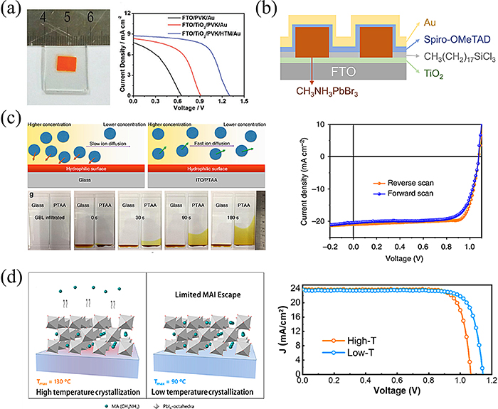
Figure 5. (a) The optical image of MAPbBr3 single crystals and the J-V curves of the MAPbBr3 single-crystal solar cells with different structures. Reproduced from [98] with permission from the Royal Society of Chemistry. (b) The structure of solar cell based on patterned MAPbBr3 single-crystal microarray. Reprinted with permission from [99]. Copyright (2018) American Chemical Society. (c) Growth mechanism and J-V characterization of MAPbI3 thin single crystal by space-limited inverse temperature crystallization. Reproduced from [52]. CC BY 4.0. (d) The growth schematic and solar cell performance of the MAPbI3 single crystal grown at high-temperature and low-temperature. Reprinted with permission from [94]. Copyright (2020) American Chemical Society.
Download figure:
Standard image High-resolution imageIn 2017, Chen et al developed a hydrophobic interface-confined lateral crystal growth method [52]. As shown in figure 5(c), micron-thick MAPbI3 single crystals were generated by a microflowing precursor solution over a hydrophobic layer to refill the solute for the single-crystal growth process. Using a 10 μm thick single crystal, they fabricated cells with the structure ITO/PTAA/MAPbI3/PCBM/C60/BCP/Cu. Through surface charge trap passivation, the best device had a PCE of 17.8% with a Jsc of 21.0 mA cm−2, a Voc of 1.08 V, and a fill factor (FF) of 78.6%. Perovskite's iodine was rapidly oxidized in the air. In subsequent research, all preparatory steps, including single-crystal growth, device fabrication, and characterization, were conducted in a nitrogen-filled atmosphere [100]. This prevented the oxidation of iodide ions in the precursor solution due to an increase in temperature. Hence, the devices achieved a PCE of 21.09% and an FF of 84.3%. Bakr et al found that using the ITC method to grow MAPbI3 single crystals requires a high growth temperature (>120 °C), which degrades the crystalline quality, particularly at the surface, because of methylammonium iodide (MAI) volatiles at such a high temperature [94]. Hence, they used a mixture of propylene carbonate and GBL as a solvent to lower the crystallization temperature (<90 °C) of MAPbI3. MAPbI3 single crystals of a higher quality and longer carrier lifetime were fabricated using a low-temperature crystallization technique. As shown in figure 5(d), the devices fabricated using a low-temperature strategy showed an increased Voc of up to 1.15 V and a leading PCE of 21.93%. Cationic and halogen vacancies generate most shallow-level defects in single-crystal solar cells. Li et al incorporated poly(3-hexylthiophene) (P3HT) into poly(triaryl amine) (PTAA) to interact with undercoordinated Pb2+ [101]. The x-ray photoelectron spectroscopy spectra of S 2p and Pb 4f of MAPbI3 single crystals in figure 6(a) indicate that P3HT coordinates with MAPbI3 single crystals. The incorporation of P3HT led to a reduction in defect density and the suppression of nonradiative recombination. In addition, the MAPbI3 single-crystal solar cells attained an ultrahigh efficiency of 22.1%, the highest value for MAPbI3 single-crystal solar cells. Narrowing the bandgap of perovskite materials closer to the optimal bandgap range (1.1–1.4 eV) for single-junction solar cells is an effective method to improve the PCE of solar cells. Due to its excellent bandgap of 1.4 eV, FAPbI3 perovskite materials are widely used in record-breaking polycrystalline solar cells [95]. In 2018, Zhou et al grew a mixed perovskite (FAPbI3)0.85(MAPbBr3)0.15 single crystal as solar cell absorbers for the first time [70]. According to the absorption spectra (figure 6(b)), the bandgap of the (FAPbI3)0.85(MAPbBr3)0.15 single crystal was close to 1.50 eV. As the absorption edge widened, the inverted device with the structure ITO/NiOx /(FAPbI3)0.85(MAPbBr3)0.15/TiO2/Ag exhibited a high Jsc of 23.14 mA cm−2. However, the PCE of solar cells was only 12.18% due to the immaturity of crystal growth technology. In 2021, a high-quality, mixed-cation single crystal (FA0.6MA0.4PbI3) was grown on PTAA using the ITC method [27]. Figure 6(c) demonstrates that the FA0.6MA0.4PbI3 single crystal exhibited a near-optimal bandgap (∼1.48 eV) and effectively redshifted the external quantum efficiency (EQE) band edge, making it approximately 50 nm longer than MAPbI3 single crystals. The devices may achieve ultrahigh Jsc values of over 26 mA cm−2 and PCEs of up to 22.8% without compromising Voc.
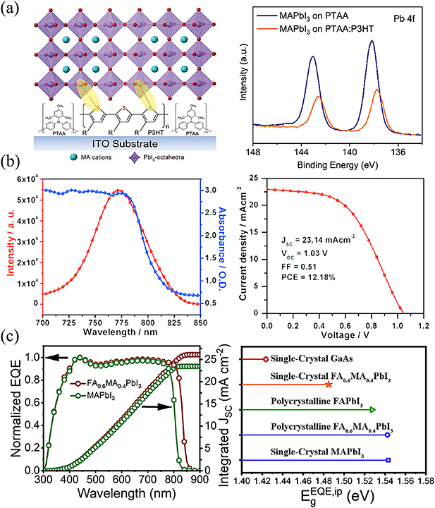
Figure 6. (a) Schematic illustration, and XPS proof of the interaction between P3HT molecule and perovskite single crystals [101]. John Wiley & Sons. [© 2022 John Wiley & Sons, Ltd.]. (b) The absorption and PL spectra of (FAPbI3)0.85(MAPbBr3)0.15 single crystals. The J-V curve of the best devices with the structure of ITO/NiOx /(FAPbI3)0.85(MAPbBr3)0.15/TiO2/Ag [70]. John Wiley & Sons. [© 2018 John Wiley & Sons, Ltd.]. (c) The bandgap value and EQE spectral comparison between different perovskite materials. Reproduced from [27] with permission from the Royal Society of Chemistry.
Download figure:
Standard image High-resolution imageIn 2019, Chen et al described a new differential space-limited crystallization method for synthesizing microthickness perovskite single crystals [102]. They created an asymmetric space for crystal growth using two sets of polytetrafluoroethylene spacers and placed a hydrophobic layer (VB-FNPD) within the micrometer-sized gap, further narrowing the gap. The best devices, based on the structure of ITO/VB-FNPD/MA0.75FA0.25PbI3/PCBM/Ag, exhibited a maximum PCE of 12.72%. The AVC growth method can be combined with a space confinement strategy for microthickness single-crystal growth. Using the AVC growth method, Guo et al grew MAPbI3 single crystals with tunable thicknesses ranging from a few hundred nanometers to several micrometers [103]. The AVC-fabricated solar cell-based single crystals exhibited a PCE of 20.1% with a Jsc of 22.6 mA cm−2, Voc of 1.08 V, and FF of 82.5%. In summary, the thickness of the single crystal has been controlled by the space-confined single crystal growth method; the quality of the single crystal has been improved by ligand engineering and crystallization process optimization; the carrier transport has been improved by the passivation of the functional layer interface. These are crucial to boost the efficiency of vertical single crystal PSCs, as shown in table 3 [27, 40, 52, 70, 94, 98–108].
Table 3. Summary of parameters of vertically structured single-crystal solar cells.
| Materials | Device structure | PCE (%) | Jsc (mA cm−2) | Voc (V) | FF (%) | References |
|---|---|---|---|---|---|---|
| MAPbBr3 | FTO/TiO2/perovskite/Au | 6.53 | 6.96 | 1.36 | 0.69 | [40] |
| MAPbBr3 | FTO/TiO2/perovskite/HTM/Au | 7.11 | 8.77 | 1.31 | 0.62 | [98] |
| MAPbI3 (ITC) | ITO/PTAA/MAPbI3/PCBM/C60/BCP/Cu | 17.8 | 21.0 | 1.08 | 78.6 | [52] |
| MAPbI3 | FTO/TiO2/MAPbI3/Spiro-OMeTAD/Ag | 8.78 | 22.28 | 0.668 | 0.59 | [104] |
| MAPbI3 | Au/ITO/Spiro-OMeTAD/perovskite-wafer/PCBM/LiF/Ag/Au | — | 20.02 | 1.15 | — | [105] |
| MAPbI3 | ITO/PEDOT/perovskite/PCVM/Ag | 4.4 | 22.15 | 0.75 | 0.27 | [106] |
| (FAPbI3)0.85 (MAPbBr3)0.15 | ITO/NiOx /perovskite/TiO2/Ag | 12.2 | 23.14 | 1.03 | 0.51 | [70] |
| MAPbBr3 | FTO/TiO2/perovskite/Spiro-OMeTAD/Au | 7.84 | 9.79 | 1.04 | 0.77 | [99] |
| MAPbBr3 | Au/perovskite/FTO | 2.3 | — | — | — | [107] |
| MAPbI3 (ITC) | ITO/PTAA/perovskite/C60/BCP/Cu | 21.1 | 23.46 | 1.076 | 83.5 | [100] |
| MA0.75FA0.25PbI3 | ITO/VB-FNPD/perovskite/PCBM/Ag | 12.7 | 22.99 | 0.89 | 0.62 | [102] |
| MAPbI3 (ITC) | ITO/PTAA/perovskite/C60/BCP/Cu | 21.9 | 23.68 | 1.15 | 81 | [94] |
| MAPbI3 (AVC) | ITO/PEDOT:PSS/perovskite/PCBM/BCP/Ag | 20.1 | 22.6 | 1.08 | 82.5 | [103] |
| FA0.6MA0.4PbI3(ITC) | ITO/PTAA/perovskite/C60/BCP/Cu | 22.8 | 26.2 | 1.1 | 79 | [27] |
| MAPbI3 (ITC) | ITO/PTAA + P3HT/perovskite/C60/BCP/Cu | 22.1 | 23.88 | 1.13 | 81.8 | [101] |
| MAPbI3-(100) (ITC) | ITO/PTAA/perovskite/PCBM/C60/BCP/Cu | 19.3 | 23.8 | 1.04 | 78.0 | [108] |
As summarized in table 3, single crystal PSCs show a significant performance gap compared with advanced polycrystalline PSCs, even though they having a high-quality perovskite absorption layer. Due to the complexity and lengthiness of preparing single crystal PSC, researchers tend to develop polycrystalline devices that can be fabricated by simple spin coating and electrode evaporation. Single-crystal PSCs still lag behind polycrystalline solar cells in aspects such as perovskite layer thickness control, surface defect passivation, functional layer interface modification, and electrode material optimization et al. In addition, some fabrication processing involving solution immersion may also cause additional damage of function layers, such as perovskite crystal growth based on PTAA/ITO substrate. By directly building lateral-structure devices on the crystal surface, these issues related to preparation and thickness control can be avoided.
4.2. Lateral-structured solar cells
In 2016, the Huang group was the first to fabricate lateral-structured devices with a simple Au/MAPbI3/Au structure by evaporating two parallel electrodes onto a bulk MAPbI3 single crystal [109]. They used a nonuniform field to polarize single crystals. After being polarized, the crystal-generated ion migration routes through the piezoelectric effect, forming p-i-n or n-i-p structures in the devices (figure 7(a)). The fabricated lateral-structured cells exhibited a low PCE of 1.88% under 0.4 sun illumination because of the crystal damage in the polarization process. In 2019, the group reported a bottom-up technique that allows the growth of centimeter-sized MAPbI3 crystal wafers directly from the surface of an aqueous solution [47]. A carrier driving force was generated by placing an electron-transporting layer (C60) between MAPbI3 and the metal electrode to prevent crystal damage. As shown in figure 7(b), the best PCE for lateral-structured devices based on Au/C60/MAPbI3/Au under 0.25 sun is 5.9%.
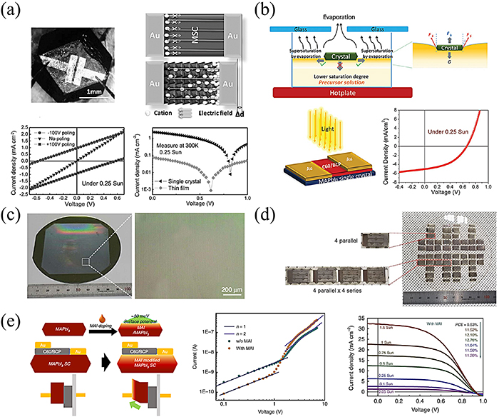
Figure 7. (a) Device structure, electric field distribution, switchable photovoltaic effect and photocurrents of a MAPbI3 lateral-structure single-crystal solar cell with poling [109]. John Wiley & Sons. [© 2016 John Wiley & Sons, Ltd.]. (b) Growth mechanism, device structure and PCE performance (@ 0.25 sun) of MAPbI3 single crystal through a bottom-up technique [49]. John Wiley & Sons. [© 2019 John Wiley & Sons, Ltd.]. (c) Photographic image of the perovskite thin films fabricated on a Si substrate by the GC-LCG process. Reproduced from [110]. CC BY 4.0. (d) Schematic illustration of the lateral single-crystal perovskite device with interdigitating in series and parallel [111]. John Wiley & Sons. [© 2020 John Wiley & Sons, Ltd.]. (e) Device structures, energy levels and trap measurement for lateral-structure devices w/o and with MAI treatment. The J-V curve of devices with MAI treatment under different light intensity (@ 0.05–1.5 Sun). Reproduced from [97]. CC BY 4.0.
Download figure:
Standard image High-resolution imageIn 2017, Sun et al developed a geometrically confined lateral crystal growth (GC-LCG) method that enabled fabricating thin MAPbI3 single crystals on a silicon substrate using a combination of hot-casting and lateral crystal growth, as shown in figure 7(c) [110]. This process enables the fabrication of single crystals with high carrier mobility and orientation. The PCE of the single-crystal, lateral-structured solar cells were 4.83%. By 2020, using the GC-LCG method, they have prepared a lateral-structured single-crystal cell with an efficiency of 9.50% under 0.1 sun illumination [111]. Based on this achievement, they fabricated interdigitated electrode units with high source-power generation in three distinct patterns: series (1 × 4), parallel (4 × 1), and combination (4 series × 4 parallel). These devices had respective PCEs of 7.99%, 8.19%, and 7.96% (figure 7(d)).
Large energy-level mismatches and surface defects between the anode and perovskite impeded the efficiency enhancement of lateral-structured, single-crystal cells. As shown in figure 7(e), Dong et al optimized the anode contact of single-crystal devices using a simple MAI surface treatment, resulting in fewer interface defects [97]. Meanwhile, the MAI treatment shifted the surface potential of the perovskite single crystal by ∼80 meV toward the valence band, which is advantageous for charge transfer in devices. Optimizing the anode contact considerably increased Voc (0.93 V) and FF (55.1%). Under 1 sun illumination, a record PCE for lateral-structured PSCs was obtained by achieving a PCE greater than 11%. Table 4 summarizes the performance of lateral-structured single-crystal solar cells [47, 97, 109–111]. The PSCs based lateral structured existed lower performance compared with vertically devices due to single crystal surface defects and functional interlayer energy level mismatch. These issues may be mitigated by interface passivation. Organic ammonium salts are a good choice for post treatment of perovskite surfaces. The performance of single-crystal PSCs is significantly improved after MAI treatment [52, 97]. In the future, other types of organic ammonium salts, such as phenylethylammonium iodide (PEAI) or butylammonium iodide (BAI), can be explored to optimize single-crystal PSCs stability and performance. However, it is still highly challenging to efficiently fabricate lateral-structured solar cells into photovoltaic module.
Table 4. Summary of parameters of lateral-structured, single-crystal solar cells.
| Materials | Device structure | Jsc (mA cm−2) | Voc (V) | FF (%) | PCE (%) | References |
|---|---|---|---|---|---|---|
| MAPbI3 Bulk | Au/perovskite/Au | 2.28 | 0.82 | — | 1.88 (0.4 sun) | [109] |
| MAPbI3 Wafer | Au/perovskite/PCBM/Ag | 18.33 | 0.801 | 32.9 | 4.83(1 sun) | [110] |
| MAPbI3 Wafer | Au/perovskite/C60/BCP/Au | 5.06 | 0.66 | 44 | 5.90 (0.4 sun) | [47] |
| MAPbI3 | Au/perovskite/TiO2/Ag | 3.35 | 0.75 | 0.46 | 9.50 (0.1 sun) | [111] |
| MAPbI3 thin crystal | Au/perovskite/C60/BCP/Au | 22.49 | 0.93 | 55.1 | 11.52(1 sun) | [97] |
5. Photodetectors based on perovskite single crystals
Single-crystal solar cells require maximum light energy conversion, which places increasingly stringent demands on device structure and single crystal quality. Photodetectors only need to recognize the optical signal and convert it to an electrical signal. Different application purposes have different requirements for the morphology, thickness and defect state of single-crystal materials. In addition, single-crystal materials have no grain boundary interference and high material uniformity, which are very important for fabricating micro-nano scale optoelectronic devices and ensuring the consistency of optoelectronic arrays. Hence, perovskite single crystals have greater potential for fabricating photo-signal detectors, and various studies have been conducted in this area. As for bulk single crystals, the simplest method for preparing devices is to evaporate the electrodes directly onto the crystal facet to build a metal-semiconductor-metal structure. However, the huge energy barrier of a metal-semiconductor heterojunction will severely limit the performance of the photodetector. Constructing a heterojunction is an effective method to solve this problem. In 2017, Huang et al used a thin single crystal as an active layer to fabricate a vertical p-i-n structure photodetector [112]. The crystal growth and device fabrication were comparable to the vertical single-crystal PSCs. It should be noted that the solar cell devices introduced in the previous section can also serve as visible-near IR broadband detectors, with similar principles and optimization methods to those in this chapter, and therefore are not repeated here. In this review, perovskite single crystal-based detectors are classified, based on their response to different wavelength ranges, as x-ray detectors, solar-blind UV photodetectors, visible (Vis) photodetectors, and IR photodetectors.
5.1. X-ray detectors
High-energy radiation is a form of electromagnetic wave with a wavelength of less than 10 nm and an energy range of more than 0.1 keV. It has a profound penetrating effect. High-energy radiation is used in many fields, including medical diagnosis, cancer treatment, material characterization, military reconnaissance etc [113–115]. Hence, developing high-performance radiation detectors is crucial.
There are two types of x-ray detectors: indirect and direct detectors. The classification is based on how the detector converts x-ray photons to electrical signals [116]. Indirect x-ray detection typically uses scintillators to transform x-rays into low-energy (UV or even Vis) photons, which are then converted into an electrical signal by optical detectors [117, 118]. Direct detectors convert x-ray photons directly into electrical currents, while an external circuit analyzes the accumulated charge [119]. Direct x-ray detectors feature a more straightforward manner of conversion, allowing them to provide a broad linear response range, a rapid pulse rise time, a high-energy resolution, and a high spatial resolution.
Because halide perovskites are made of ions with large atomic numbers (Pb2+, I−, and Br−), they have a high x-ray absorption capacity. X-rays with deep penetration require a much thicker active layer to absorb high-energy photons; hence, large single crystals of millimeter thicknesses are more suitable for x-ray detection than polycrystalline films. There are many kinds of structure for perovskite materials. Different components are suitable for different application scenarios of radiation detectors. So far, it can be roughly divided into 3D perovskite-based x-ray detectors, 2D perovskite-based x-ray detectors, and non-lead perovskite-based x-ray detectors.
5.1.1. 3D perovskite-based detectors.
In 2016, Huang et al reported the first sensitive x-ray detector constructed from a 2 mm thick MAPbBr3 single crystal [28]. As shown in figure 8(a), the x-ray detector-based structure of Au/MAPbBr3/C60/BCP/Au attained a charge collection efficiency of 16.4% for 50 keV x-rays at a near-zero bias condition, enabling the direct conversion of high-energy x-ray flux into collectible charges. Thus, the devices achieved a low detectable x-ray dose rate of 0.5 μGyair s−1 and a sensitivity of 80 μC  cm−2. Using solution-grown perovskite single crystals with a simple surface treatment can provide unexpectedly exceptional x-ray detection performance, indicating its potential utility in high-energy ray detection. Using brominated (3-aminopropyl) triethoxysilane molecules as a bonding agent, they developed a mechanically and electrically robust connection between MAPbBr3 single crystals and silicon substrates in 2017 (figure 8(b)) [120]. The dipole of the bonding molecule decreased the dark current of the device while retaining signal intensity. The Si-integrated detectors showed a very low detectable x-ray dose rate of <0.1 μGyair s−1 and a high sensitivity of 2.1 × 10⁴
μC
cm−2. Using solution-grown perovskite single crystals with a simple surface treatment can provide unexpectedly exceptional x-ray detection performance, indicating its potential utility in high-energy ray detection. Using brominated (3-aminopropyl) triethoxysilane molecules as a bonding agent, they developed a mechanically and electrically robust connection between MAPbBr3 single crystals and silicon substrates in 2017 (figure 8(b)) [120]. The dipole of the bonding molecule decreased the dark current of the device while retaining signal intensity. The Si-integrated detectors showed a very low detectable x-ray dose rate of <0.1 μGyair s−1 and a high sensitivity of 2.1 × 10⁴
μC  cm−2 when exposed to 8 keV x-rays, which were superior to the state-of-the-art commercial α-Se x-ray detectors. In 2020, Fang et al grew high-quality MAPbBr3 single crystals at room temperature by separating the solvent from the perovskite precursors using silicone oil [29]. Figure 8(c) shows the schematic of liquid-diffused, separation-induced crystallization (LDSC) of MAPbBr3 single crystals (LDSC-MAPbBr3). LDSC-MAPbBr3 exhibited a carrier lifetime of approximately 1 μs and a low trap density of 4.4 × 109 cm−3 compared to ITC-fabricated MAPbBr3. The 2 mm thick LDSC-MAPbBr3 single-crystal detectors demonstrated a sensitivity of 184.6 μC
  cm−2 and a measurable x-ray dose rate of 1.2 μGyair s−1 at −4 V. In 2021, x-ray detectors fabricated from FAPbBr3 single crystals could maintain high performance and stability at high operating temperatures [121]. FAPbBr3 single crystals maintained an excellent mobility lifetime product (1.1 × 10⁻² cm2) and a low electron trap density of (5.0 ± 0.2) × 109 cm−3. The detectors based on the Ga/FAPbBr3/Au structure can detect a minimum detectable dose rate of 0.3 μGyair s−1 with a sensitivity of 130 μC
  cm−2 under 0.5 V mm−1 electric field for 23.8 keV x-rays.

Figure 8. (a) Radiation detector structure, attenuation efficiency and x-ray-generated photocurrent of MAPbBr3 single crystals. Reproduced from [28], with permission from Springer Nature. (b) Schematic illustration of the fabrication of Si-integrated MAPbBr3 single crystals and its photograph. Reproduced from [120], with permission from Springer Nature. (c) Growth process of MAPbBr3 single crystals by LDSC method, corresponding TRPL spectral and x-ray detection performance. Reproduced from [29]. CC BY 4.0.
Download figure:
Standard image High-resolution imageAdditionally, compared to MAPbBr3 single crystals, MAPbI3 has promising applications in x-ray detection because of its higher μτ product and atomic number Z. Typically, nonrectangular dodecahedrons of the MAPbI3 single crystal limited the fabrication of flat-panel devices. Choy et al found the preferred growth of the (100) facet over the (110) facet in a halogen-rich precursor, which facilitated the synthesis of cuboid MAPbI3 single crystals (figure 9(a)) [122]. The cube shape imparts favorable geometry for device fabrication. Based on the (100) plane of MAPbI3, cuboid MAPbI3-based x-ray detectors exhibited a high sensitivity of 968.9 μC  cm−2 under a −1 bias. The crystal quality of active materials is the key to improving the performance of semiconductor electron devices. Density functional theory simulations suggested that mixing bigger ions with smaller MA+ at the A-site could reduce the interstitial defects and electron-phonon coupling strength of MAPbI3. As illustrated in figure 9(b), partial MA+ substitution with DMA+ (DMA = dimethylammonium) and GA+ (GA = guanidinium) produced DMAMAPbI3 and GAMAPbI3 single crystals [123]. Electrical characterizations confirmed that the alloyed GAMAPbI3 single crystal displayed improved charge collection efficiency and suppressed shallower defect density compared to the pristine MAPbI3 single crystal. Finally, the GAMAPbI3-based x-ray detectors demonstrated a sensitivity of 2.3 × 10⁴
μC
cm−2 under a −1 bias. The crystal quality of active materials is the key to improving the performance of semiconductor electron devices. Density functional theory simulations suggested that mixing bigger ions with smaller MA+ at the A-site could reduce the interstitial defects and electron-phonon coupling strength of MAPbI3. As illustrated in figure 9(b), partial MA+ substitution with DMA+ (DMA = dimethylammonium) and GA+ (GA = guanidinium) produced DMAMAPbI3 and GAMAPbI3 single crystals [123]. Electrical characterizations confirmed that the alloyed GAMAPbI3 single crystal displayed improved charge collection efficiency and suppressed shallower defect density compared to the pristine MAPbI3 single crystal. Finally, the GAMAPbI3-based x-ray detectors demonstrated a sensitivity of 2.3 × 10⁴
μC  cm−2 and a detectable x-ray dose rate of 16.9 μGyair s−1, which was superior to the pristine MAPbI3-based devices (2.5 × 10³
μC
cm−2 and a detectable x-ray dose rate of 16.9 μGyair s−1, which was superior to the pristine MAPbI3-based devices (2.5 × 10³
μC  cm−2). Later, numerous methods of fabricating high-quality crystals were presented. In the growing process of crystals, the growth rate of crystals reduces with time as the solute concentration drops below the level of supersaturation. This disrupts crystal growth and results in single crystals with imperfect structural perfection. Xu et al employed a continuous-mass transport process (CMTP) approach to solve this problem. The schematic illustration of the CMTP approach is shown in figure 9(c) [124]. This approach can uninterruptedly provide raw materials in the precursor solution for maintaining the MAPbI3 single crystal's steady growth at a constant growth rate. The CMTP-fabricated MAPbI3 exhibits a lower defect density (4.5 × 109 cm−3) and a higher mobility-lifetime product (1.6 × 10⁻³ cm2 V−1), allowing it to achieve ultrahigh x-ray detection performance comparable to that of a high-quality CdZnTe device. In 2021, Huang et al found that 3‐(decyldimethylammonio)‐propane‐sulfonate inner salt (DPSI) as an additive in the precursor solution can help to maintain the same crystal growth rate during the late period of growth, as shown in figure 9(d) [125]. Meanwhile, DPST additives interacting with Pb2+ and undercoordinated Pb can limit the probability of bonding or stacking incorrect ions, greatly enhancing the crystal quality. Finally, the devices showed a sensitivity of 2.6 × 10⁶
μC
cm−2). Later, numerous methods of fabricating high-quality crystals were presented. In the growing process of crystals, the growth rate of crystals reduces with time as the solute concentration drops below the level of supersaturation. This disrupts crystal growth and results in single crystals with imperfect structural perfection. Xu et al employed a continuous-mass transport process (CMTP) approach to solve this problem. The schematic illustration of the CMTP approach is shown in figure 9(c) [124]. This approach can uninterruptedly provide raw materials in the precursor solution for maintaining the MAPbI3 single crystal's steady growth at a constant growth rate. The CMTP-fabricated MAPbI3 exhibits a lower defect density (4.5 × 109 cm−3) and a higher mobility-lifetime product (1.6 × 10⁻³ cm2 V−1), allowing it to achieve ultrahigh x-ray detection performance comparable to that of a high-quality CdZnTe device. In 2021, Huang et al found that 3‐(decyldimethylammonio)‐propane‐sulfonate inner salt (DPSI) as an additive in the precursor solution can help to maintain the same crystal growth rate during the late period of growth, as shown in figure 9(d) [125]. Meanwhile, DPST additives interacting with Pb2+ and undercoordinated Pb can limit the probability of bonding or stacking incorrect ions, greatly enhancing the crystal quality. Finally, the devices showed a sensitivity of 2.6 × 10⁶
μC  cm−2 and a detectable x-ray dose rate of 5.0 μGyair s−1 for 60 kVp x-rays. However, 3D perovskite materials have lower EB and faster charge transport, which is not conducive to the accumulation and amplification of x-ray signals. In this regard, 2D perovskite materials have better adaptability.
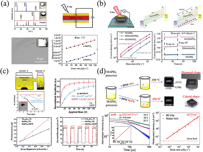
Figure 9. (a) The XRD pattern, SEM image, device structure, and detection performance of cuboid-MAPbI3 single crystals [122]. John Wiley & Sons. [© 2019 John Wiley & Sons, Ltd.]. (b) Architecture, x-ray photoresponse and generated photocurrent of the MAPbI3 based x-ray detectors [123]. John Wiley & Sons. [© 2019 John Wiley & Sons, Ltd.]. (c) Growth schematic and growth rate of MAPbI3 single crystal by CMPT, and hole mobility-lifetime products, photocurrent density, temporal response of corresponding device [124]. John Wiley & Sons. [© 2020 John Wiley & Sons, Ltd.]. (d) Scheme of crystals growing process, and photographs of the grown crystals w/o and with DPSI regulation. Time of flight transient currents and x-ray response current of Corresponding devices. Reproduced from [125]. CC BY 4.0.
Download figure:
Standard image High-resolution image5.1.2. 2D perovskite-based detectors.
Compared to 3D perovskites, 2D perovskites have a wider bandgap, better structural stability and larger EB. In 2020, 2D perovskite, BDAPbI4 (BDA=NH3C4H8NH3), single crystals were synthesized (figure 10(a)) [126]. The introduction of BDA2+ allows for the flexible control of the distance between adjacent inorganic layers to generate strong electrostatic interactions. Enhancing the structural stability and effective charge transport of BDAPbI4 single crystals is advantageous. The BDAPbI4-based x-ray detector showed a sensitivity of 242 μC  cm−2 with a measurable x-ray dose rate as low as 430 nGyair s−1. By aligning the benzene rings in the same orientation, Wei et al introduced fluorine atoms to PEA+ ions to enhance supramolecular interactions between organic spacers [127]. As shown in figure 10(b), strong interactions blocked the ion migration paths to stabilize and tune the electronic properties of (F-PEA)2PbI4 single crystals. The (F-PEA)2PbI4 single-crystal detector showed a remarkable sensitivity of 3402 μC
  cm−2 to 120 keV. Meanwhile, the lowest detected x-ray dosage rate was 23 nGyair s−1. Zhao et al have recently demonstrated for the first time how the halide-modulated molecular assembly affects the structure and characteristics of 2D perovskite single crystals [128]. Using an amidino-based organic spacer (3AP, 3-amidinopyridine), 2D (3AP)PbX4 (X=Cl, Br, and I) single crystals were effectively synthesized. Figure 10(c) depicts the images and crystalline structures of 2D (3AP)PbX4 (X=Cl, Br, and I) single crystals. Parallel and antisymmetric 3AP cations are placed between two inorganic layers. The halide transformation from I to Br and Cl resulted in greater Pb − X − Pb angles and a stronger hydrogen interaction, inhibiting ion migration in single crystals. The (3AP)PbCl4 exhibited an x-ray photoresponse with sensitivity up to 791.8 μC
  cm−2 and a low detection limit of 1.54 μGyair s−1.Owing to the toxicity of Pb, perovskite-based products containing Pb have been controversial. However, x-ray detection still have absorption coefficient requirements. It is necessary to study non-lead perovskite materials that meet the radiation detection requirements.
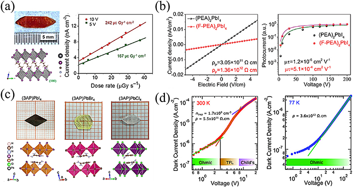
Figure 10. (a) The photograph, stacking structured, and x-ray response current of x-ray detectors based (BDA)PbI4 crystals [126]. John Wiley & Sons. [© 2020 John Wiley & Sons, Ltd.]. (b) The resistivity and photoconductivity of (PEA)2PbI4 and (F-PEA)2PbI4 single crystal [127]. John Wiley & Sons. [© 2020 John Wiley & Sons, Ltd.]. (c) Photographs and crystal structures of (3AP)PbX4 (X=I, Br, and Cl). Reprinted with permission from [128]. Copyright (2022) American Chemical Society. (d) SCLC characterization of Cs2AgBiBr6 single-crystal device at 300 and 77 K [130]. John Wiley & Sons. [© 2018 John Wiley & Sons, Ltd].
Download figure:
Standard image High-resolution image5.1.3. Non-lead perovskite-based detectors and others.
Bi is considered the most promising element to replace Pb in halide perovskite because its atomic radius is similar to Pb. Tang et al reported for the first time in 2017 the use of Cs2AgBiBr6 single crystals in fabricating x-ray detectors [129]. Under a 5 V bias, the detector exhibited a high sensitivity of 105 μC  cm−2 and a low detection limit of 59.7 nGyair s−1. The Ag+/Bi3+ disordering considerably affected the poor structural stability of the Cs2AgBiBr6 double perovskite, resulting in poor photoelectric properties. Roeffaers et al studied the temperature dependence of the photophysical properties of Cs2AgBiBr6 at room and liquid nitrogen (LN2T) temperatures [130]. By cooling Cs2AgBiBr6 to LN2T, lattice defects induced by structural distortion were considerably reduced, resulting in enhanced free-carrier transporting efficiency (figure 10(d)). Therefore, the x-ray detectors exhibited better performance with a sensitivity of 988 μC
  cm−2 near LN2T than at room temperature, which was 316 μC
  cm−2. Fan et al found that phenylethylamine bromide (PEABr) enables the in situ regulation of the alternatively ordered arrangement of Ag+ and Bi3+ ions in the Cs2AgBiBr6 single crystal [131]. The experimentally established and the enhanced ordering extent of the [BiX6]3− and [AgX6]5− octahedral can inhibit the formation of self-trapped excitons, contributing to the carrier drift distance. As shown in figure 11(a), the corresponding detectors based on PEA-Cs2AgBiBr6 exhibit a very high sensitivity of 288.8 μC
  cm−2, which was two times greater than that of the reference Cs2AgBiBr6 (165.6 μC
  cm−2).
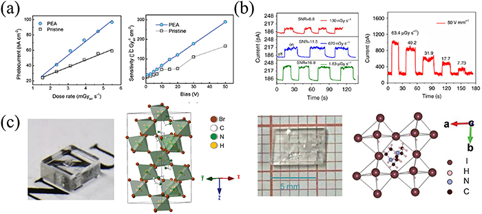
Figure 11. (a) Photocurrent intensity and sensitivity of x-ray detectors based Cs2AgBiBr6 and PEA-Cs2AgBiBr6 single crystal [131]. John Wiley & Sons. [© 2019 John Wiley & Sons, Ltd.]. (b) x-ray photocurrent response and thermal stability test of Cs3Bi2I9 single-crystal detectors. Reproduced from [133]. CC BY 4.0. (c) The optical image and crystal structure of DABCO-NH4Br3 and MDABCO-NH4I3, respectively [75]. John Wiley & Sons. [© 2020 John Wiley & Sons, Ltd]. [76], John Wiley & Sons. [© 2021 John Wiley & Sons, Ltd].
Download figure:
Standard image High-resolution imageIn addition to Cs2AgBiBr6 single crystals, some double perovskites are fabricated for higher x-ray performance. Yang et al fabricated an (NH4)3Bi2I9 single-crystal x-ray detector [132]. The devices demonstrated high sensitivity (8.2 × 10³
μC  cm−2) and a low detection limit (55 nGyair s−1). In 2020, Liu et al synthesized large-sized Cs3Bi2I9 single crystals via a nucleation-controlled solution method [133]. The nucleation-controlled method is realized by refining the precursor solution. The detector based on the Cs3Bi2I9 single crystal showed a sensitivity of 1146.7 μC
  cm−2. Meanwhile, Cs3Bi2I9 single crystals showed an excellent thermodynamic, stability-assured x-ray detector with a stable response at a temperature of 100 °C for a long time under continuous x-ray illumination and a high electric field (63.4 μGyair s−1, 50 V mm−1), as shown in figure 11(b).
Recently, Zhao et al synthesized metal-free halide perovskite single crystals, such as DABCO-NH4Br3 (DABCO=N-N'-diazabicyclo[2.2.2] octonium) [75], and MDABCO-NH4I3 (MDBACO=methyl-N'-diazabicyclo[2.2.2] octonium) [76], as shown in figure 11(c). The environmentally friendly, metal-free halide perovskites can be fabricated from an aqueous solution and are fully degradable when rinsed with water. DABCO-NH4Br3, for instance, showed very high charge diffusion lengths (tens of μm), contributing to a sensitivity of up to 173 μC  cm−2 for a 29 keV x-ray.
As shown in table 5, perovskite single-crystal x-ray detectors achieved impressive performance, and that stability and environmental friendliness have gradually been resolved through the continuous development of material systems, issues [28, 29, 75, 76, 120–123, 125–139]. However, the solution method has the drawbacks of limited size and high time cost, which hinder the preparation of large area detectors and their commercial applications. A vapor-phase epitaxy deposition is a potential solution. For example, Liu et al Grown large-scale thin CsPbBr3 single crystal film on sapphire substrate via chemical vapor deposition.
Table 5. Key parameters of perovskite single crystal-based x-ray detectors.
| Materials | Sensitivity (μC  cm−2) cm−2) | Lowest detectable x-ray dose rate (μGyair s−1) | Devise structure | References |
|---|---|---|---|---|
| MAPbBr3 | 80 | 0.5 | Au/perovskite/C60/BCP/Ag or Au | [28] |
| Si-integrated MAPbBr3 | 2.1 × 10⁴ | <0.1 | Si/perovskite/C60/BCP/Au | [120] |
| MAPbBr3 | 184.6 | <1.2 | InGa/C70/perovskite/Au | [29] |
| FAPbBr3 | 130 | 0.3 | Ga/perovskite/Au | [121] |
| MAPbI3 | 968.9 | — | Au/Cr/perovskite/Cr/Au | [122] |
| GA- MAPbI3 | 2.3 × 10⁴ | 1.7 × 10⁻² | Ga/perovskite/Au | [123] |
| MAPbI3 | 5.2 × 10⁶ | 0.1 × 10⁻³ | Au/BCP/C60/perovskite/MoO3/Au | [134] |
| MAPbI3 | (2.6 ± 0.4) × 106 | (5.0 ± 0.7) × 10−3 | Cr/Oxysalt/perovskite/Oxysalt/C60/BCP/Cr | [125] |
| MAPbX3 cascade single crystal | 1.6 | — | Gd or Ag/perovskite/Au | [135] |
| BDAPbI4 | 242 | 0.43 | Au/perovskite/Au | [126] |
| (F-PEA)2PbI4 | 3402 | 2.3 × 10⁻² | Au/perovskite/C60/BCP/Cr | [127] |
| (3AP)PbX4 | 791.8 | 1.54 | Au/perovskite/Au | [128] |
| DABCO-NH4Br3 | 173 | 4.960 | Au/perovskite/Au | [75] |
| MDABCO-NH4I3 | 1997 ± 80 | — | Au/perovskite/Au | [76] |
| [(CH3)3NH]MnCl3 | 295 | 0.90 | Au/perovskite/Au | [136] |
| Cs2AgBiBr6 | 105 | 6.0 × 10⁻² | Au/perovskite/Au | [129] |
| Cs2AgBiBr6 | 988 | — | Au/perovskite/Au | [130] |
| PEA- Cs2AgBiBr6 | 288.8 | — | Ga/perovskite/Ga | [131] |
| Cs2AgBiBr6 wafers | 250 | 95.3 × 10⁻³ | Au/perovskite/Au | [137] |
| (NH4)3Bi2I9 | 8.2 × 10³ | 55 × 10−3 | Au/perovskite/Au | [132] |
| Cs3Bi2I9 | 1652.3 | 0.130 | Au/perovskite/Au | [133] |
| Rb3Bi2I9 | 159.7 | 8.32 | Au/perovskite/Au | [138] |
| (4,4-difluoropiperidinium)4 AgBiI8 | 188 | 3.13 | Au/perovskite/Au | [139] |
5.2. Solar-blind UV detectors
UV light refers to a specific electromagnetic radiation band with a 10–400 nm wavelength range and an energy distribution range of 3.1–12.4 eV [140]. UV light detection technology has been critical in the biomedical imaging, fire monitoring, and military fields [141]. Traditional narrow band gap (1.5–1.6 eV) perovskite materials have difficulty in recognizing UV light due to the interference of the full-spectrum. Therefore, there is a need for developing solar-blind UV detectors. Wide bandgap halide perovskites have shown great potential in recent years.
5.2.1. 3D perovskite-based detectors.
The bandgap of the MAPbCl3 perovskite is approximately 2.9 eV, making it an appropriate active layer material for UV light detectors. In 2015, Bakr et al developed a centimeter-sized MAPbCl3 single crystal using the ITC method and fabricated a UV light photodetector for the first time (figure 12(a)) [60]. The device exhibited UV light sensitivity with a spectrum responsivity of 46.9 mA W−1, detectivity of 1.2 × 10¹⁰ Jones, and fast response speed of 24 ms under an applied bias of 15 V and 365 nm UV illumination (1 W cm−2). Although the rapid growth rate of the ITC method enables the formation of enormous single crystals in a matter of hours, high-temperature growth results in a substantial number of single-crystal defects. A novel, two-step, thermal procedure, high-quality MAPbCl3 has been developed. This method involves two growth processes: lower-temperature nucleation and higher-temperature crystallization [142]. The fabricated MAPbCl3 single crystal has a lower defect density (∼7.9 × 109 cm−3) than the ITC-grown MAPbCl3 crystals. As a result, the responsivity and detectivity of the detector employing the optimized MAPbCl3 crystal were increased to 3730 mA W−1 and 9.97 × 10¹¹ Jones at 415 nm, respectively. In addition, the devices exhibited a quick response time of 130 ns. Bakr et al reported the fabrication of a photodetector with the structure ITO/MAPbCl3/spiro-OMeTAD/Au using an μm-thick MAPbCl3 single crystal [143]. Their photodetectors showed an excellent self-powered character without consuming external power, ascribed to a p-n junction at the interfaces of perovskite/Spiro-OMeTAD. As shown in figure 12(c), the detectors exhibit a high specific detectivity of 6 × 10¹² Jones, a responsivity of 134 mA W−1, and 42.9% EQE when illuminated by 400 nm light.

Figure 12. (a) Device architecture and energy band diagram of the UV-photodetector based MAPbCl3 single-crystals. Reprinted with permission from [60]. Copyright (2015) American Chemical Society. (c) PL spectrum of the (PEA)2PbBr4 single crystals. Inset: The photograph of a single crystal with and without a UV lamp. The responsivity and detectivity dependence for (PEA)2PbBr4 photodetector with 365 nm light irradiance. [143]. John Wiley & Sons. [© 2019 John Wiley & Sons, Ltd.]. (b) The EQE, responsivity and current density-voltage curves of UV photodetectors based thin single crystals Reproduced from [62] with permission from the Royal Society of Chemistry. (d) Schematic working mechanism of the ferro-pyro-phototronic effect of the PMA2PbCl4 photodetectors as turning on and turning off the laser. Reprinted with permission from [65]. Copyright (2022) American Chemical Society.
Download figure:
Standard image High-resolution image5.2.2. 2D perovskite-based detectors.
Single crystals of 2D perovskite (PEA)2PbBr4 have a bandgap width of Eg = 2.91 eV, making them also ideal for use in UV photodetectors. Liu et al synthesized a large-size (PEA)2PbBr4 single crystal using the controlled evaporation method [62]. With a bias of 10 V, the fabricated detector-based (PEA)2PbBr4 exhibited responsivity, detectivity, and rapid response rates of 31.48 mA W−1, 1.55 × 10¹³ Jones, and 0.4 ms, respectively, when illuminated by a 365 nm LED (figure 12(b)). Subsequently, Zhou et al developed a gas-liquid interface crystalline route to grow a BA2PbBr4 (BA=CH3CH2CH2CH2NH3 +) single crystal [64]. The nucleation energy barrier difference between the solution surface and volume gave the precursor molecules a higher chemical potential in the initial state at the gas-liquid interface, resulting in a crystal nucleus at this interface. Moreover, a thin crystal will preferentially grow along the side parallel to the surface of the solution under the buoyancy and surface tension effect. Under 400 nm illumination and a 4 V bias, BA2PbBr4 thin crystals exhibited a heightened UV light response with an efficient responsivity of 45 mA W−1 and a detectivity of ∼1012 Jones.
Notably, the ferroelectric photovoltaic effect has been observed in 2D perovskite materials. This effect can separate electron-hole pairs via the spontaneous, polarization-induced, built-in electric field, making self-powered photodetection possible [65, 144]. Based on this, Yang et al fabricated a self-powered UV photodetector using a PMA2PbCl4 monocrystalline sheet [65]. When illuminated by UV light, a built-in ferroelectric field of PMA2PbCl4 can generate and separate photoinduced carriers, forming a stable photocurrent (figure 12(d)). Meanwhile, spontaneous polarization and bound charges decreased with the increasing irradiation temperature, generating a positive output pyroelectric current. At zero bias, the devices exhibited a responsivity of 9000 mA W−1 and a detectivity of 1.01 × 10¹¹ Jones for 320 nm UV light.
As shown in table 6, the detection performance of single-crystal solar-blind UV detectors has gradually improved, but the detection wavelength range is only focused in the near ultraviolet region [60–65, 142–147]. Detecting the deep ultraviolet region remains a challenge for future research. One possible solution is to broaden the band gap of perovskite single crystals through designedly doping or component engineering. Luo et al reported a wide band gap 2D perovskite ferroelectric, (isobutylammonium)2(methylamium)Pb2Cl7, achieved photoresponse under 266 nm illumination [148].
Table 6. The important parameters of UV light detectors reported in the literature.
| Materials | Wavelength (nm) | Responsivity (mA W−1) | Detectivity (Jones) | τrise/τfall (μs) | Dark current (A) | References |
|---|---|---|---|---|---|---|
| MAPbCl3 | 365 nm | 46.9 | 1.2 × 10¹⁰ | 2.4 × 10⁴/6.2 × 104 | 4 × 10⁻⁷/5 V | [60] |
| Cs2AgInCl6 | 360 nm | 32 | ∼1012 | 970 | 1 × 10⁻¹¹/5 V | [61] |
| MAPbCl3 | 415 nm | 3730 | 1.0 × 10¹² | 0.13 | 5.23 × 10⁻⁸/15 V | [142] |
| MAPbCl3 thin single crystals | 400 nm | 134 | 6 × 10¹² | 0.015 | 1.4 × 10⁻⁸/− 0.1 V | [143] |
| (PEA)2PbBr4 | 365 nm | 31.48 | 1.6 × 10¹³ | 400/370 | ∼1013/10 V | [62] |
| CsPbCl3 microplatelets | 405 nm | 450 | 1011 | 8 × 10³/7 × 104 | 2.2 × 10⁻¹²/5 V | [63] |
| (BPA)2PbBr4 | 377 nm | 10 | 107 | 27/30 | 1.2 × 10⁻¹⁴/0 V | [144] |
| PMA2PbCl4 | 320 nm | 9000 | 1.0 × 10¹¹ | 162/226 | — | [65] |
| BA2PbBr4 | 400 nm | 45 | ∼1012 | 9.7 × 10³/8.8 × 103 | ∼10−14 | [64] |
| MAPbCl3 sheet | 395 nm | 880 | 2.3 × 10¹¹ | — | 8 × 10⁻⁹/3 V | [145] |
| [(R)-MPA]2PbCl4 onto Si wafers | 266 nm | 2 | 1.2 × 10¹² | 150/150 | 6 × 10⁻¹⁴/0 V | [146] |
| MAPbCl3 | 430 nm | 4 | 1.05 × 10¹⁰ | 1.3 × 10⁵/1.9 × 104 | — | [147] |
5.3. Photodetectors for visible wavelength
Visible light detectors are essential for the modern electronics industry and have wide applications in image information capture, industrial automation and machine vision illumination. To facilitate the discussion, the visible light detectors be classified based on the perovskite crystal structure.
5.3.1. 3D perovskite-based detectors.
In 2015, Huang et al reported the first photodetector based on a halide perovskite single crystal [1]. The spectral response of the resulting MAPbBr3 − x Clx and MAPbI3 − x Brx mixed halide perovskite was continuously tunable from blue to red (figure 13(a)). With these single crystals, the photodetector exhibited constantly tunable ultra-narrow photodetection in the visible region, with a full-width, half-maximum of <20 nm for the EQE peak. Although the devices had low detectivity compared to commercial InGaAs photodetectors, they can be further improved by optimizing the quality of the single crystals. A planar-type photodetector based on the (100) facet of a MAPbI3 single-crystal bulk was fabricated in the same year [149]. Due to the excellent properties of the MAPbI3 single crystal, the performance of the detectors was considerably enhanced compared to their polycrystalline film counterparts. With a 1 V bias, even devices with a simple structure (Au/perovskite/Au) exhibited a high R-value of 953 A W−1 and an EQE of 222 000%. Meanwhile, the transient photocurrent measurement demonstrated the quick response speed (74 μs/58 μs) of the photodetector. Liu et al sliced a large-sized MAPbI3 single crystal to a millimeter-thick, single-crystalline wafer via the crystal-slicing method and integrated ∼100 photodetectors on a piece of wafer, as shown in figure 13(b) [69].
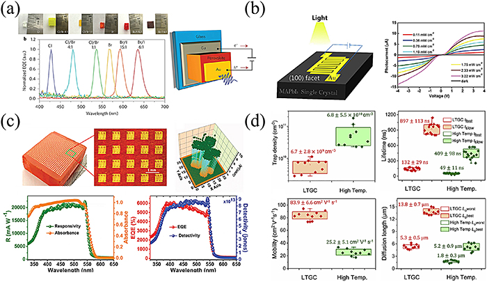
Figure 13. (a) The photograph, normalized PL spectra of MAPbBr3−x Clx and MAPbI3−x Brx single crystals, and its devices structure of photodetectors. Reproduced from [1], with permission from Springer Nature. (b) Planar-type structure and I-V curves of MAPbI3 photodetector irradiated by a 532 nm laser. Reproduced from [149]. CC BY 4.0. (c) The photograph, responsivity, EQE, detectivity and imaging of the photodetectors based on MAPbBr3 bulk single crystals with illuminated wavelength changing from 325 to 650 nm [66]. John Wiley & Sons. [© 2018 John Wiley & Sons, Ltd.]. (d) Trap density, carrier mobility, average carrier lifetime and diffusion length of MAPbBr3 single crystals obtained w/o and with LTGC treatment. Reprinted from [41], Copyright (2019), with permission from Elsevier.
Download figure:
Standard image High-resolution imageOptimizing the crystal growth is critical to improving the detector's performance. By investigating the crystal nucleation and growth dynamics, Liu et al summarized an LTGC strategy to generate high crystalline MAPbBr3 [66]. As shown in figure 13(c), the MAPbBr3 single crystal synthesized using the low-temperature strategy showed a long carrier lifetime (∼900 ns), high carrier mobility (81 ± 5 cm2 V−1 s−1), and low trap density (6.2 ± 2.7 × 109 cm−3), and its photodetectors achieved a high responsivity and detectivity of 16 A W−1 and 6 × 10¹³ Jones, respectively, under 525 nm illumination at 4 V bias. Notably, they designed an imaging assembly comprised of 729 pixel array sensors that can accurately distinguish the projected optical patterns on the imaging components. A new study was conducted on the nucleation and growth dynamics of the LTGC strategy [41]. The single-crystal growth model can be divided into three primary regions: the unsaturated, oversaturated, and optimized growth regions, separated by the solubility curve (S-T curve) and nucleation curve (N-T curve). At the optimized growth region, crystallization occurs solely on the existing nucleation seed, but there is not enough energy to exceed the nucleation energy to form a new crystal nucleus and limit extraneous nucleation. In addition to preventing the extraneous nucleation of single crystals, the formation of high-quality crystals also requires an appropriate development rate. As illustrated in figure 13(d), single crystals exhibit excellent electrical properties when the optimal growth temperature and heating rate are selected. These excellent optoelectronic properties were further translated into the highest sensor performance, including a high responsivity of 55.7 A W−1, EQE of 13 453%, detectivity of 8 × 10¹³ Jones, and response time of 15.8 μs.
5.3.2. 2D perovskite-based detectors.
2D perovskite materials with narrow bandgap can also be used as active material for visible photodetectors. Large organic cations, such as PEA+ (PEA=C6H5C2H4NH3), can inhibit the formation of shallow impurities during crystallization. The x-ray diffraction patterns and optical images of PEA2PbI4·(MAPbI3)n − 1 (n = 1, 2, 3) single crystals are depicted in figure 14(a). (PEA)2PbI4·(MAPbI3)n − 1 (n = 1, 2, and 3) exhibited self-doping concentrations that were three orders of magnitude lower than those of 3D hybrid perovskites. The corresponding photodetectors showed a detectivity of 1.1 × 10¹³ and a responsivity of 0.15 A W−1 for an n value of 1. Using an induced peripheral crystallization approach, large, area-flexible (PEA)2PbI4 single crystals have been created to meet the needs of flexible wearable electronic device design [150]. Figure 14(b) demonstrates that plate-like (PEA)2PbI4 crystals achieved a large area exceeding 2500 mm2 and a controlled micron-thickness maximum bending angle greater than 190°. As an application in flexible photodetectors, the highest R, EQE, and D* are measured to be 98.17 A W−1, 26 500%, and 1.62 × 10¹⁵ Jones, respectively, at 460 nm wavelength and 4 V bias. Based on the anisotropy of the crystal, they also found that the carrier-carrying performance of the (100) facet of (PEA)2PbI4 is superior to the (010) facet [151]. Figure 14(c) illustrates that, according to a series of electrical performance measurements, the average carrier life, trap density, and μτ measurement along the (001) facet are superior to those along the (010) facet. Hence, the device on the (001) plane exhibits a very high R of 139.6 A W−1, an EQE of 37 719.6%, a D* of 1.89 × 10¹⁵ Jones, and a rapid response speed of 21 μs/37 μs.

Figure 14. (a) XRD patterns and corresponding optical images of PEA2PbI4·(MAPbI3)n −1 (n = 1, 2, 3) single crystals. Reprinted with permission from [159]. Copyright (2017) American Chemical Society. (b) Optical images showing the flexing angle measurement for the micron-thickness (PEA)2PbI4 single crystals. Reproduced from [150]. CC BY 4.0. (c) Schematic diagram of carrier transporting and crystal structures on the (001) and (010) planes of a 2D (PEA)2PbI4 single crystals. Reprinted from [151], Copyright (2019), with permission from Elsevier. (d) Responsivity and detectivity of 2D (C4H9NH3)n (CH3NH3)n − 1Pbn I3n + 1 photodetectors with different n values. Reprinted with permission from [152]. Copyright (2018) American Chemical Society.
Download figure:
Standard image High-resolution imageAdditionally, scientists have developed various 2D perovskite single crystals, such as (BA)n (MA)n − 1Pbn I3n + 1 (n = 1, 2, 3,4, and ∞) [152], BDAPbI4 [153], and demonstrated their application in a single-crystal photodetector. For (BA)n (MA)n − 1Pbn I3n + 1, reducing the thickness of the quantum well can effectively limit the charge transfer. As shown in figure 14(d), the excellent charge transporting behavior will allow the devices based on (BA)n (MA)n − 1Pbn I3n + 1 to exhibit the highest on/off ratio of ∼104 and the lowest dark current of ∼10−13A as an n value of 1. However, the thinner quantum wells enlarged the EB energy of 2D materials, limiting the detectivity and responsivity of photodetectors. At n = ∞, the detectors achieved the highest detectivity of 2.4 × 10¹³ Jones and a responsivity of 38 A W−1. Perovskite single crystals vis-light detectors have been realized excellent performance such as high responsivity and ultrafast response speed (see table 7) [1, 41, 66–69, 71, 72, 86, 112, 149–159]. In the future, the research direction of single crystal vis-light detectors will gradually shift from improving performance to functional development to achieve the building of multi-functional, high-performance, and multimode optical detector systems, such as polarized light detections [160] and spectrometers [161, 162].
Table 7. The important parameters of Visible light photodetectors reported in the literature.
| Materials | Wavelength (nm) | Responsivity (mA W−1) | Detectivity (Jones) | τrise/τfall (μs) | References |
|---|---|---|---|---|---|
| MAPbBr3−x Clx /MAPbI3 − x Brx | 570 nm | — | 2 × 10¹⁰/− 4 V | ∼ 4 | [1] |
| MAPbI3 | 532 nm | 9.53 × 10⁵/1 V | — | 74/58 | [149] |
| CsPbBr3 | 550 nm | 28 | 1.7 × 10¹¹/0 V | 2.3 × 10⁵/6 × 104 | [68] |
| MAPbBr3 | 540 nm | 260 | 1.5 × 10¹³ | 0.1 | [112] |
| MAPbI3 | 780 nm | 320 | 1.5 × 10¹³ | 0.35 | [112] |
| MAPbI3 | 400–750 nm | ∼5 × 10³ | — | 39/1.9 | [69] |
| MAPbBr3 | 525 nm | 1.6 × 10⁴/4 V | 6 × 10¹³ | 40 | [66] |
| MAPbBr3 thin single crystals | 405 nm | 1.6 × 10¹⁰ | 1.3 × 10¹³ | 81/892 | [86] |
| MAPbBr3 | 515 nm | 5.57 × 10⁴/5 V | 8 × 10¹³ | 27.6/15.8 | [41] |
| Si/MAPbBr3 | 520 nm | 13.6/− 1 V | 5.9 × 10¹⁰ | 0.52/2.44 | [154] |
| MAPbBr3 P-N junction | 520 nm | 620/0 V | 2.16 × 10¹² | — | [155] |
| MAPbBr3 N-P-N junction | 520 nm | 1.45 × 10⁴/8 V | 4.67 × 10¹³ | — | [155] |
| MAPbBr3 | 554 nm | 3.21 × 10⁵ | — | 15.1/2.1 | [156] |
| MAPbBr3 thin single crystal | 532 nm | 1.02 × 10⁶ | 2.02 × 10¹³ | 2.1 × 10⁵/2.6 × 105 | [67] |
| MAPbI3 (100) plane | 400 nm | 160/0 V | 7.34 × 10¹¹ | 1.5 × 10⁵/5 × 104 | [157] |
| CsPbBr3 | 520 nm | 2.78 × 10⁵/3 V | 4.36 × 10¹³ | — | [158] |
| Cs3Bi2I9 | White LED | 7.2 | 1.0 × 10¹¹ | 247/230 | [71] |
| Cs2AgBiBr6 | 550 nm | 4.88 × 10³ | 1.22 × 10¹³ | 8/8.8 | [72] |
| (C6H5C2H4NH3)2PbI4·(CH3NH3PbI3)n −1 | 500 nm | 150 | 1013 | — | [159] |
| (C4H9NH3)n (CH3NH3)n −1 Pbn I3n+1 (n = 1) | — | 3.8 × 10⁴ | 2.1 × 10¹³ | 1.7/3.9 | [152] |
| (PEA)2PbI4 | 460 nm | 9.82 × 10⁴/4 V | 1.62 × 10¹⁵ | 64/52 | [150] |
| (PEA)2PbI4 | 462 nm | 1.40 × 10⁵/5 V | 1.89 × 10¹⁵ | 21/37 | [151] |
| BDAPbI4 | 462 nm | 927/4 V | 1.23 × 10¹¹ | 187/163 | [153] |
5.4. Photodetectors for IR wavelength
IR photodetectors, which can detect light within the wavelength range of 0.8–30 μm, have gained considerable research interest during the past years [163, 164]. It is widely used in optical communication, light-lidar, thermal imaging and other fields. The development of component engineering of perovskites, especially that of narrow-bandgap perovskite materials, is particularly rapid and promotes the application of perovskite materials in IR detection [165, 166]. MAPbI3 single crystals exhibit a much stronger near-IR (NIR) photoresponse than polycrystalline film, well below the optical gap (shown in figure 15(a)). For example, Meredith et al measured MAPbI3-based photodiodes and found that the devices have a photoresponse to a 1064 nm wavelength laser below the bandgap [167]. In addition, other studies have reported that photodetector-based MAPbI3 single crystals had a responsivity of 568 A W−1 under the IR illumination of 895 nm [168]. Li et al constructed a microscopic imaging system relying on MAPbI3-based IR detectors and NIR bioimaging of the mouse organs [169]. As shown in figure 15(b), the NIR images of the different mouse organs corresponded to their real-world counterparts.
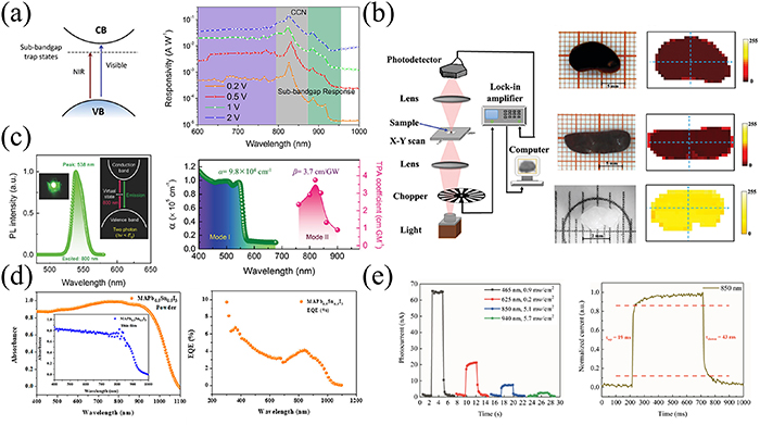
Figure 15. (a) Schematic diagram of sub-gap electron trap state absorptions, and corresponding photoresponse at below gap (NIR, 900 nm) light illumination for MAPbI3 photodetector [167]. John Wiley & Sons. [© 2017 John Wiley & Sons, Ltd.]. (b) Structure of the microscopic NIR imaging system based MAPbI3 single-crystal photodetector. The picture and corresponding NIR image of mice organs. Reproduced from [169] with permission from the Royal Society of Chemistry. (c) The visible optical absorption coefficient (α and β) and photoluminescence spectrum of CsPbBr3 single crystals. Reproduced from [171] with permission from the Royal Society of Chemistry. (d) The absorption spectra of MAPb0.5Sn0.5I3 single-crystal devices, and its EQE curves and photodetectors, respectively. Reproduced from [73]. CC BY 4.0. (e) Photocurrent switching and response times of photodetectors based on PbS doping MAPbI3 single crystals under 850 nm light illumination [170]. John Wiley & Sons. [© 2022 John Wiley & Sons, Ltd].
Download figure:
Standard image High-resolution imageTin (Sn) doping is an effective strategy for reducing the optical bandgap of MAPbI3 single crystals. For example, the MAPb0.5Sn0.5I3 single crystal expanded the absorption range to approximately 950 nm, as shown in figure 15(d) [73]. Under 905 nm NIR light irradiation, the as-fabricated detectors achieved a responsivity of 0.514 AW−1 and a specific detectivity of 1.4974 × 10¹¹ Jones. In addition to Sn doping, adding lead sulfide quantum dots to an MA-based single crystal enabled the extension of the photoresponse range [74, 170]. At 850 nm illumination and 10 V bias, the IR photodetectors' responsivity and detectivity reached 0.02 mA W−1 and 1.2 × 10⁸ Jones, respectively. Figure 15(e) demonstrates that the device achieved a response time of ∼19 ms.
Zeng et al found that CsPbBr3 exhibited not only a high visible absorbance coefficient but also a high nonlinear IR absorption coefficient, which is related to two-phonon absorption [171]. Hence, all inorganic CsPbBr3 can be used to construct Vis-IR dual-modal photodetectors and achieve a light on/off ratio of 500 under 800 nm laser excitation (figure 15(c)). Table 8 summaries the performance of IR photodetectors in past years [73, 74, 168–171]. There have been significant improvements in the performance, but for IR photodetectors, thermal stability remains a long- term challenge. Controlling the composition of A-site cations is an effective solution. Paetzold et al identified compositions of formamidinium and cesium to result in the most stable perovskite compositions with respect to thermal stress [172].
Table 8. The important parameters of IR photodetectors reported in the literature.
| Materials | Wavelength (nm) | Responsivity (mA W−1) | Detectivity (Jones) | τrise/τfall (μs) | References |
|---|---|---|---|---|---|
| CsPbBr3 | 800 nm | 2 × 10³ | — | 69/261 | [171] |
| MAPbI3 | 895 nm | ∼5.68 × 10⁵ | 5.5 × 10¹⁵ | 2.2 × 10⁵/1.6 × 105 | [168] |
| MAPb0.5Sn0.5I3 | 905 nm | 514/− 1 V | 1.50 × 10¹¹ | — | [73] |
| PbS QDs MAPbCl0.5Br2.5 | 850 nm | 0.02/10 V | 1.2 × 10⁸ | 1.9 × 10⁴/4.3 × 104 | [170] |
| MAPbI3 | 800 nm | 1080/5 V | 1.77 × 10¹² | ∼125/∼ 1.93 × 10³ | [169] |
| Cs3Bi2I9 | 4000 nm | 6.5 × 10⁻⁴ | 8.7 × 10⁸ | <4 × 10⁶/1 × 107 | [74] |
6. LEDs and lasers
Perovskite single crystals can not only use the characteristics of absorbing photons to convert into electrons to make high-efficiency solar cells and detectors, but also use photon emission properties to make high-brightness LEDs and lasers. However, LEDs and lasers have different working principles. An LED applies a current across the perovskite single crystal to excite photons through radiative recombination, while a laser employs an external pump source to induce the perovskite single crystal to undergo stimulated emission and generate a monochromatic, coherent beam [173, 174]. Yu et al manipulates the ion migration to create a p-i-n structure in MAPbBr3 crystals, and stabilized it by low-temperature treatment [175]. Based on this, they fabricated a LED that emit 2.3 eV photons (green light) starting at 1.8 V, and can operate continuously for 54 h at a brightness of ∼5000 cd m−2 without significant degradation. The p-i-n structure formed by ion migration suffers from severe instability, thus Pan et al employs CsPbBr3 nanocrystal arrays as the emissive layer to fabricate a multilayer device with a configuration of ITO/NiO/CsPbBr3/poly(methyl methacrylate) (PMMA)/ZnO/Ag, as shown in figure 16(a) [176]. The device exhibits highly stable electroluminescence (EL) within the wavelength range of 520–560 nm. They successfully fabricated a 62 × 47 nano-array device, and achieved a 99% working ratio. In 2022, Jie et al devises a facile liquid-insulator bridging (LIB) strategy to produce high-brightness LED devices based on MAPbBr3 micro-crystals [177]. They suppress the internal leakage current and electrode short circuit issues of the device by inserting PMMA insulating layer. The preparation process of the device is illustrated in the figure 16(b). The LIB strategy can also control the crystal growth and optimize the device architecture to enhance the performance of LED devices. The optimal LED device achieved an ultrahigh luminance of 136 100 cd m−2 and a half-lifetime of 88.2 mins at an initial luminance of 1100 cd m−2. Recently, Xiao et al employed a synergistic approach of perovskite component engineering and precursor additive engineering, which markedly enhanced the external photoluminescence quantum yield of perovskite single crystals to 28.3% [178]. Using perovskite crystals with a thickness of 1.5 μm as the active layer, they produced LED devices with an ultrahigh luminance of 86 000 cd m−2 and a peak EQE of 11.2%, and achieved a T50 lifetime of 12 500 h at an initial luminance of 100 cd m−2. (figure 16(c)).
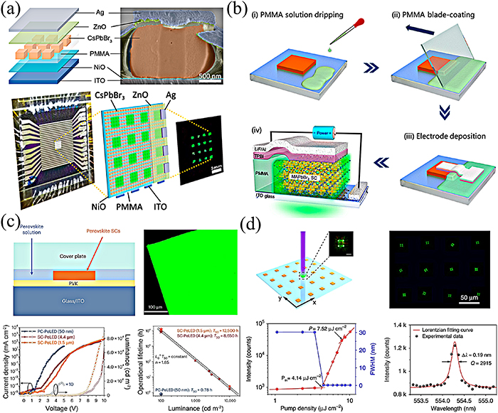
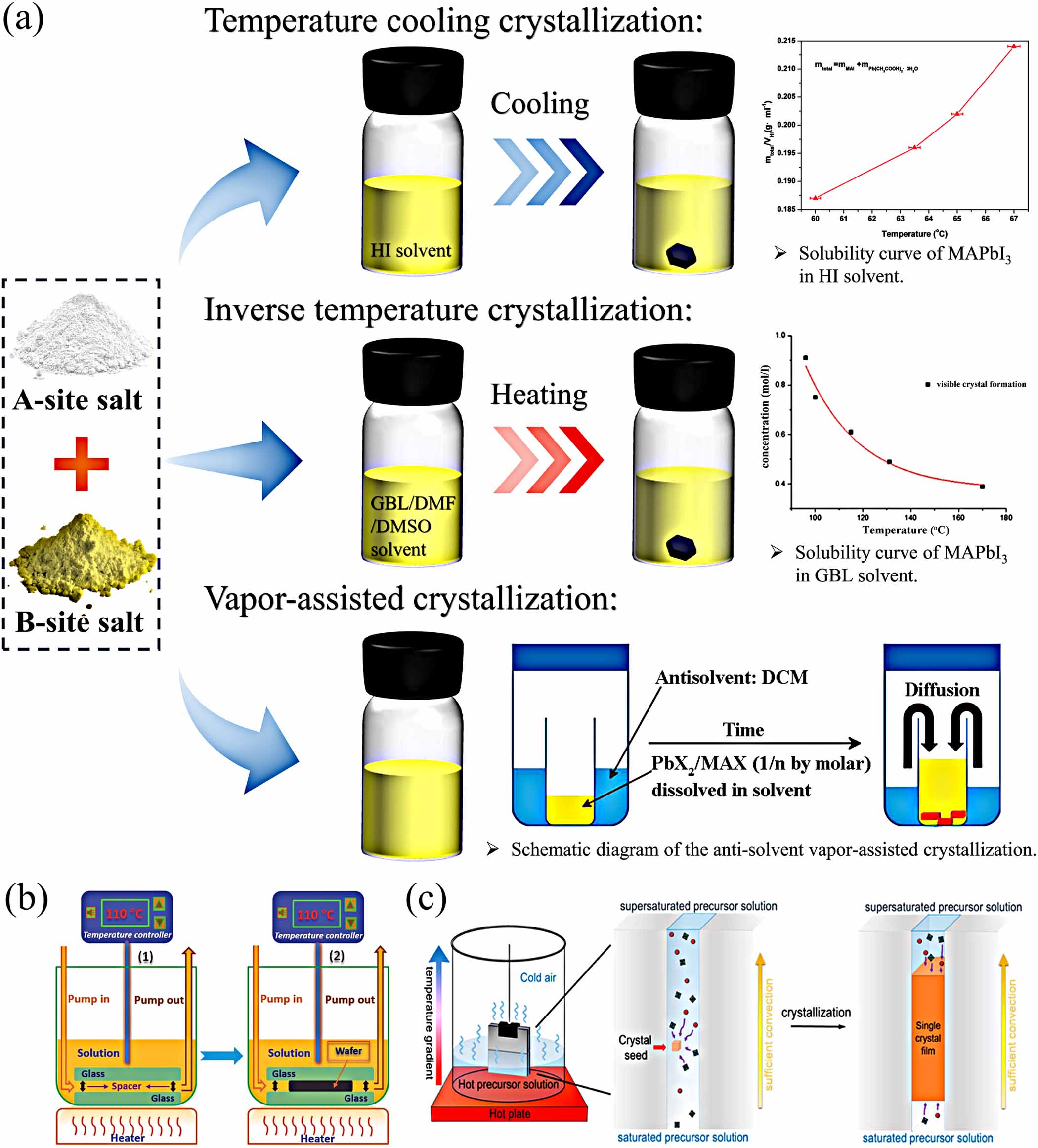
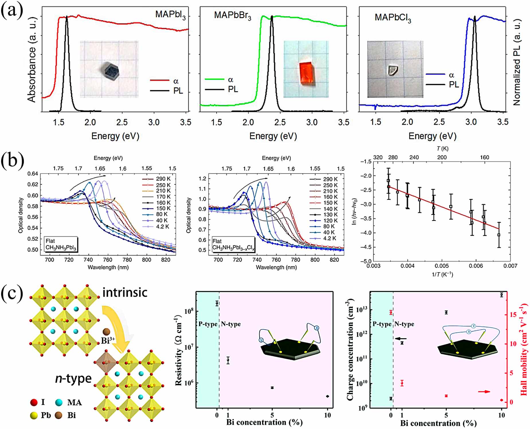
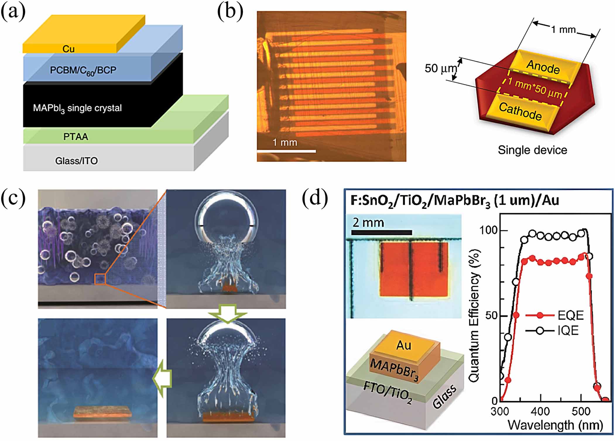
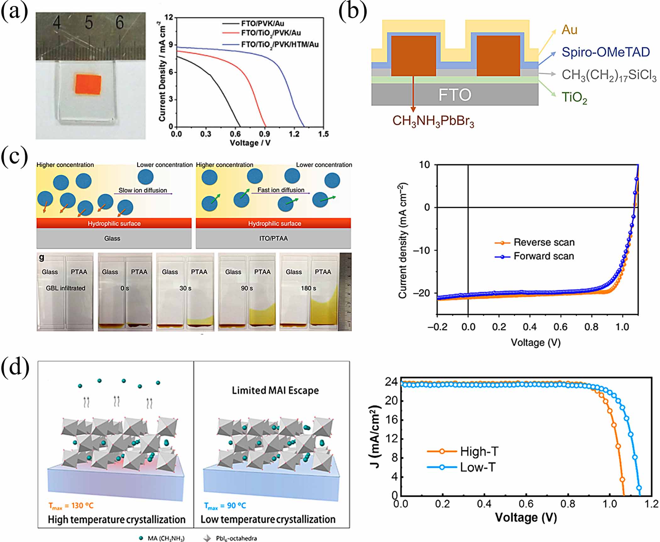
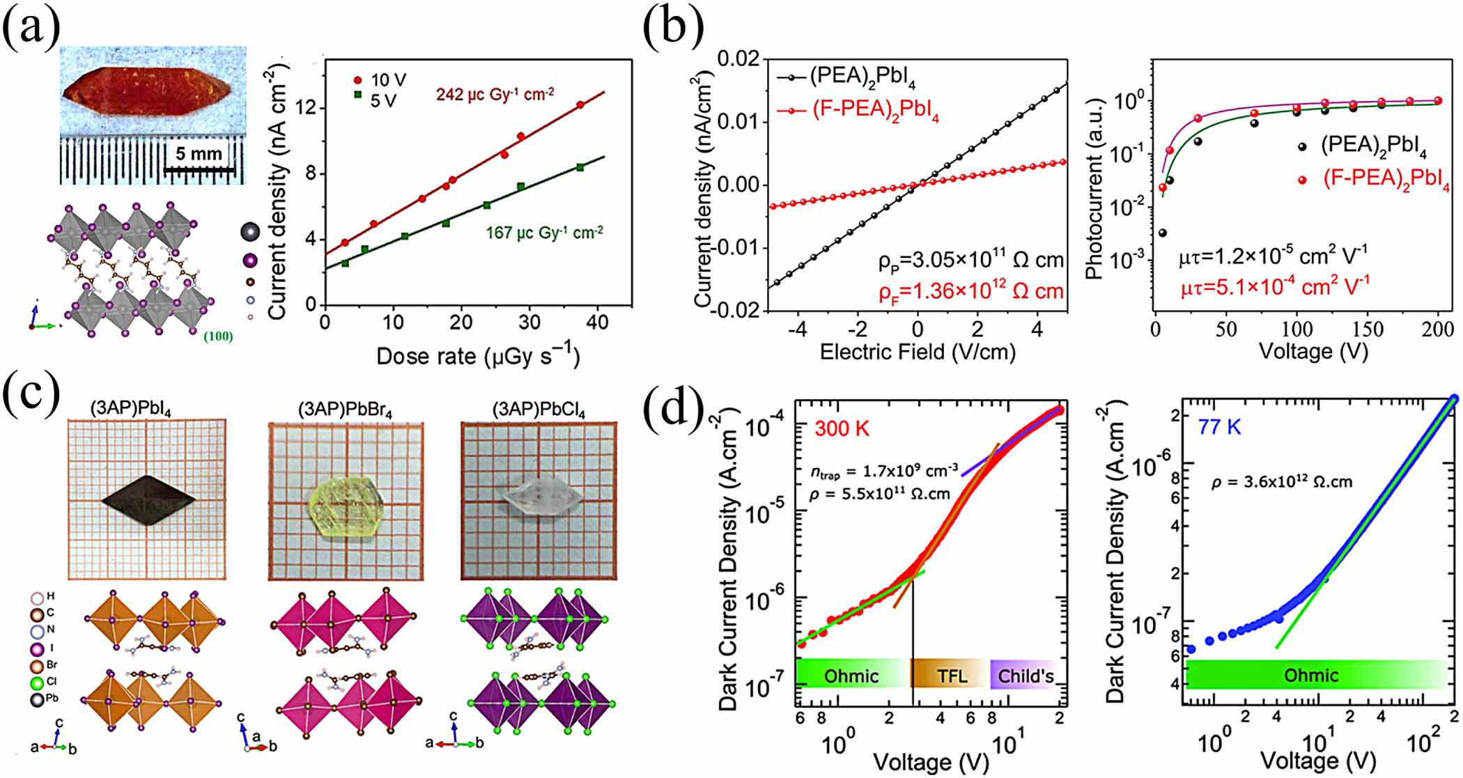
Figure 16. (a) Device architecture, and corresponding cross-sectional SEM image of CsPbBr3 nanocrystal-based LEDs. Reprinted with permission from [176]. Copyright (2020) American Chemical Society. (b) Schematic illustration of device fabrication process of the LIB method. Reprinted with permission from [177]. Copyright (2022) American Chemical Society. (c) Schematic of single crystal growth using a space-confined inverse-temperature crystallization method, and the LED performance of the corresponding device. Reproduced from [178], with permission from Springer Nature. (d) Lasing performance of the MAPbBr3 microcrystalline array. Reproduced from [179]. CC BY 4.0.
Download figure:
Standard image High-resolution image
Perovskite materials have achieved remarkable advances in the field of micro-lasers in recent years. By utilizing perovskite materials with various morphologies and structures, laser emission within the range of 420–825 nm can be realized. Perovskite micro-lasers can be classified into three major types based on optical resonator modes: whispering gallery modes (WGMs), Fabry–Pérot (F–P) modes, and random modes [173]. In 2015, Zhu et al reported a wavelength-tunable laser based on halide perovskite nanocrystals with an extremely low lasing thresholds (220 nJ cm−2) and a high-quality factor (Q∼3600) [16]. Time-resolved fluorescence kinetic analysis shows minimal charge carrier trapping in these single-crystal nanowires and achieves estimated lasing quantum yields near 100%, verifying that halide perovskite is a perfect lasing gain material. Recently, Pan et al fabricates large-area perovskite nanocrystal arrays with an area of 100 cm2 using spatial confinement and antisolvent-assisted crystallization, and the pixel size could be tuned from 2 μm to 8 μm [179]. The crystal pixel can serve as a high-quality WGM microcavity with a quality factor of 2915 and a threshold of 4.14 μJ cm−2, as shown in 15d. Despite the advances in optically pumped perovskite lasers, there is more interest in electrically pumped perovskite lasers that can attain high power, high stability and low threshold, which is the ultimate aim of perovskite lasers. To accomplish this aim, some challenges remain to be overcome, such as how to integrate EL devices with resonant cavities without compromising the charge carrier injection efficiency; and how to prevent carrier transporting layers in EL devices from adversely affecting the laser output.
7. Future perspectives
The optoelectronic device of perovskite single crystals has experienced rapid development during the past few years. In this review, we analyzed the intrinsic physical properties of perovskite single-crystal optoelectronic devices to explain their superior performance. First, perovskite single crystals have a strong light-harvesting capacity, allowing them to absorb more photons under light illumination. The electron-hole pairs generated by the absorbed photons dissociate more easily into free carriers because of the weak exciton binding in perovskite single crystals. Finally, the superior carrier transporting behavior of single crystals, such as long diffusion distance and low defect state, results in minimal carrier loss throughout the drifting process. Based on these advantages, we summarized the development of perovskite single-crystal optoelectronic devices, primarily solar cells, detectors and LEDs, over the past years. However, research on single-crystal device development lags significantly behind polycrystalline device research. For example, the PCE of single-crystal solar cells has a lower PCE than their polycrystalline counterparts. Future improvements in the application of perovskite single crystals must overcome the following issues.
7.1. Thickness control and substrate coupling of single crystals
Reducing the crystal thickness is crucial for carrier transport in perovskite single crystal optoelectronic devices based vertically structured. Previous studies have achieved several microns of crystal thickness by using space-confined and other growth methods, but this is still far beyond the penetration depth of visible light, which increases the carrier transport distance and the possibility of carrier loss. Therefore, it is essential to further develop the single crystal preparation process to obtain large-area, nanometer-thick single crystals. In addition, there are various interactions between perovskite single crystals and substrates, such as mechanical force and van der Waals force, which not only determine the growth and morphology of the single crystals, but also affect the contact quality between the single crystals and the substrates. By using pulsed laser deposition and atomic layer deposition techniques, high-quality and highly oriented single crystals can be epitaxially grown on specific substrates with close contact. The epitaxially grown has been extensively applied to 2D materials and conventional oxide perovskite materials, but remains underexplored in the field of hybrid perovskites.
7.2. The modification of the surface defect of perovskite single crystals
As reported, perovskite single crystals have a low trap density of ∼1010 cm−3, and their inherent properties are hindered by surface dangling bonds, dislocations, and chemical contamination. Many reports have confirmed that the surface recombination velocity of perovskite single crystals is higher than that of polycrystalline films by a factor of 6 [180]. In photoelectronic devices, significant carrier recombination will result in a performance decline, particularly in solar cells. It described why single-crystal solar cells have a lower PCE than their polycrystalline counterparts. The key to improving the performance of single-crystal electrical devices is reducing the surface imperfections of single crystals. Some researchers have developed new crystal growth techniques to eliminate surface vacancy defects, such as minimizing MA+/I− effusion by synthesizing at low temperatures. The surface passivation methods referred to by polycrystalline cells to suppress defect recombination should also be considered in parallel.
7.3. Interface modulation between of single crystal and transport layers
The record efficiency of polycrystalline PSCs has reached 26%, and the Voc of high-efficiency devices approach 1.20 V. However, the highest efficiency reported for single-crystal PSCs is only 22.8%. Single-crystals have lower bulk defects than polycrystalline films, but single-crystal PSCs show larger Voc loss when the perovskite layer with the same band gap. One of the factors that limit high Voc is the presence of crystal surface defects, and another important factor is the mismatch energy level alignment between perovskite single crystals and carrier transport layers. Many strategies have been developed to optimize the internal energy level arrangement in polycrystalline PSCs. For example, it has recently been reported to develop some self-assembled monolayer as the hole transport layer of the inverted PSCs. These materials not only achieve good energy-level alignment with the perovskite layer, but also improves the interfacial adhesion through covalent bonds. However, the application of self-assembled monolayer to the preparation of single-crystal PSCs has not been explored. To achieve higher PCE than polycrystalline PSCs, single-crystal PSCs must optimize carrier transit barrier and achieving the higher Voc of the devices.
7.4. Designing large-area, arraying photoelectronic devices
Large-area integrated manufacturing is as crucial for commercial applications as efficiency, stability, and cost for photoelectronic devices. According to different application requirements, device morphology needs to have different development directions. Solar cells need large effective area photovoltaic modules to enhance photon utilization. In photodetectors and LEDs, them need high resolution which requires smaller and more pixel unit devices per unit area. Perovskite single crystals have excellent uniformity, no grain boundaries and low defects, and can ensure the consistency and efficiency of each pixel unit device. However, the preparation of perovskite single crystals usually adopts the solution method, but this method is time-consuming and inefficient. Therefore, to achieve large-area array integrated devices, it is necessary to develop methods that can obtain large-volume single crystals and optimize the wafer processing technology, in order to achieve large-area wafer preparation comparable to silicon wafers.
7.5. Improving stability and developing encapsulation of devices
The stability of perovskite single crystal optoelectronic devices is crucial for their application development, but it is not the primary concern compared to the first four parts. Since the performance of single crystal devices is far from the optimal level, the stability improvement is also constrained. Stability is affected by various factors, such as thermal decomposition, ion migration, and degradation of metal electrodes within the device. In LEDs devices, reducing the Joule heat generated during operation can prevent the performance degradation caused by thermal decomposition. In addition, preventing devices from being eroded by environments, such as water and oxygen, is also essential for improving stability. In practical applications, encapsulation can effectively protect devices from the damage of air, which has been verified for polycrystalline devices. Based on the special structural of single crystal devices, developing new encapsulation techniques is a future direction.
Acknowledgments
This work was supported by the National Natural Science Foundation of China (52025028 and 52202273), the Natural Science Foundation of Jiangsu Province (BK20210728), and Funded by the Priority Academic Program Development (PAPD) of Jiangsu Higher Education Institutions.