
Abstract
Bottom-up fill of Cu in deep submicrometer via holes was achieved through electroless plating alone for the first time. We investigated the effect of addition of inhibitor molecules to electroless Cu plating solution, and found that sulfopropyl sulfonate (SPS) was highly effective in promoting the bottom-up fill. The tendency for bottom-up filling was enhanced by shrinkage of the hole diameter. This suggests that the diffusion flux of SPS molecules to the bottom of holes was more suppressed for smaller holes. Thus, the Cu deposition rate near the hole bottom is larger than that outside the hole, leading to bottom-up filling. © 2004 The Electrochemical Society. All rights reserved.
Export citation and abstract BibTeX RIS
Copper is used widely for metal interconnection in ultralarge scale integrated (ULSIs) owing to its low resistivity and high reliability against electromigration. The present damascene copper interconnections are fabricated by electroplating on a sputtered Cu seed layer.1 2 3 Bottom-up fill (also referred to as superfilling) of Cu using additives, such as sulfopropyl-sulfonate (SPS), aminobenzothiazole, benzotriazole, and 3-mercapto-1-propanesulfonate (MPSA), in an electroplating solution has been studied extensively.4 5 6 However, with the rapid shrinkage in interconnection dimensions, it is increasingly more difficult to form a continuous sputtered Cu seed layer on the sidewalls of fine via holes, which results in voiding during electroplating.7 Given the surface reaction dominated deposition mechanisms they involve, copper electroless plating and chemical vapor deposition (CVD) promise to yield conformal deposition profiles.8 9 10 11 12 Copper bottom-up fill with CVD using iodine as a catalyst was reported by Shim et al.12 Gandikota et al. and Andryuschenko and Reid reported the use of Cu electroless plating for repairing poor sidewall coverage induced by sputtered Cu.13 14 Recently, researchers found that displacement plating of Cu is possible on TaN after wet chemical etching of the native oxide, and that a good adhesion between Cu and TaN can be obtained.15 16 17 A continuous Cu film as thin as 10 nm may be deposited by electroless plating over a 1 nm thick Pd catalytic layer formed by ionized cluster beam (ICB) deposition, by which highly collimated ionized Pd clusters with diameter of a few nanometers may be obtained.18 They also found that the adhesion between the Cu film and TaN layer was as strong as that between sputtered Cu and TaN.19
This study aims to achieve the filling of submicrometer holes solely by controlling the additives in the electroless plating solution. While bottom-up deposition of Cu by electroplating with additives has been studied extensively, there have been only a few reports on bottom-up deposition by electroless plating. Lopatin and co-workers observed that thicker Cu film deposited at the bottom corner of submicrometer trenches rather than at the top opening when surfactant Tritton and RE 610 were added to an electroplating bath that used formaldehyde as a reducing agent.20 21
In this study, we first investigated the effect of inhibitors, such as SPS, benzotriazole, and thiourea, on the deposition rate obtained by electroless plating. Then, we found that the deposition rate of Cu was reduced by the addition of 0.5 mg/L of SPS or thiourea. However, bottom-up deposition was observed only in electroless plating using SPS. We also examined Cu deposition characteristics with various poly(ethylene glycol) (PEG) molecular weights between 4000 and 400, and observed the bottom-up deposition when the molecular weight was larger than 800.
Experimental
We used an ICB-Pd catalyst, a few nanometers thick, for catalyst as well as an adhesive layer. The electroless Cu plating bath typically contains  (6.4 g/L),
  (ethylenediaminetetraacetic acid, EDTA, 70.0 g/L), glyoxylic acid (18.0 g/L),22 polyethylene glycol (PEG, Mw 4000, 0.5 g/L), and tetramethylammonium hydroxide (TMAH) as a pH controller. The pH of the plating solution was adjusted to about 12.5, and the bath temperature was 70°C. Adhesion between the electroless plated Cu film and TaN barrier layer was characterized based on the peel strength. The specimens were cut by a focused ion beam (FIB) in preparation for cross-sectional scanning electron microscopy (SEM) and transmission electron microscopy (TEM). To protect Cu from etching during the FIB process, a carbon layer a few tens of nanometers thick was evaporated on the Cu-plated samples. Furthermore, a tungsten (W) layer was deposited on the sample surfaces by FIB-induced decomposition.
Results and Discussion
We examined the effect of SPS concentration on the bottom-up filling characteristics of a submicrometer hole whose diameter and depth were 0.4 and 2.3 μm, respectively. Figure 1 shows the bottom-up ratio, Tb/Ts, (Ts: Cu thickness at surface, Tb: Cu thickness at the bottom of the hole) of electroless plated Cu as a function of SPS concentration. The bottom-up ratio increased with SPS concentration. However, when the SPS concentration exceeded 1.5 mg/L, electroless deposition of Cu stopped due to excessive inhibition. Cu filling behavior was characterized for various diameter holes at an SPS concentration of 0.5 mg/L. Time dependence of the Cu deposition profile is shown in Fig. 2. Deposition rate of Cu at the substrate surface was greatly suppressed by the addition of SPS, however, because the effect was weaker at the hole bottom, the hole was filled from bottom to top (Fig. 2a and b). The holes were almost completely filled after 20 min as shown in Fig. 2c. We also found that the tendency for bottom-up filling decreased with increasing hole diameter. This is illustrated in Fig. 3, where the bottom-up ratio is plotted as a function of hole diameter. The bottom-up ratio increased by more than a factor of five as the hole diameter decreased from 1.0 to 0.3 μm. These results suggest that the time needed for complete filling is shorter for smaller diameter holes.
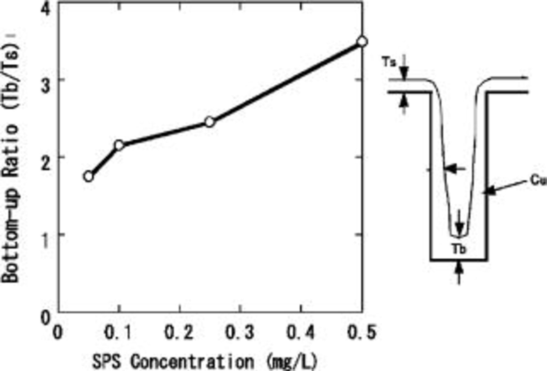
Figure 1. Bottom-up ratio of electroless plated Cu as a function of the SPS concentration. Hole diameter and depth were 0.4 and 2.3 μm, respectively. Deposition time was 4 min. Additives: SPS and PEG (molecular weight 4000; 0.5 g/L). pH 12.5; temperature: 70°C.
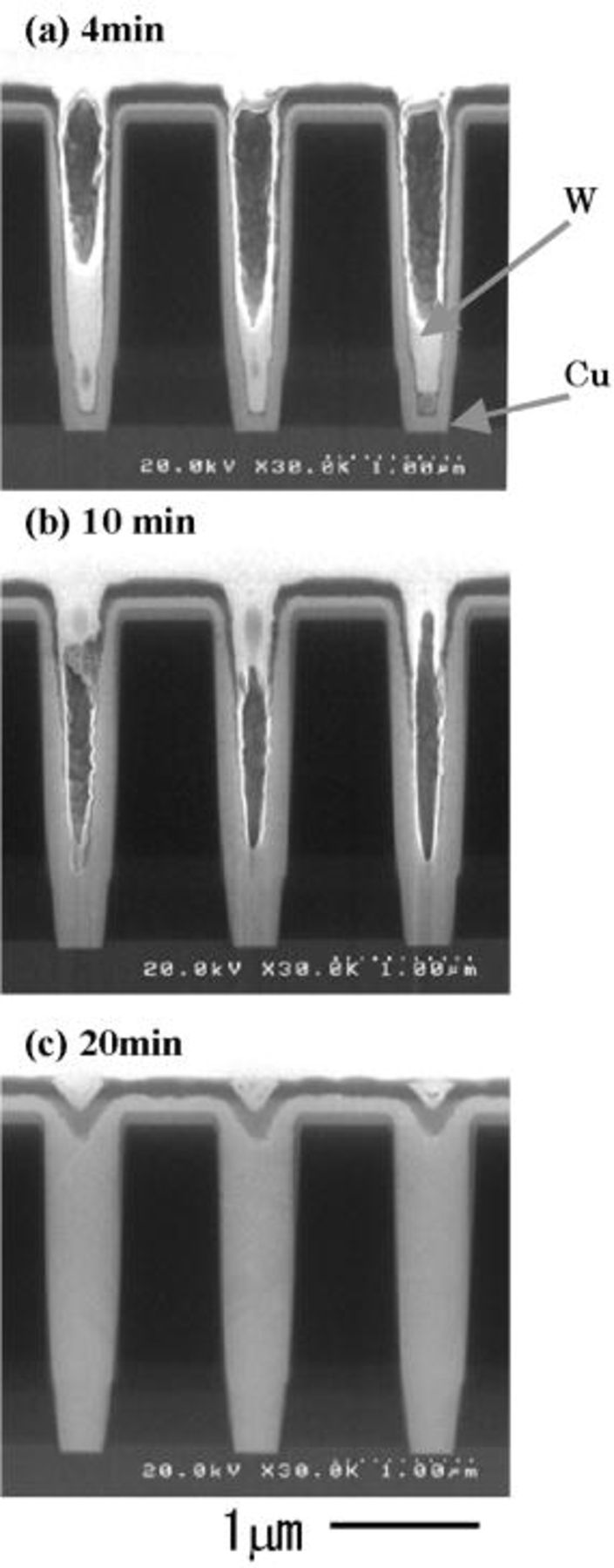
Figure 2. Cross-sectional SEM micrographs of electroless Cu deposition profiles for various plating times. Via hole diameter and depth were 0.4 and 2.3 μm. Additives: SPS (0.5 mg/L) and PEG (molecular weight 4000; 0.5 g/L). pH 12.5; temperature 70°C.
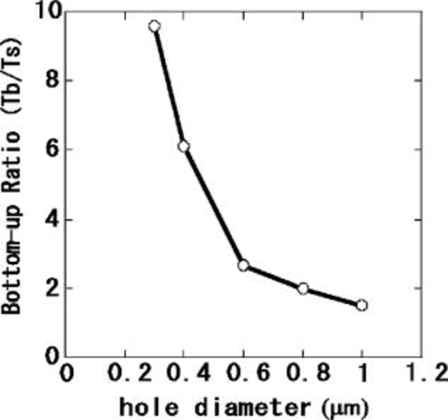
Figure 3. Diameter dependence of the bottom-up ratio of the electroless plated Cu. Via hole depth is 2.3 μm. Deposition time was 10 min. Additives: SPS (0.5 mg/L) and PEG (molecular weight 4000; 0.5 g/L). pH 12.5; temperature 70°C.
Finally, we succeeded in completely filling 100 nm diameter holes having an aspect ratio of 8 using electroless plating only, as shown in the cross-sectional TEM micrograph in Fig. 4. Remarkably, the Cu surface was flat after electroless plating, without any overgrowth that occurred in electroplating.23 24 There were no voids in the hole, and the Cu grain size was rather small, ranging from 10 to 50 nm.
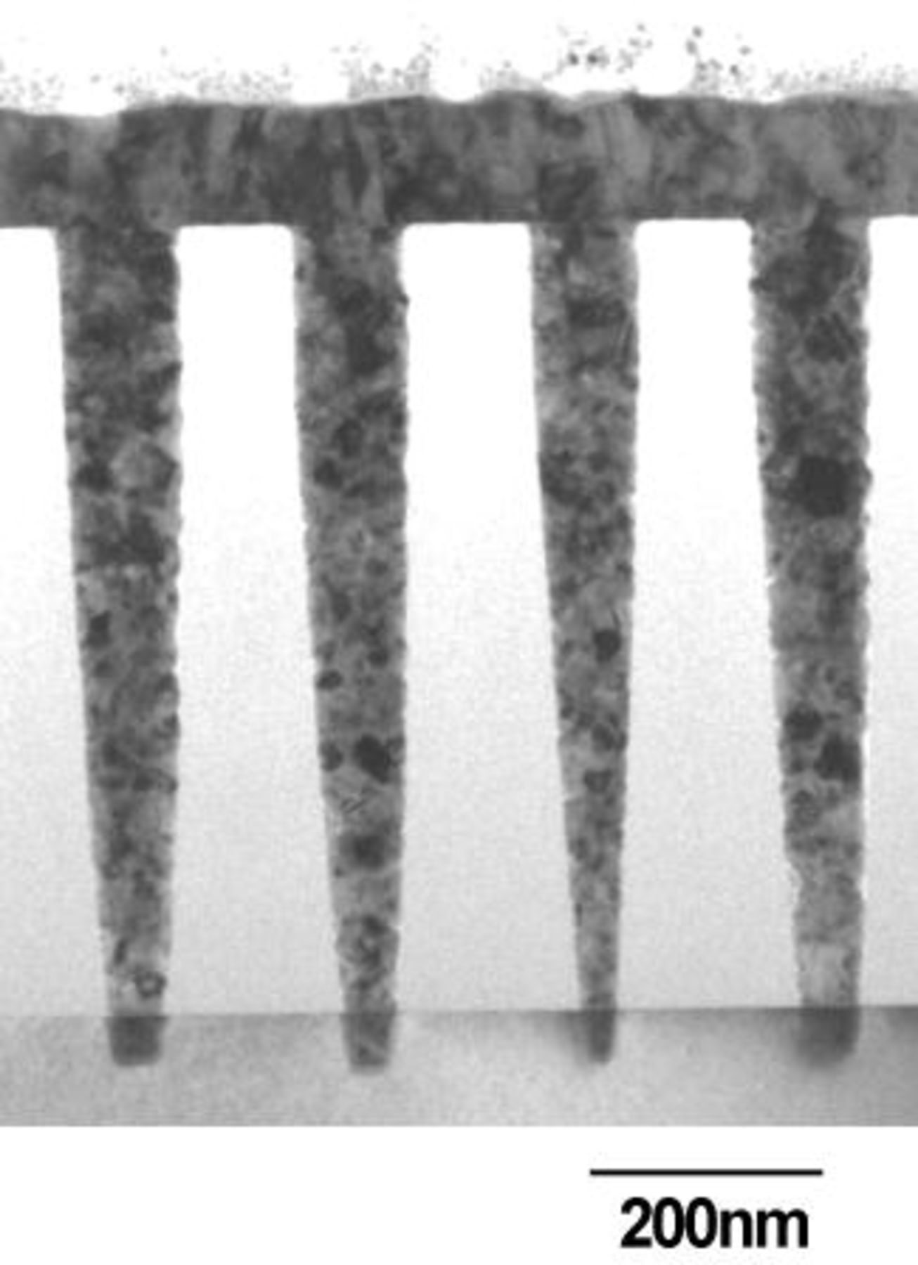
Figure 4. Cross-sectional TEM micrograph of a 100 nm via hole filled with electroless plated Cu. A 1 nm ICB-Pd catalyst layer was used. Deposition time: 2 min. Additives: SPS (0.5 mg/L) and PEG (molecular weight 4000; 0.5 g/L). pH 12.5; temperature 70°C.
For the bottom-up filling of electroplating of Cu, Moffat et al. , and West et al. proposed that surface curvature enhanced accelerator coverage (CEAC) mechanism was essential for determining bottom-up filling characteristics.25 26 Further, Moffat and Josell et al. incorporated the effects of electrical potential distribution and a gradient of cupric ion concentration in the via hole, and successfully reproduced superconformal filling characteristics by numerical simulation. Also, the CEAC model was able to explain bump formation by overgrowth after filling of holes.27 There is no potential distribution in electroless plating, and it would be better to investigate a much simpler situation. The bottom-up fill behavior observed in our experiments may be explained by the diffusion-controlled adsorption21 of inhibitor molecules (SPS) on the Cu surface. When adsorbed on the copper film surface, SPS reduces the active area of self-catalytic deposition of Cu, thereby reducing the Cu deposition rate. Because the concentration of SPS in the electroless plating solution is very low (0.5 mg/L), SPS is incorporated into the Cu film during deposition. Generally, the diffusion flux of inhibitor molecules decreases toward the hole bottom. The balance between the adsorption and incorporation rates determines the density of inhibitor molecules at the Cu surface. Because the adsorption rate is determined by the diffusion flux, a lower surface density of SPS results at the bottom of the hole relative to the top. Consequently, copper deposition proceeds more rapidly at the bottom than at the entrance of the hole or the surface outside the hole, leading to bottom-up filling. While they did act as inhibitors during electroless Cu deposition, bottom-up filling was not observed in thiourea and benzotriazole. This is presumably because these molecules have higher diffusion rates compared to SPS because of their smaller size (molecular weights of thiourea, benzotriazole, and SPS are 79, 119, and 304, respectively.).
Conclusions
We achieved bottom-up filling of Cu using electroless plating only.28 The technique involved the addition of SPS to the electroless Cu plating solution, along with the use of ultrathin ICB-Pd serving as both an adhesive layer and a catalyst for electroless Cu plating. Bottom-up filling yielded a flattened Cu surface, believed to be due to the high adsorption rate of SPS molecules on the flat surface. This simplifies the subsequent chemical mechanical polishing (CMP) process. The present technique promises to replace conventional Cu electroplating technology that uses a sputtered Cu seed.
Acknowledgment
The authors express their gratitude for the partial financial support provided by grant-in-aid no. 13025233 of the Japanese ministry of education, culture, sports, science, and technology.
Dr. Shingubara assisted in meeting the publication costs of this article.