
Abstract
The most important advantage of a source-gated transistor compared with a field-effect transistor (FET) is its low saturation voltage and high output impedance. Here we model a reverse biased gated Schottky barrier source in hydrogenated amorphous silicon and show good qualitative agreement between the calculated effect of source geometry and measurements. Furthermore, calculations of electron concentration profiles in the source show why the source-gated transistor in hydrogenated amorphous silicon is more stable than an equivalent FET.
Export citation and abstract BibTeX RIS
A new form of thin-film transistors (TFT) was introduced recently called the source gated transistor (SGT).1 The basic principle of operation is different from a conventional field-effect transistor (FET) where the electrical field induced by the gate modulates the channel conductance and current saturates when the semiconductor region at the drain end is depleted.
In the SGT, the electric field induced by a gate located directly below the source is used to change the current through a reverse biased source barrier and current saturates when the semiconductor underneath the source barrier is depleted by the reverse biased barrier. Figure 1 shows a schematic drawing of the SGT transistor. The electron current flows from the source barrier to the semiconductor-insulator interface and then laterally to the drain contact.
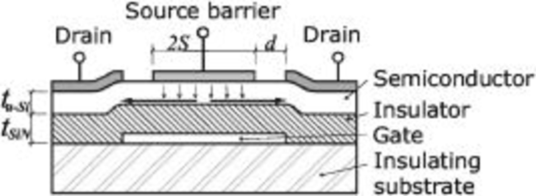
Figure 1. Schematic drawing of SGT transistor. The gap between source and drain contacts is defined as the source-drain separation  .
.
The SGT has many advantages over a conventional FET such as excellent output characteristics with low saturation voltage and very high output impedance.2 An example is shown in Fig. 2. Moreover, the SGT in hydrogenated amorphous silicon  shows good device stability at low currents,3 which allows us to consider these devices for analog circuits. Short channel effects are also reduced in the SGT.4 Furthermore, it has been shown that a useful dynamic range can be achieved by increasing the capacitance of the gate dielectric.5
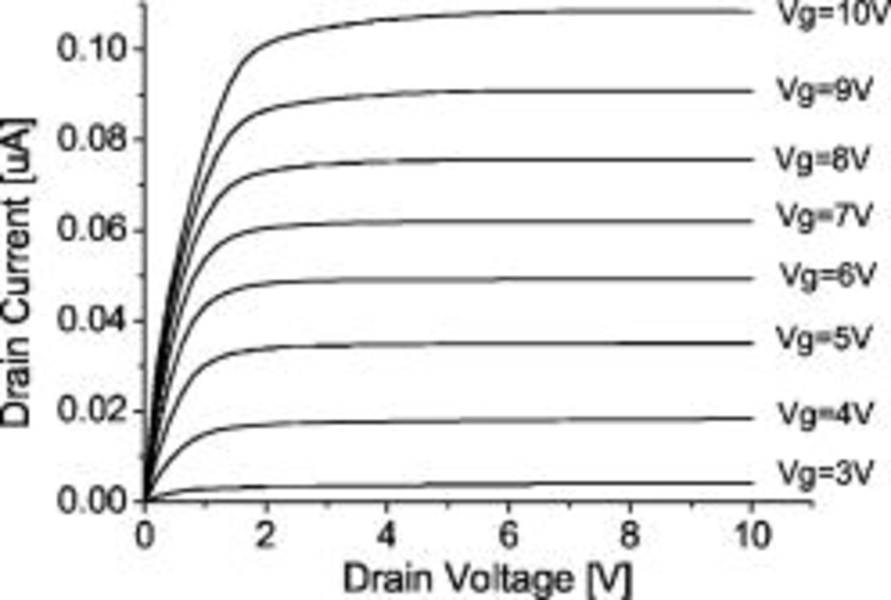
Figure 2. Experimental SGT transistor characteristics. The width of the device and source-drain separation was 12 and  , respectively (
 and
and  ).
).
SGTs have been made in  using a Schottky barrier source and ion implantation technology to control the effective source barrier height and passivate the region between the source and drain contacts (see Fig. 1). The gate insulator was silicon nitride. The gate was extended under the region
  to form a parasitic FET in series with the source barrier. This is necessary in
  , otherwise its high resistivity would introduce an unacceptably high parasitic drain resistance in the on state. In this configuration, the on state is controlled by the gated source barrier while the off state is controlled by the parasitic FET.6
The modeling of SGT structures has some commonality with modeling of specific types of organic FET structures where source and drain contacts are placed on the top of the organic layer.7 Although the objective in this case is to make ohmic contacts for good FET performance, the effect of distributed trap states and different source/drain work functions have been investigated and it has been shown that a variety of interesting peculiarities can occur in the FET characteristics including a sharp transition into the saturation region and low gate dependence on the current. These results form an ohmic resistance of the organic semiconductor between source/drain and the channel of the FET. A paper on the modeling of the SGT in amorphous silicon based on ISE-TCAD DESSIS also explains the sharp saturation and large reduction in current in some structures based on a large resistance in the source region that restricts the current.8
The gated source barrier is a vital part of the SGT concept since it controls the on state. A full understanding of the behavior of the source barrier is necessary, therefore, in order to characterize these devices. Here we are reporting on the source modeling of the SGT in  , based on Silvaco ATLAS. In particular, how the barrier height and geometry of the source influence device performance is compared with experiment. These issues are related to the validity of the dielectric model2 for the saturation voltage and the stability of the SGT. It is shown by comparing modeling with experimental results that the source current in our case, in contrast with Ref. 8, is controlled by the source barrier and its field dependence.
Comparison of Modeling with Experiment
Modeling of the SGT was done using the developer version of the Silvaco ATLAS (v.5.7.28.C) program with the latest implementation of the model for the barrier tunneling and lowering mechanism.9, 10 In the experimental work, the source Schottky barrier height was modified using a phosphorus implantation to increase the surface field and raise the source current by thermionic-field emission. However, in the model an effective Schottky barrier height was used and the electric field was simply that induced by the gate with no built-in field due to the implant. In this simulation, the field was low and most of the barrier changes were due to image-force corrections.
The main parameters are specified in Table I.  is the barrier height, α the barrier lowering coefficient, and
  the tunneling effective mass for electrons.11 It is assumed that the total density of states in amorphous silicon (10% hydrogen content) is composed of four bands: two exponential tail bands [a donorlike valence band
  and an acceptorlike conduction band
  ] and two deep level bands [one acceptorlike
  and the other donorlike
  ], which are modeled using a Gaussian distribution. The values for these concentrations and corresponding decay constants
  are summarized in Table I.12–14 Mobility in extended states, which is different from field-effect mobility, for electrons and holes was taken from Ref. 12, 13. Next the values for
  bandgap
  and dielectric constant
  are also shown in Table I. For the rest of the amorphous silicon parameters (such as surface recombination velocity, electron affinity, effective density of states), the ATLAS default values were used.9 In the case of the silicon nitride insulating layer, all values were default values apart from the dielectric constant of
  .
.
Table I. Parameters used in the simulations.
| Parameter | Value | Unit |
|---|---|---|

| 0.4–0.6 | eV |

| 0.1 | — |
| α | 4 | nm |

|

|
 
|

| 0.025 | eV |

|

|
 
|

| 0.05 | eV |

|

|
 
|

| 0.1 | eV |

|

|
 
|

| 0.1 | eV |

| 15 |

|

| 0.5 |

|

| 1.8 | eV |

| 11.7 | — |

| 6.5 | — |
Simulation of the saturation voltage and its dependence on the source-drain separation  of the parasitic FET is shown in Fig. 3a. It is seen that for small
  when there is no constriction of the current, the slope of the curve is given very well by the dielectric model2 where the semiconductor is assumed to be depleted of charge at saturation and the slope
  is
is  , where
  and
and  are the semiconductor and insulator capacitances per unit area. For the structure shown in Fig. 1 (
 and
and  ), this calculated value is 0.155. As
  , increases the saturation voltage increases because voltage is dropped across the parasitic FET.6 It is seen that the change of saturation voltage with gate voltage can be ten times lower than a conventional FET
  . Similar trends are seen in the experimental results shown in Fig. 3b, which shows that the Atlas model is able to predict the saturation voltage for a given geometry.

Figure 3. Dependence of saturation voltage on gate source voltage for various source-drain separation  (a) modeled and (b) measured.
The current  through the SGT is determined by a reverse biased source barrier, i.e., it mainly depends on
  and its field dependence and area of the source. It has been shown that
  scales linearly with the source width but is independent of source-drain separation
  .4 In the case of source length
  (Fig. 1), the
  increases linearly with
  for high
  , however for lower
  the current has a tendency to saturate with increasing source length
  (Fig. 4a).
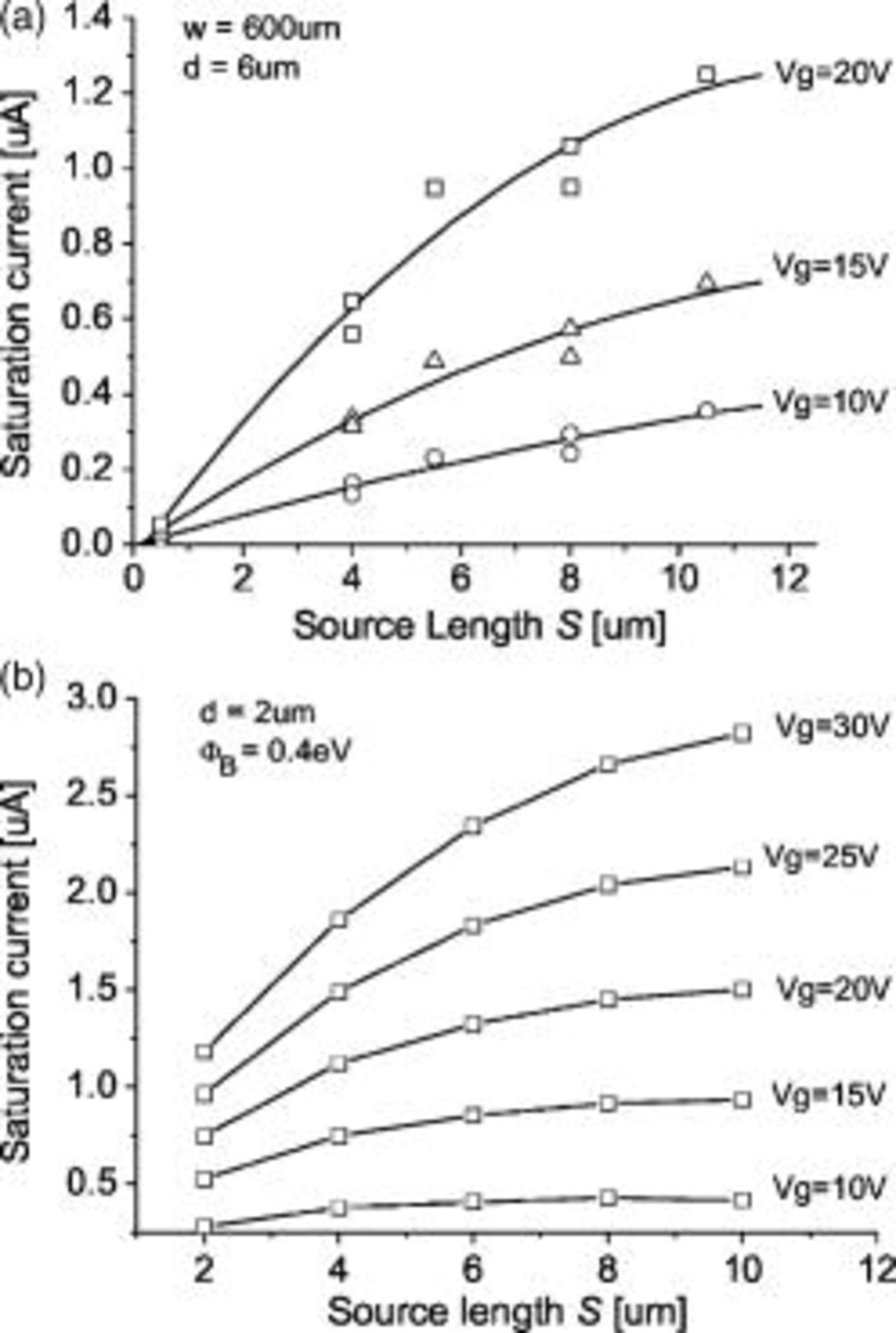
Figure 4. (a) Experimental and (b) simulated dependence of the saturation current on source length  .
.
The dependence of current on source length  calculated using Silvaco ATLAS is shown in Fig. 4b. It is seen that the change of the current with source length is in reasonable agreement with experiment (Fig. 4a). With low barriers and high currents, the source current tends to saturate with increasing source length.
The reason why the current tends to saturate can be seen with reference to Fig. 5, where the current density normal to the Schottky barrier interface is calculated. It is seen that for higher current passing across the interface (Fig. 5a), the current density is not uniform and is more concentrated towards the edge of the source opposite the drain contact. As the current through the source increases, there is a lateral voltage drop under the source barrier (Fig. 6a) and a large electric field gradient away from the edge of the source, and as the source length is increased, a smaller fraction of current per unit source length is added to the source current. With low currents, however, the lateral voltage drop is much smaller and there is a fairly uniform current density along the source giving a linear dependence between source current and source length  (Fig. 5b).
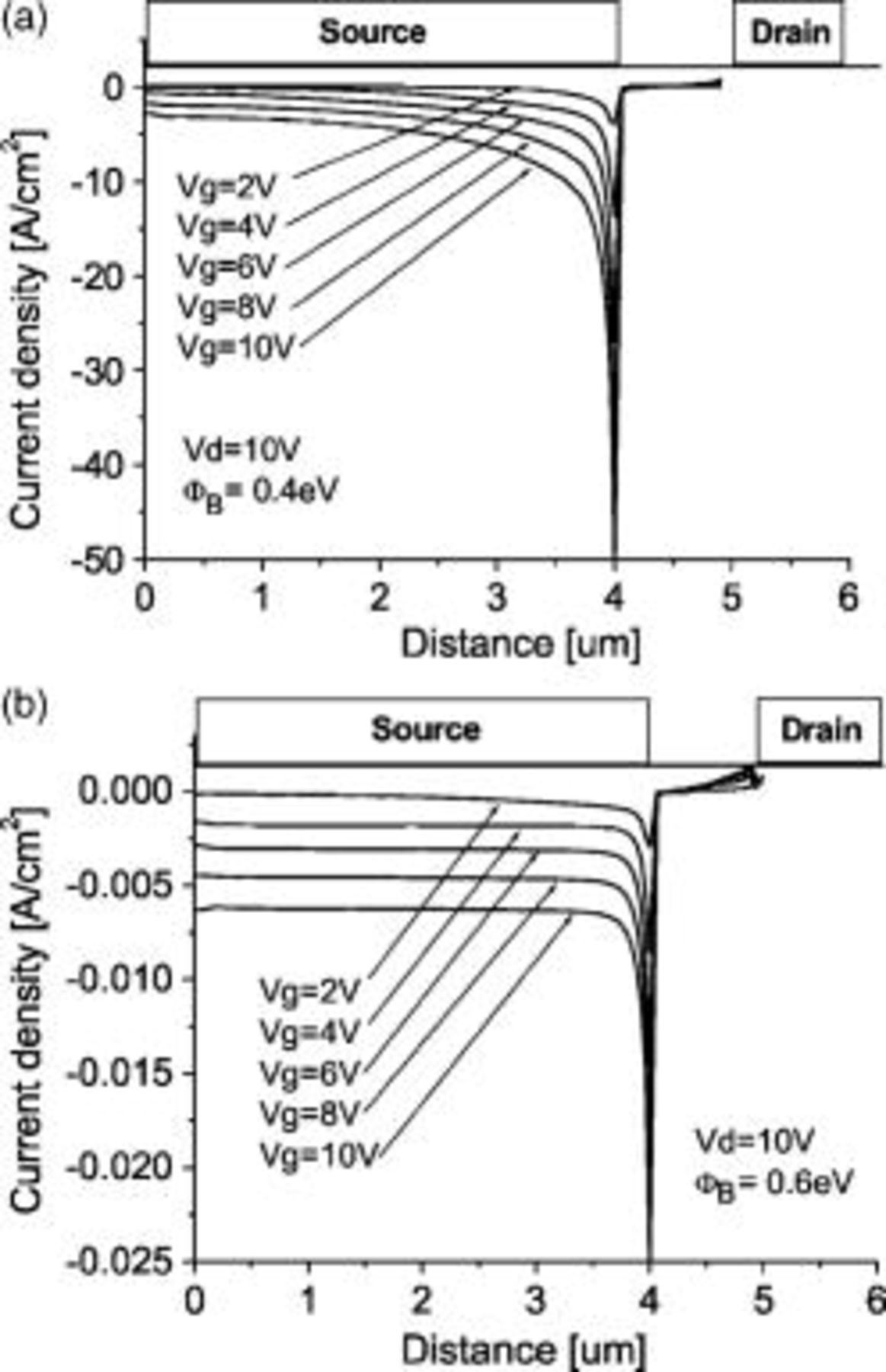
Figure 5. The calculated current density distribution along the source normal to the interface for two different barrier heights (a) 0.4 and (b)  .
.
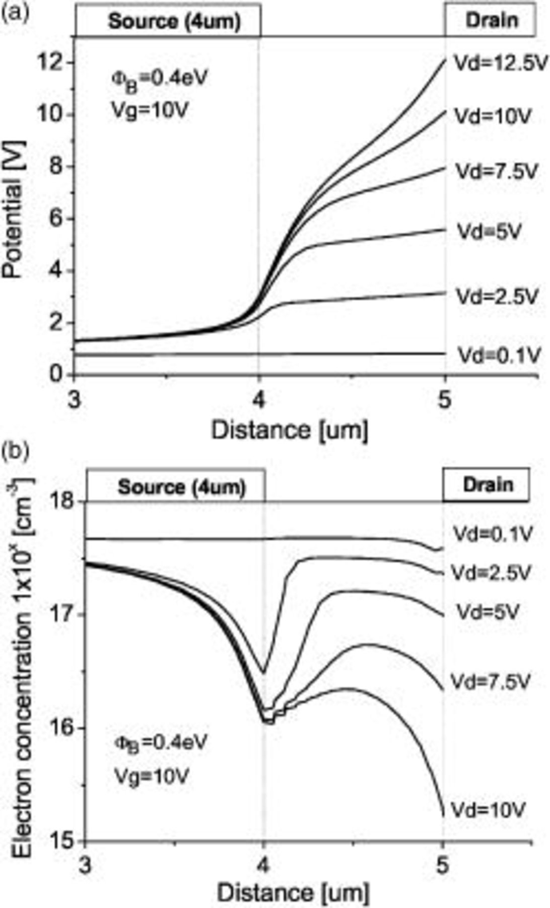
Figure 6. (a) Potential and (b) electron concentration distribution along the semiconductor-insulator interface under the source.
The feature of current crowding towards the edge of the source at high currents is further emphasized from the potential and electron concentration profiles along the semiconductor-insulator interface shown in Fig. 6. Here we also include the parasitic FET with a channel length of  .
.
The potential profile shows the lateral potential gradient under the source. When  is above the saturation voltage
  , the source depletion layer extends into the channel of the parasitic FET. At low drain voltages, the potential drop across the FET is negligible while the source potential of the FET floats upward to a value relative to the drain potential such that it just carries the saturation current supplied by the source barrier. When
  , which is around
  in this case, the device pinches off at the drain and the parasitic FET also operates in saturation and becomes depleted. This situation at large biased drain biases leads to further improvements to the output impedance.
For an FET biased into the on state, there is a large increase in the electron concentration and the electron quasi-Fermi-level moves toward the conduction band in the channel region. This is consequently accompanied by a rise in the generation of defect states (i.e., silicon dangling bonds) as the material strives to reach a new chemical equilibrium. These defect states trap electrons and cause a threshold voltage shift and current instability of the FET. However, in a low current SGT the region underneath the source barrier is depleted after current saturation so the quasi-Fermi level is closer to the thermal equilibrium state and the change between the off state and on state is smaller. Therefore, fewer states are generated in the  and the device is much more stable.3 The smaller excursion of the quasi-Fermi level in the SGT and the resultant reduction in defect generation and carrier trapping is a feature that can be usefully applied to many disordered semiconductors.
Interestingly for high current devices when the depletion under the source barrier is very nonuniform, most of the current flows in the region where the electron concentration is lowest and the device most stable. In Fig. 6, for example, the peak current density occurs where the electron concentration at the interface is  . This concentration has to be compared to the electron concentration of about
  at
at  from the source edge under the source contact. The amount of depletion is illustrated further in Fig. 7 where electron concentration profiles across the
  from the source barrier to the semiconductor-insulator interface are plotted and compared with a FET having the same layers. Clearly the electron concentration near the interface increases with the lower barrier and higher current device, but when a drain bias is applied it is still much lower than that in the FET. Therefore, as shown by experiment the SGT under a drain bias sufficient to deplete the
  is much more stable than an FET.3 However, this stability improvement is less at higher current levels (i.e., lower barrier heights), as can be seen by comparing the electron concentration
  and
and  . As pointed out by Lindner et al. ,8 the dielectric model is an approximation to the actual situation since it assumes no free electrons in the
  . These modeling results suggest that as one might expect, this approximation is good at low currents but gets worse as the barrier height reduces and the drain current increases.
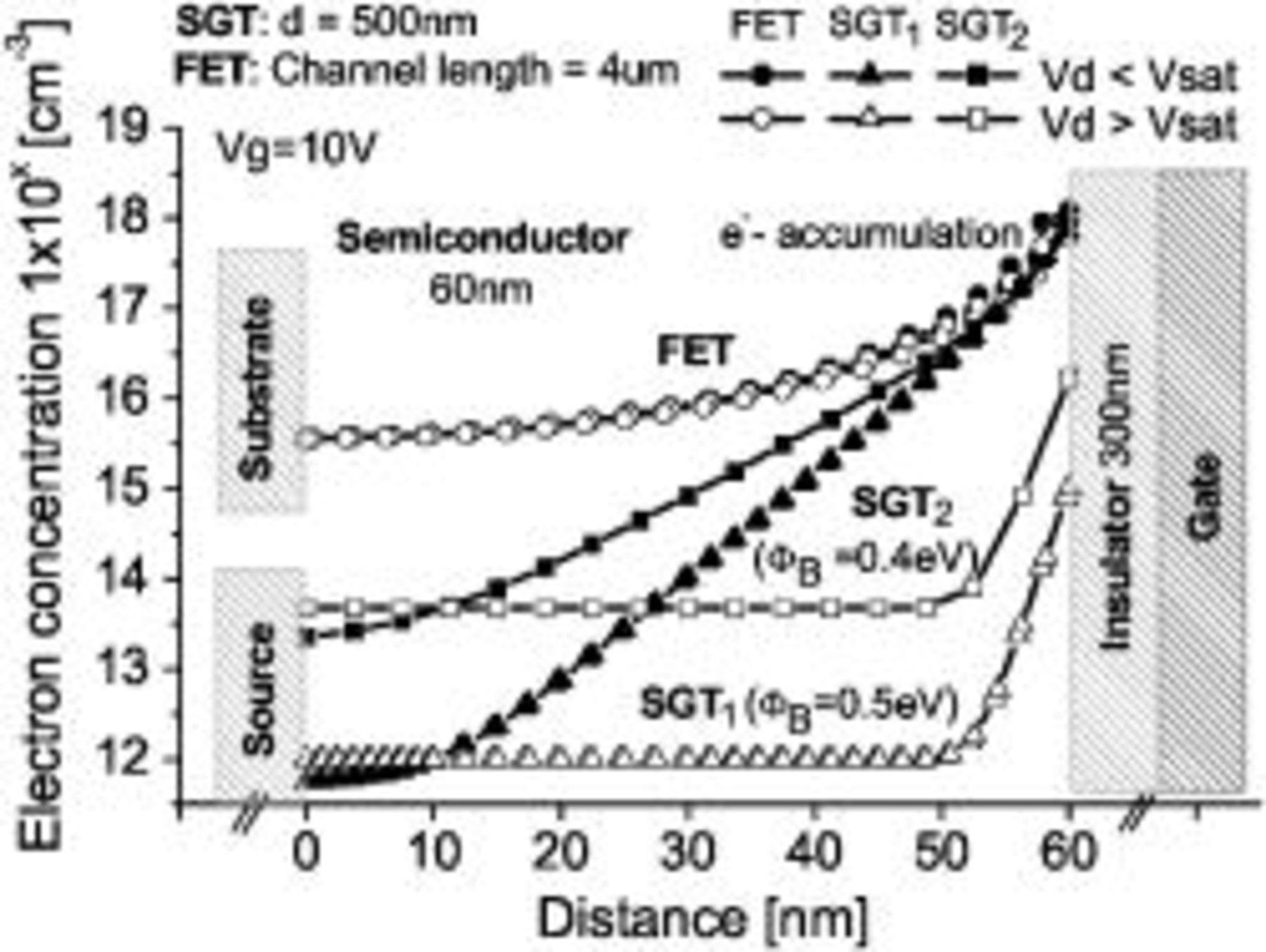
Figure 7. Electron concentration underneath the edge of the source barrier of a SGT with  and
and  . Also shown is the electron concentration
  from the source region of a FET. When
  , the current saturates and the
  layer in the SGT structure is depleted. In this condition, the electron concentration in the SGT is much lower than it is in the FET.
Conclusions
It has been shown that there is good qualitative agreement between experimental results and simulations using the Silvaco ATLAS program. The current is found to be dependent on the barrier height at the source and the on state controlled by the two-dimensional field distribution under the source barrier. This leads to the nonlinear dependence between device current and source length. The electron concentration under the source in saturation is much less that that in an equivalent FET. This leads to a smaller change in the quasi-Fermi level between equilibrium and the on state giving a reduction in defect generation rate and an increase in stability. This improvement in stability, however, can only be achieved when a drain bias is applied sufficient to deplete the  layer.
It is expected that these features of the SGT in amorphous silicon will be equally applicable to other disordered materials such as polymers. The reduction in the excursion of the quasi-Fermi level could be particularly important in materials where defect generation rate and carrier trapping are an issue.
Acknowledgments
This project is supported by Philips Research Laboratories Redhill and EPSRC Swindon, U.K.
University of Surrey assisted in meeting the publication costs of this article.