
Abstract
The high-temperature stability of lanthanum silicate gate dielectric metal-insulator-semiconductor (MIS) devices with either Ta or  electrodes has been studied. After a
  ,
,  rapid thermal annealing (RTA) treatment, devices with Ta gate metal undergo an equivalent oxide thickness (EOT) increase from 0.62 to
  or higher, while devices with
  as the gate electrode experience an EOT increase from 0.62 to only
  . An EOT less than
  is achieved after a
 RTA, with a corresponding gate leakage of
  . Medium-energy ion scattering and X-ray diffraction (XRD) analysis reveal that the Ta gate metal undergoes a phase change due to reaction with
  above
above  , while for
  no change in the XRD spectrum is detected. Interface state defect densities and leakage currents are reduced after the high-temperature processing. Results reveal the importance of the entire gate stack design and processing in obtaining good device properties.
Export citation and abstract BibTeX RIS
Lanthanum silicate holds potential as a high-κ gate dielectric for advanced metal-oxide-semiconductor field-effect-transistor (MOSFET) devices due to its properties of good dielectric constant  1 and an expected large band offset with respect to Si, based on that of
 .2 Lanthanum silicate is known to be much less reactive with the ambient environment than lanthana3 and has a higher temperature stability of the amorphous phase than lanthana.1 The reactivity of lanthana with silica to produce a silicate4, 5 provides a means of eliminating interface silica from metal-insulator-semiconductor (MIS) devices, thus offering a pathway towards achieving
  equivalent oxide thickness (EOT) devices under controlled processing conditions.6 Elsewhere we discuss the reaction between thin chemical oxide and lanthana to achieve very low EOT lanthanum silicate gate dielectric with no
  interface
  under low-temperature processing, characterized using high-resolution cross-sectional transmission electron microscopy (HRTEM), medium-energy ion-scattering (MEIS), and electrically using MIS devices.6 Other reports of sub-nm EOT MIS devices fabricated with lanthana or lanthanum silicate typically utilize gate electrodes such as Al or Au,7, 8 which cannot withstand high temperatures. Standard MOSFET device processing flows require the gate stack to be stable after an implant-activation rapid thermal anneal (RTA), at temperatures as high as
 . Thus, it is important to optimize the entire gate stack in terms of material compatibility and processing.
To better understand the issues concerning the thermal stability of lanthanum silicate dielectrics on Si, we have investigated the properties of sub-nm EOT MIS devices having either Ta or  gate electrodes, in an attempt to distinguish Si–dielectric reaction effects from dielectric–electrode reactions. Tantalum has several properties making it useful as a gate electrode for the study of high-κ gate dielectrics subject to high-temperature device processing conditions: simplicity in processing being an element rather than an alloy, a high melting point, thermodynamic stability (against oxide formation) in contact with lanthana,9 a favorable work function for n-MOS devices
  ,10 and the ability to be effectively etched using plasma processing. However, Ta is known to react at high temperature in contact with
  ,11, 12 and thus may not be stable in contact with lanthanum silicate. Stoichiometric
  , however, is expected to be stable in contact with
  11 and has been demonstrated to be a good electrode candidate for use with
  13 and with high-κ dielectrics.14 Thus, we compare the compatibility of these two gate metal candidates with lanthanum silicate gate dielectric.
Gate stack characterization has been performed using capacitance–voltage (C–V) and gate leakage (I–V) measurements of MIS devices, X-ray diffraction (XRD) analysis of the gate electrode structure, and MEIS to determine compositional profiles in the dielectric layer specifically for devices without electrodes.
Experimental
Using an ultrahigh vacuum (UHV) molecular beam epitaxy (MBE) system designed for deposition over  wafers, we have fabricated MIS devices by reactive evaporation of lanthanum in an oxygen ambient, on n-type Sb-doped
 substrates. Lanthanum silicate films were obtained by lanthana deposition on a silica chemical oxide formed by the SC2 step (5
  :1
:1  :1
:1  , for
, for  at
at  ) of an RCA clean, with an in situ reaction anneal of 400°C for
  in
in 
 to produce lanthanum silicate.6 Typical deposition conditions are
  in
in 
 , with a deposition rate
  . To minimize atmospheric reaction effects, a subsequent in situ E-beam deposition of a
  Ta gate is performed at
  , followed by an ex situ
  capping layer.
  gate electrode
  is deposited at ambient temperature in a UHV radio frequency (rf) magnetron sputtering system, under conditions of 100 W, in a
 mixture, as described elsewhere.15 This requires ex situ transfer, exposing the lanthanum silicate to air for about
  . The
. The  is also W-capped to give low contact resistance for good probe contact during electrical measurements. MIS devices are formed by patterning the top electrode using standard photolithographic processing and dry etching in an
  mixture.16 We have found this etch to be effective for both
  and Ta. Tungsten is sputter-deposited on the back of the Si substrate to obtain low contact resistance for electrical measurements.
To examine the high-temperature stability of the gate stacks, postprocess rapid thermal anneals (RTAs) were performed using an AG Associates Heat-Pulse 210. Processing was performed in flowing nitrogen or forming gas (1%  in
in  ) at temperatures ranging from 400–1000°C, typically for
  . Note that the heating rate for the RTA is about 60–90°C/s, so the total thermal budget is significantly longer than the programmed hold time indicates.
Electrical testing of capacitance and gate leakage characteristics has been performed using an HP 4192A impedance analyzer and HP 4145A semiconductor parameter analyzer probe stations. Device parameters such as the EOT and flatband voltage  have been extracted from the C–V data using the NCSU CVC modeling program.17 Capacitor sizes range from
  to
to  areas, measured at frequencies from
  to
to  , as is indicated.
Materials characterization has been performed using both XRD and MEIS. A Bruker AXS D-5000 diffractometer equipped with a large-area detector was used, operated with  radiation (
 ,
,  ). MEIS experiments were performed at Rutgers University18 with
 beams using a double alignment geometry in the (110) scattering plane, in which the incoming beam is aligned with the Si [100] channeling direction and the detector axis is aligned with the
  crystallographic axis. Details are described elsewhere.6, 19, 20 Depth profiles of the elements were obtained from simulations of the backscattered ion energy distribution, using layer densities extrapolated from bulk values (thus a thickness uncertainty exists). Quantitative depth profiles for different species can be extracted with a resolution as high as
  in the near-surface region; however, the depth resolution deteriorates for deeper layers20 due to the statistical nature of the ion–solid interaction. For enhanced resolution of the lanthanum silicate dielectric layer, some samples analyzed by MEIS had no gate electrode capping. Thus, these films had been exposed to air for a number of days before the MEIS measurement. All samples analyzed by MEIS experienced an in situ silicate reaction anneal of 500°C for
  .
.
Device Properties with Ta Gate Electrodes
For devices having E-beam evaporated Ta electrodes (resistivity of  as measured by 4-pt probe) the effects of high-temperature postprocess anneals on
  W/
W/ Ta/
Ta/ lanthanum silicate /
 gate stacks was studied. C–V characteristics are shown in Fig. 1, after
  RTA treatments in
  . The data are indicated by points, while lines are fits to the data using the NCSU CVC program17
,including quantum correction. Capacitor sizes are
. The data are indicated by points, while lines are fits to the data using the NCSU CVC program17
,including quantum correction. Capacitor sizes are  , measured at
  . For the lowest EOT films, it is difficult to obtain good C–V curves at frequencies lower than hundreds of kHz due to high leakage current. The observed "hump" in the curves near the threshold voltage indicates a high density of interface states,21 which decreases with increasing RTA temperature.
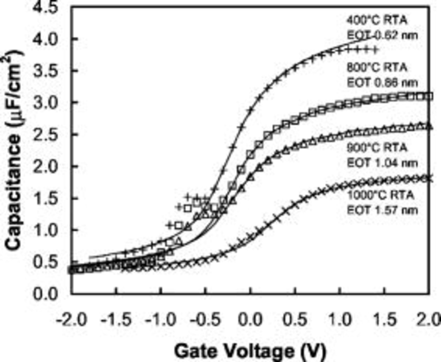
Figure 1. C–V properties of MIS devices with Ta gate electrodes, after RTA treatments from  for
for  in
in  . Measurement frequency is
  and capacitor size is
  . Lines are fit to the data using the NCSU CVC program.
With only low-temperature processing ( in situ reaction anneal,
  Ta deposition temperature, gate stack
  RTA in
  ,
,  ), devices having an EOT as low as
  are shown. For the low-temperature-processed case
  , EOT values in the range of 0.5–
 are typical, although the cause of EOT variation for different samples with nominally identical processing is uncertain. These EOT values are among the best reported for any MIS devices.6, 8 Forming gas anneals (FGAs) at
  for
for  lower fixed charge densities somewhat; however, FGA effects are not focused on in this report.
The observed decrease in accumulation capacitance (increase in EOT from 0.62 to  ) with increased processing temperature indicates that a gate-stack reaction occurs. Further evidence of interface reaction is the shift in
  and reduction of interface state density (with peak
  dropping from
  to
to  ) after the
  RTA. The flatband shift is more than expected due to merely a reduction in fixed charge and actually moves from a condition of positive fixed charge to a negative value after the
  RTA if a Ta work function of
  is assumed.22 More likely, a higher work function interface layer has formed,23 although this has not been conclusively determined in this case. Attempts to eliminate potential oxygen in the RTA by flowing forming gas instead of
  resulted in no observed improvement in properties. This EOT increase to above
  for processing at or above
  is not acceptable for standard self-aligned gate fabrication process flow, but this gate stack could be a candidate for alternate device fabrication process flows, such as a reverse-gate process.
To better understand the reaction processes occurring, we have analyzed gate stacks using XRD and MEIS. XRD spectra of Ta gate electrodes are shown in Fig. 2 as a function of RTA process temperature. It is noted from the peak widths that as-deposited films are composed of extremely fine grains. Identification of phase is not completely certain, but the metastable β-phase of Ta is the most probable identification, common for low temperature deposited Ta films.24 Very little change is observed after the  RTA, but after
  significant recrystallization of Ta occurs, resulting in sharper peaks due to grain growth, and the appearance of additional peaks indicates new phase formation. The four most intense peaks correspond to the
  phase, while the peak at
  corresponds to body-centered cubic bcc Ta. The small peak at 28° remains undetermined. The formation of this nitride phase after RTA of Ta in
  corroborates the work of Angelkort et al.12 Although the lanthanum silicate is too thin to be effectively analyzed by typical XRD, previous transmission electron microscopy (TEM) results indicate that the dielectric remains amorphous after this RTA processing.5
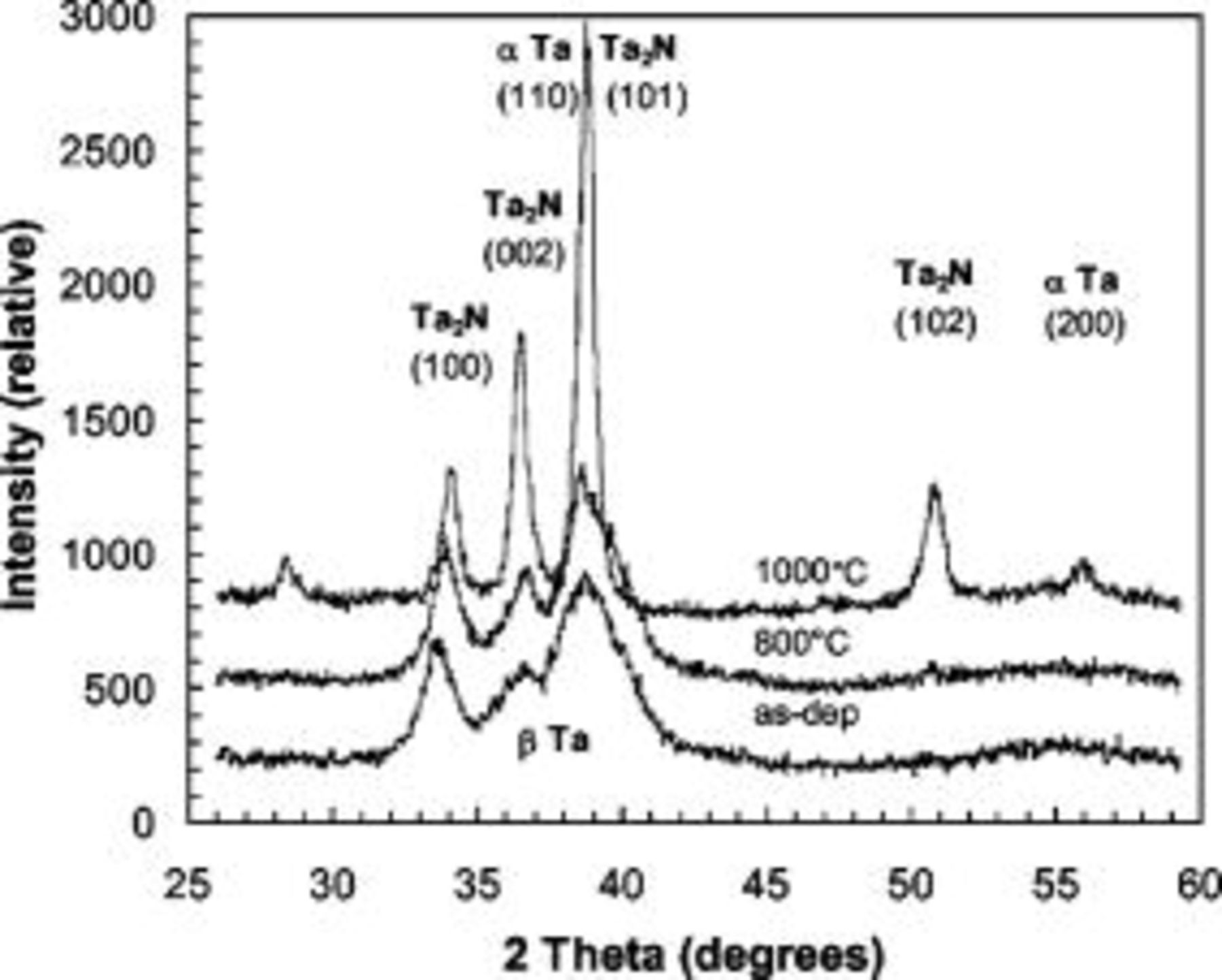
Figure 2. XRD spectra of  Ta electrode as-deposited, and after
  and
and  RTA for
  in
in  . The spectra are offset along the intensity scale to allow data to be distinguished. Note obvious change in film crystallinity (larger grains) and phase (mainly
  , with some bcc-Ta) after the
  RTA.
RTA.
Actual gates have a  cap, but the
  peaks interfere with (and decrease the intensity of) those of the underlying Ta, and so films without
  capping are shown here for clarity. Obtained XRD spectra for gate electrodes with
  capping indicate the same trend, although it is not certain whether as much of the Ta converts to the
  phase with
  capping, as peaks are smaller and more difficult to index. The
  top electrode [bcc α-phase, strongly (110) oriented] peak intensities and positions show no noticeable change after the RTAs, and film remains silvery-metallic in appearance after the RTA.
This reactivity of the Ta with  in the RTA has been confirmed by compositional analysis using MEIS. Using thinner Ta
  electrodes to allow O and N discrimination in the MEIS spectra, a
  Ta film is found to react to a composition of roughly
  after a
  RTA in
  (spectra not shown here). This result is in general agreement with that found by the XRD analysis; namely, that the Ta is very reactive at these high temperatures. There is no direct evidence of tantalum silicide or silicate formation from the MEIS data.
Due to a Ta and La peak overlap in the MEIS spectra, the dielectric film cannot be properly analyzed by MEIS with Ta gate metal present. Therefore, we examined samples without any Ta electrode, to observe the effects of RTA treatment on the lanthanum silicate – silicon interface (understanding that air exposure and trace  in the RTA may affect the dielectric much more being uncapped). Figure 3 compares the MEIS spectra of the as-deposited lanthanum silicate with that after a
  RTA in
  , both uncapped and experiencing a
  in situ reaction anneal. The higher intensity, narrower La peak corresponds to the as-deposited case. It is evident that the
  layer thickens after the RTA. Fitting the MEIS data for the as-deposited film gives a
 film on Si, with no observed interface
  layer.6 The RTA sample fits a graded-layer structure, having a
 surface layer, with a
 oxygen-deficient interface layer. No detectable N was observed in the dielectric by MEIS after the
  RTA in
  . We can conclude that there is a detectable lanthanum silicate–silicon interaction after a high–temperature anneal, resulting in a thicker dielectric layer. However, being exposed to atmosphere might have made the reaction more severe by providing excess oxygen and/or water vapor (which is minimized by quick electrode capping).
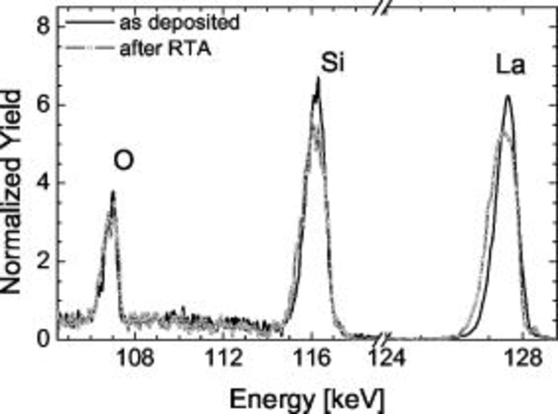
Figure 3. MEIS spectra of uncapped gate stacks, as-deposited (narrow La peak) and after  RTA in
  . Widened La, Si, and O peaks indicate thickening of the lanthanum silicate dielectric (from 1.25 to
  ) after the RTA, revealing some O and La diffusion.
Si and La interdiffusion is one concern when subjecting amorphous  or
or  gate dielectrics to high-temperature processing.7, 25, 26 Recent results from Sivasubramani et al. show that La diffusion into Si from
  is not observed after 1000°C processing, corresponding with a stabilization of the amorphous phase to that temperature,27 consistent with their previous reports on
  .25 As
  has been shown to have a high-temperature stability of the amorphous phase,1 we believe that no significant La diffusion occurs for the devices reported here. Indeed, the integrated intensity of the La peaks in the MEIS spectra (Fig. 3) reveal the same quantity of La in the dielectric before and after the
  ,
,  RTA. As all the C–V curves in Fig. 1 show the same depletion capacitance (same doping level), any La (if present) in the Si would be at concentrations much lower than the doping level of the substrates used. However, a careful analysis using SIMS would be required to confirm the degree of La interdiffusion into Si; this study is in progress.
The film thickness (for the as-deposited case) obtained from the MEIS simulations is thinner than that observed from TEM cross sections and is lower than the expected thickness based on quartz crystal microbalance readings during deposition. TEM cross section of films similarly processed show an amorphous dielectric thickness of at least  ,6 comparing better with our electrical data and expected deposited thicknesses. This discrepancy is not yet resolved but is expected to be due to differences in density between the amorphous dielectric and the bulk values used in the MEIS simulations.
Device Properties with  Gate Electrodes

Using the same process for the lanthanum silicate deposition and reaction annealing,  rf magnetron sputter deposited
  (measured resistivity of
  ) was evaluated for stability with lanthanum silicate in MIS devices. Again starting with low EOT
  devices experiencing only low-temperature processing, the effects of high temperature RTA processing on device C–V characteristics are shown in Fig. 4a, for
  devices measured at
  frequency. Note that the EOT increase with temperature is much less severe than when Ta electrodes are used. After
  for
for  , the EOT is maintained at
  . After
  at
at  , an EOT of
  is obtained, an extremely low value for this processing temperature. As observed with Ta electrodes, a large interface state hump is observed in the C–V curves, which is significantly reduced after the
  RTA (calculated peak
  value
value  ). The effect of frequency on the C–V curve after the
 RTA is shown in Fig. 4b. The presence of interface states is clearly evident from the frequency dependent hump near the threshold voltage, indicative of acceptor states.21
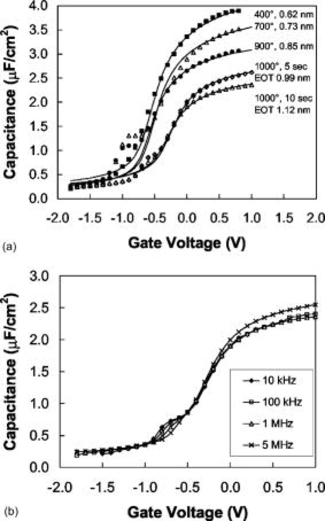
Figure 4. (a) C–V curves from lanthanum silicate MIS devices with 
 electrodes, as a function of RTA temperature (
 device area, measured at
  ). Data is indicated by points, while lines are fits using the CVC program. An EOT less than
  is maintained after a
  ,
,  RTA. (b) C–V curves after a
  RTA at
  , at frequencies from
  to
to  , showing the effects of interface states.
The position of the flatband voltage is slightly lower than for devices with Ta, indicative of a  work function less than
  or an extremely high effective fixed charge density compared to the Ta case. This apparent low work function is in agreement with the
  work function value reported by Pan et al.10 of
  but differs from other reports of 4.5–
 .15, 28 If
  deposition results in higher effective fixed charge (compared to the Ta case), the C–V might be expected to shift more after RTA processing, but it actually shifts less. It is known that high-κ gate dielectrics often give rise to different work functions than for devices with
  dielectric29 and that O vacancies may play a large role,30 but we presently do not know the mechanism responsible for this low apparent work function.
The gate leakage current density of these  electrode devices is shown in Fig. 5 as a function of RTA process temperature. Note that the leakage decreases with increasing EOT caused by the RTA treatment, consistent with the formation of a slightly thicker dielectric. After the
  RTA for
  , the leakage value at
  is about
  .
.
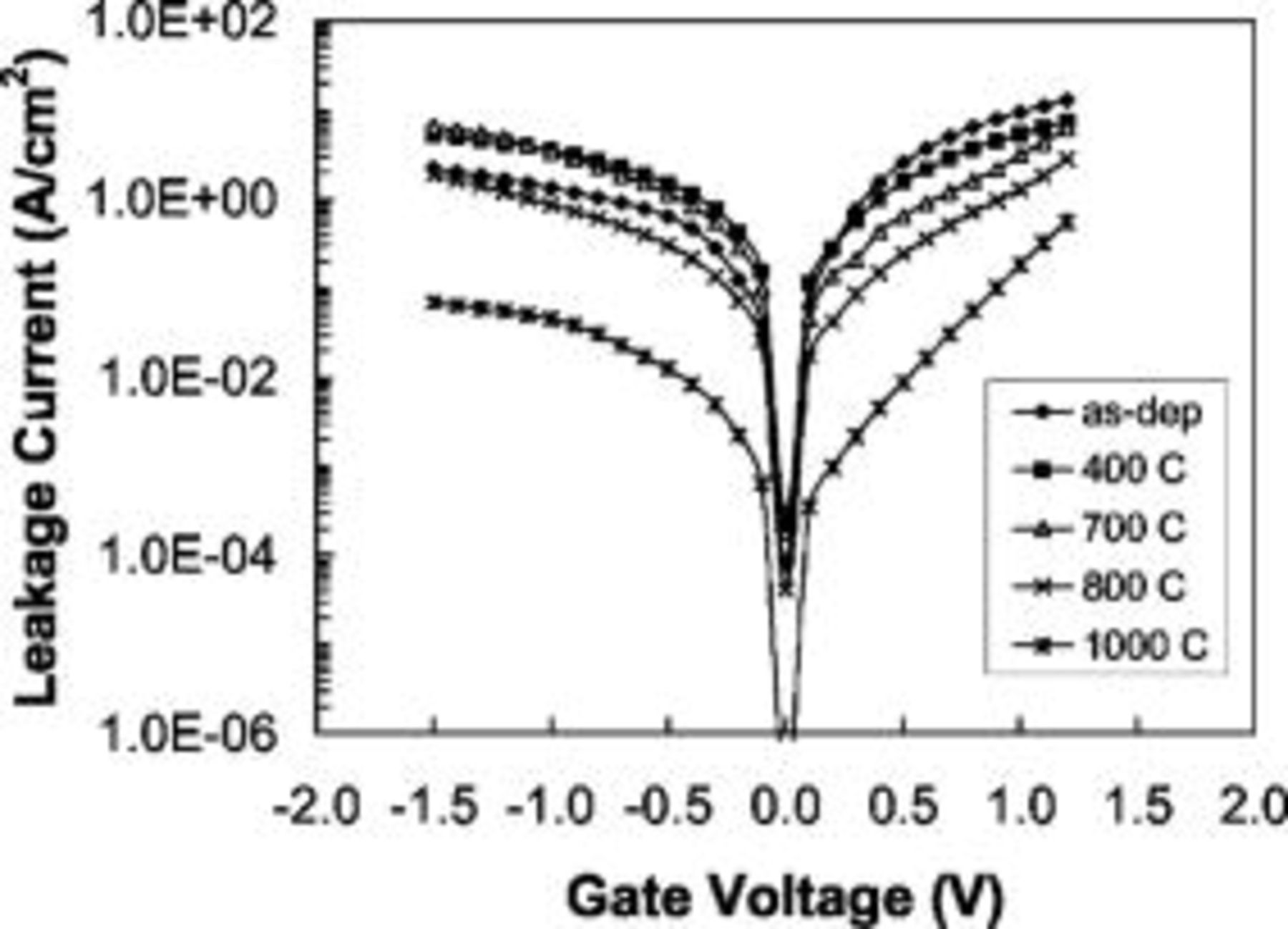
Figure 5. I–V curves for the devices shown in Fig. 4a, with  electrodes, as a function of RTA temperature.
The XRD analysis of these devices (without the  capping for clarity), shown in Fig. 6, reveals a significant difference in the behavior of
  vs Ta electrodes. The diffraction spectra of
  show virtually no change after RTA up to
  , except for a slight change in peak position, consistent with stress relief. This reveals a significant improvement in phase stability over Ta films and corresponds with the electrical properties, showing less change in device properties after annealing. Diffraction patterns of the W-capped gate stack (not shown) after the
  RTA also reveal no obvious change in the
  or the W peaks.
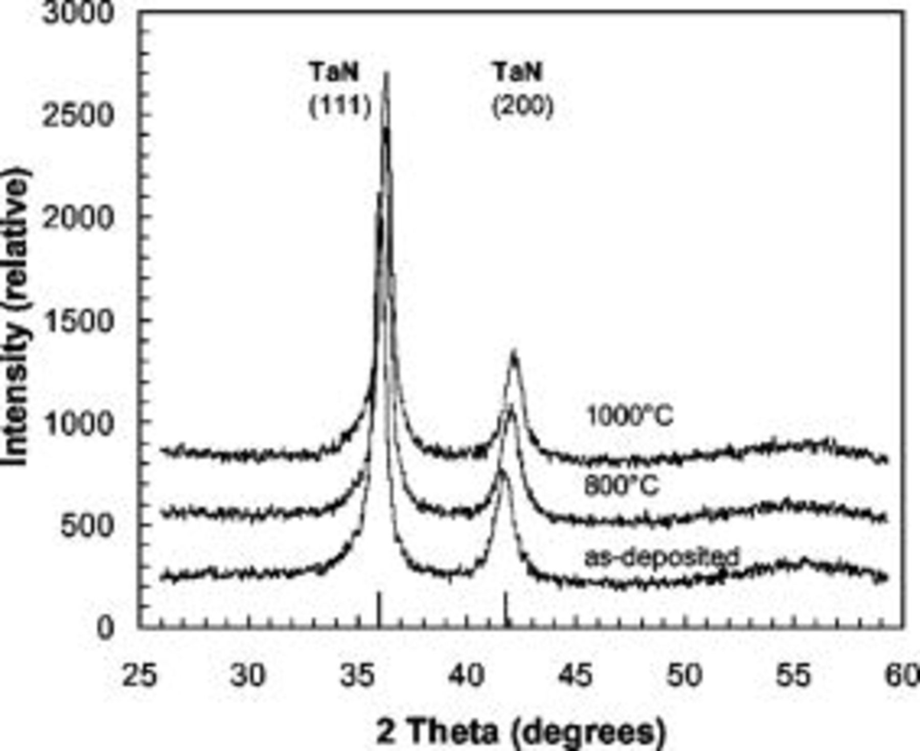
Figure 6. XRD spectra of 
 electrodes. Spectra are offset along the intensity scale to better distinguish data. The only observed change with RTA is a slight shift in peak position.
An overall comparison of device properties can be effectively shown by plotting device EOT vs RTA process temperature and leakage current vs EOT comparing to known  properties.31 Figure 7 shows the EOT as a function of RTA temperature for devices with Ta and
  electrodes (from C–V data shown in Fig. 1 and 4a). Note that for both electrodes the EOT increase is small up to
  processing but the increase in EOT with higher temperature is much faster with Ta gate electrodes. At
  , the gate stack reactions are observed to be very time-dependent, indicated by the different EOT values for RTA times of 5 and
  .
.
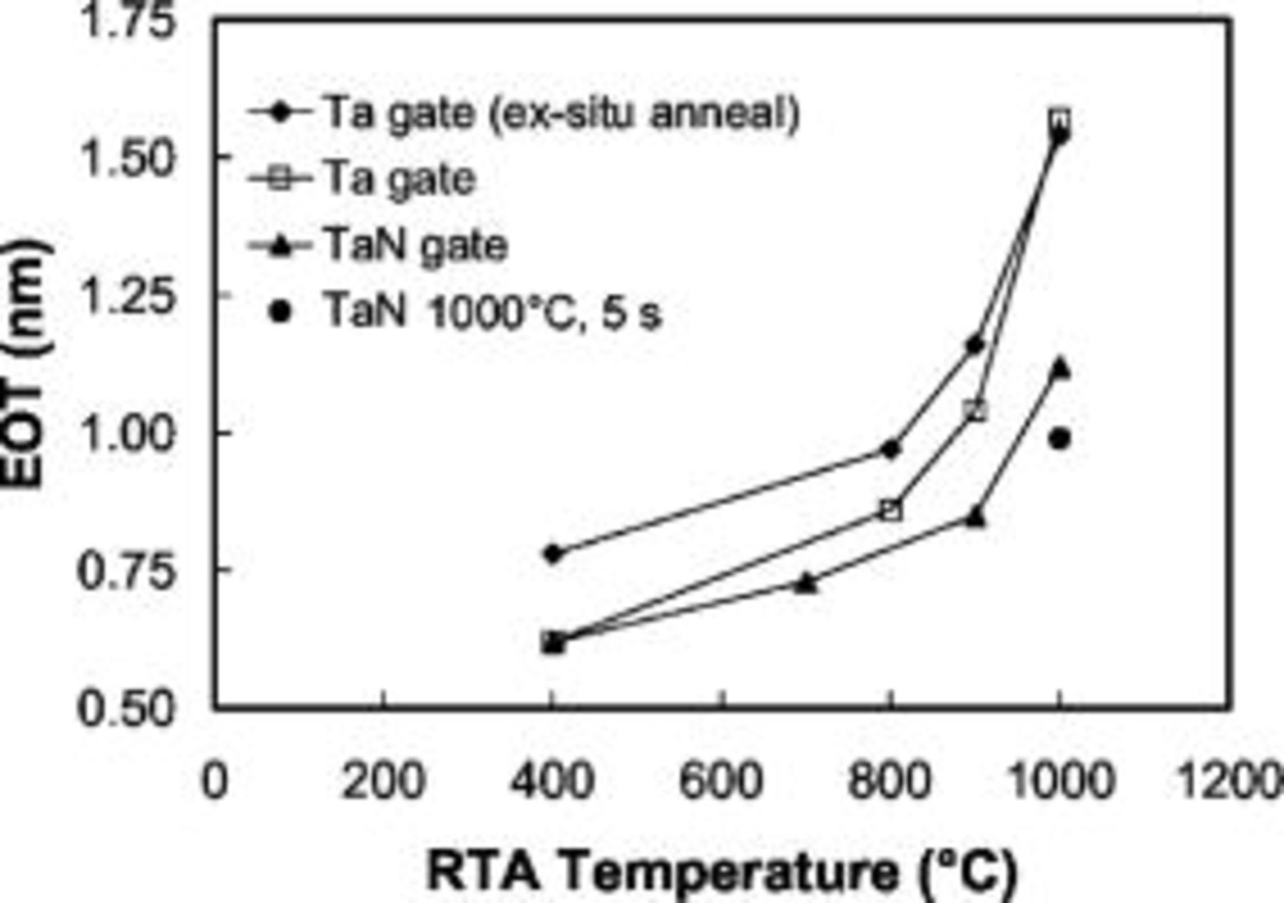
Figure 7. EOT as a function of RTA temperature, for  RTAs in
  . EOT values are obtained from fits to the C–V data of Fig. 1 and 4a. One point is included for a
  electrode stack experiencing an RTA time of
  at
at  .
.
Figure 8 shows the leakage current as a function of EOT for devices with  and Ta electrodes on lanthanum silicate, where the EOT increase has occurred due to high temperature annealing, not due to growing a thicker lanthana film. However, one data point for a thicker lanthanum silicate dielectric having a Ta electrode, experiencing only
  processing, is included for comparison to show how lanthanum silicate leakage scales with EOT in the absence of interface reaction effects. With a Ta electrode, the leakage current is lower than for
  , possibly due to a tantalum oxide (high-κ) or silicate interface formation, or because the E-beam evaporated Ta causes less dielectric damage than the sputtered
  electrode. With increasing EOT (high-temperature processing) note that the Ta data initially closely follows along the
  reference slope. However, above
  processing the leakage does not decrease as expected, further indication of reaction effects between the lanthanum silicate and the Ta gate electrode. With
  , the leakage data follows the expected slope, indicative of little interface reaction between the electrode and dielectric.
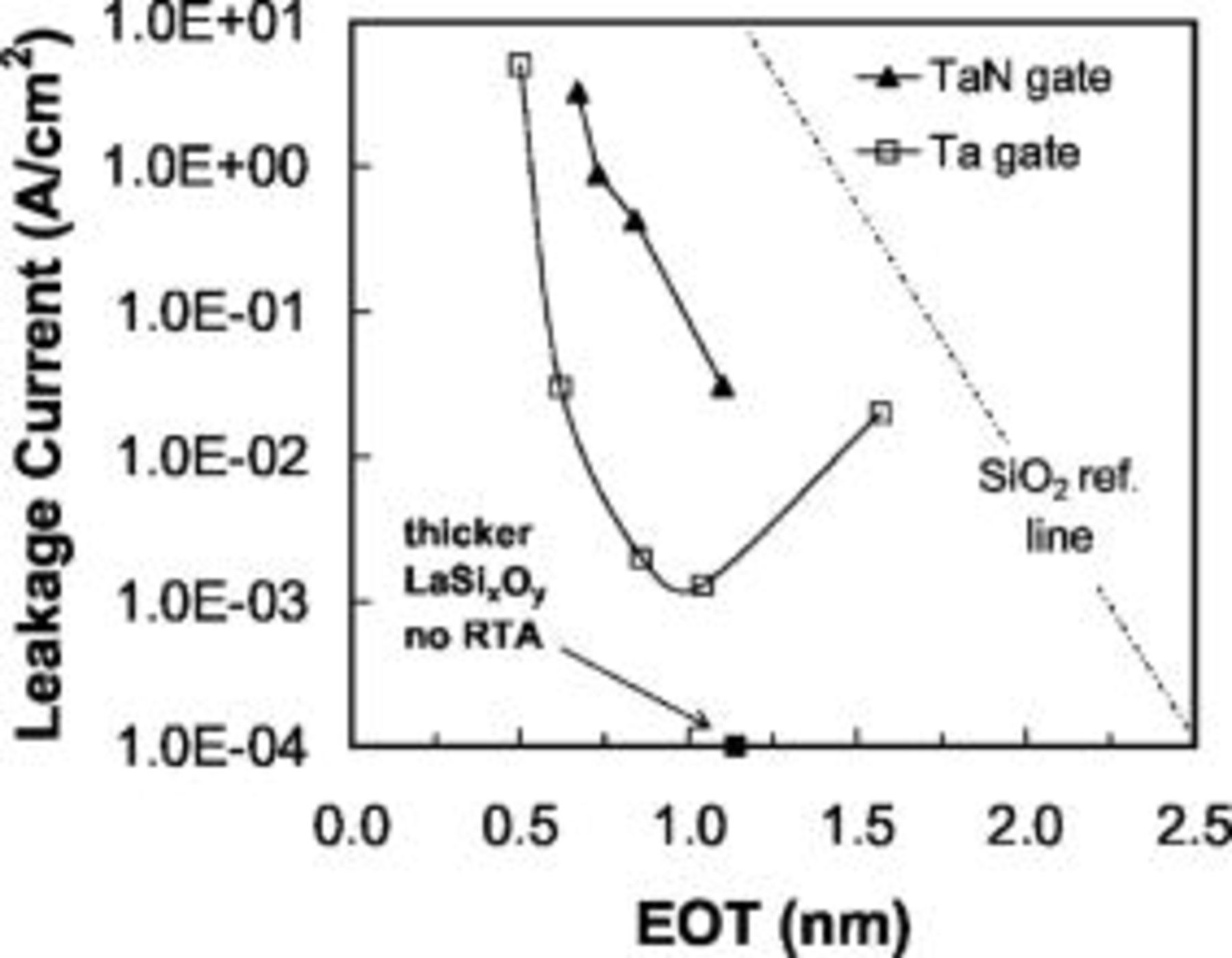
Figure 8. Plot of leakage  for devices with
  and Ta electrodes, after high-temperature processing. Included is a reference line for
  at
at  from Lo et al.31 Data from a thicker lanthanum silicate MIS device with a Ta cap, experiencing only
  processing, is included (EOT
  ,
,  ) to demonstrate that leakage decreases as lanthanum silicate thickness increases, in the absence of interface reactions.
As the EOT does increase with  electrodes, apparently some additional oxygen or nitrogen incorporation causes dielectric growth (although much less than observed with Ta electrodes). Other studies have shown the difficulties of removing all unwanted O from the gate electrode;32 presumably one key reason that
  is an improvement over Ta (related to its better stability) is the decrease in O diffusion through it. Further study is required to fully determine the origin of the leakage difference between using Ta and
  electrodes and to determine whether or not N from the
  incorporates in the lanthanum silicate dielectric layer, which can affect the bandgap33 and other properties.
Conclusions
Gate stacks with a lanthanum silicate dielectric and either Ta or  electrodes have been produced with EOT values of
  , with leakage at
  less than
  with a Ta electrode. However, if the gate stack is subjected to high-temperature processing, EOT values increase and the gate electrode material choice becomes of key importance. We have observed by both XRD and MEIS that Ta undergoes a phase transformation and grain growth after a
  ,
,  RTA in
  ambient. This corresponds with a device EOT increase to
  or higher. Alternatively, utilizing
  as the gate electrode, XRD shows virtually no change in the electrode material for RTA temperatures up to
  . The corresponding device characteristics show less degradation, with EOT remaining as low as
  after
after  at
at  , or
, or  after
after  with corresponding leakage of
  . From these results, combined with MEIS spectra from uncapped dielectric on Si, device degradation seems to arise mainly from interactions with the Ta electrode, and partly from Si–dielectric interaction. Further steps are required to eliminate interface reactions, although these EOT and leakage values are very promising from a device application standpoint. Interface defect densities remain at rather high levels even after the high-temperature RTA, and minimizing these remains a challenge for this and other high-κ dielectrics on Si.
Acknowledgments
The authors thank L.V. Goncharova, T. Gustafsson, and E. Garfunkel at Rutgers University for MEIS analysis, and the Semiconductor Research Corporation for project support.
North Carolina State University assisted in meeting the publication costs of this article.
Footnotes
- d
For devices with high densities of interface states, modeling the C-V curve accurately in the depletion region is difficult. An uncertainty thus exists in the calculated doping level, and flatband voltage. However, the calculated EOT value is not affected.