
Abstract
A copper hillock induced interconnect failure mechanism is presented. The copper hillock is frequently generated during a copper dual damascene process and hillock formation is found to degrade the interconnect integrity by affecting the following process steps. The copper hillock appears to damage the  capping layer and results in copper corrosion during via etch. The corrosion generates copper particles inside via holes and the defects are found to make the following metal depositions incomplete during via formation. Based on the observations, a copper hillock induced defect model is proposed and a new copper process is suggested to reduce copper hillocks.
Export citation and abstract BibTeX RIS
The copper dual damascene process has been widely employed for fabricating multilevel interconnection schemes in advanced very large scale integration (VLSI) technology due to its low bulk resistivity and good electromigration (EM) resistance.1 However, when adopting copper as a interconnect metal, many issues arise. For example, a diffusion barrier is required for copper diffusion inhibition in the metallization because of the high diffusivity of copper through oxide and silicon.2, 3 Also, copper has a high thermal expansion coefficient compared to other materials used in VLSI technology and such a characteristic results in thermal stress in a stack of copper and dielectric layers. The thermal expansion mismatch of copper and interlayer dielectric (ILD) layers was reported to cause hillock defects.4
When a copper layer underneath silicon oxide or silicon nitride is heated during the manufacturing process, it undergoes a compressive stress, which can be relieved by forming a copper hillock.5, 6 Other research has reported that plasma cleaning plays a dominant role in hillock formation.2 Also, grain boundary migration was found to be critically involved in the electromigration induced hillocks.7
Although there has been much research on the root cause of copper hillocks, there has been little research on how the hillock leads to interconnect failure. Some authors have reported that a hillock-induced failure mode in aluminum metallization is described as an interlevel metal short caused by theta phase hillock.8 But considering the typical size (sub- ) of the copper hillock formed in a copper metallization, it is unlikely to have a copper hillock induced intermetal short. To date, a direct correlation of copper hillock to interconnect failure has not been reported. In this paper, we investigate an interconnect failure mechanism caused by the copper hillock and propose a model for copper hillock induced defects.
Experimental
An  ., (100)-oriented, p-type silicon wafer was used as a starting material. Dual damascene structures of
  were fabricated to evaluate the effects of hillock during the manufacturing process (Fig. 1).
  and copper were deposited on the
  by the physical vapor deposition and electrochemical plating and then the test wafers were planarized by copper chemical mechanical planarization (CMP). The surface of these sample was treated with
  plasma at the substrate temperature of
  .
.  films
films  thick were deposited on the sample by plasma chemical vapor deposition using
  and silane gases. The plasma power, gas pressure, and substrate temperature in the deposition process were
  ,
,  , and
, and  , respectively. After completing the process, many copper hillocks were observed on the copper surface. Using these samples, via first dual damascene was processed to reveal the effect of copper hillock. First, ILD material was deposited by plasma chemical vapor deposition at
  and a via hole was patterned and etched.
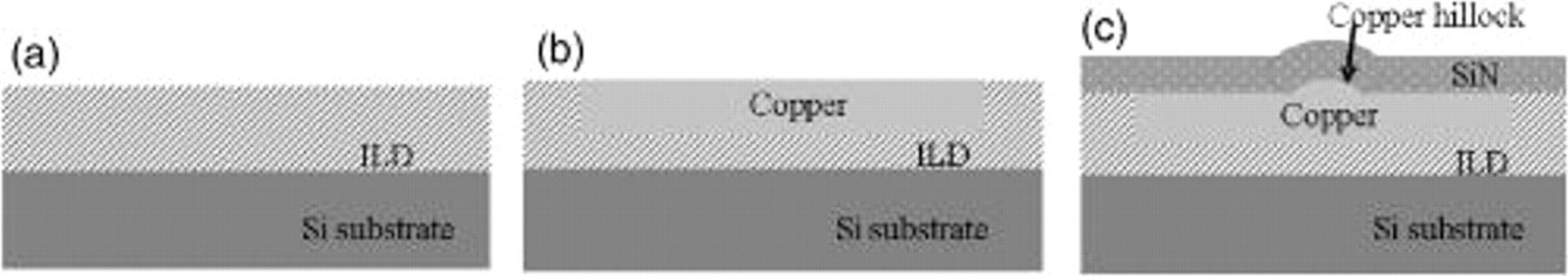
Figure 1. Sequences of wafer preparation. (a) ILD was deposited on the silicon wafer. (b) A copper interconnect was formed using dual damascene process. (c) Copper hillock was induced by thermal stress during  deposition process.
In each process, step by step inspection including defect scanning and review was performed. After the trench ash process was completed, unknown particles were found on the via hole, which was formed upon the copper hillock at the sublayer level. The particle was analyzed by Auger electron spectroscopy (AES), scanning electron microscopy (SEM), and atomic force microscopy (AFM).
Results and Discussion
Figure 2 shows the results of step by step inspection. First, we have identified a copper hillock after ILD deposition. After the via ash, an abnormal hole pattern was formed at the identical location and then an unknown defect was observed after trench ash (Fig. 2c). To confirm the chemical composition of the defect, AES measurement was performed near the defect. Figure 3 shows qualitative analysis by AES for the defect region and a defect-free region. AES results reveal that a much higher copper content was detected in the defect region compared to the defect-free region. Based on these results, we believe the defect must be related to underlying copper, ruling out the possibility of a typical polymeric byproduct (Fig. 3). Figure 4 shows a cross-sectional image of the region where the defect lies. Copper void and copper corrosion were observed under the defect. Partial  lift-off in the via hole was observed only where the copper hillock was located, while other via holes had undamaged
  layers. The image implies that the
  barrier layer over the copper hillock may be damaged during the via etch even though the etch should have an excellent selectivity over the
  layer. Copper diffusion or corrosion may be enhanced through the damaged
  layer. A similar observation was been reported in Ref. 9, showing that pits occurred on the surface of the
  barrier when it was annealed at
  or higher and then enhanced copper diffusion into
  layer, resulting in a copper void.
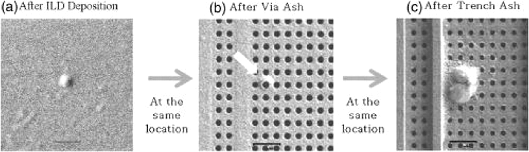
Figure 2. Top view SEM micrograph of the defect at each step. (a) Copper hillock was observed after ILD deposition. (b) Abnormal via hole existed at the same location after via ash. (c) Unknown defect was also observed at the same location after trench ash.
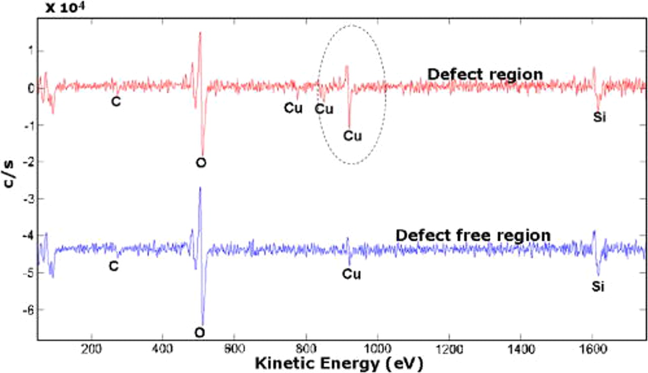
Figure 3. (Color online) AES component qualitative analysis for the defect after  ion sputtering.
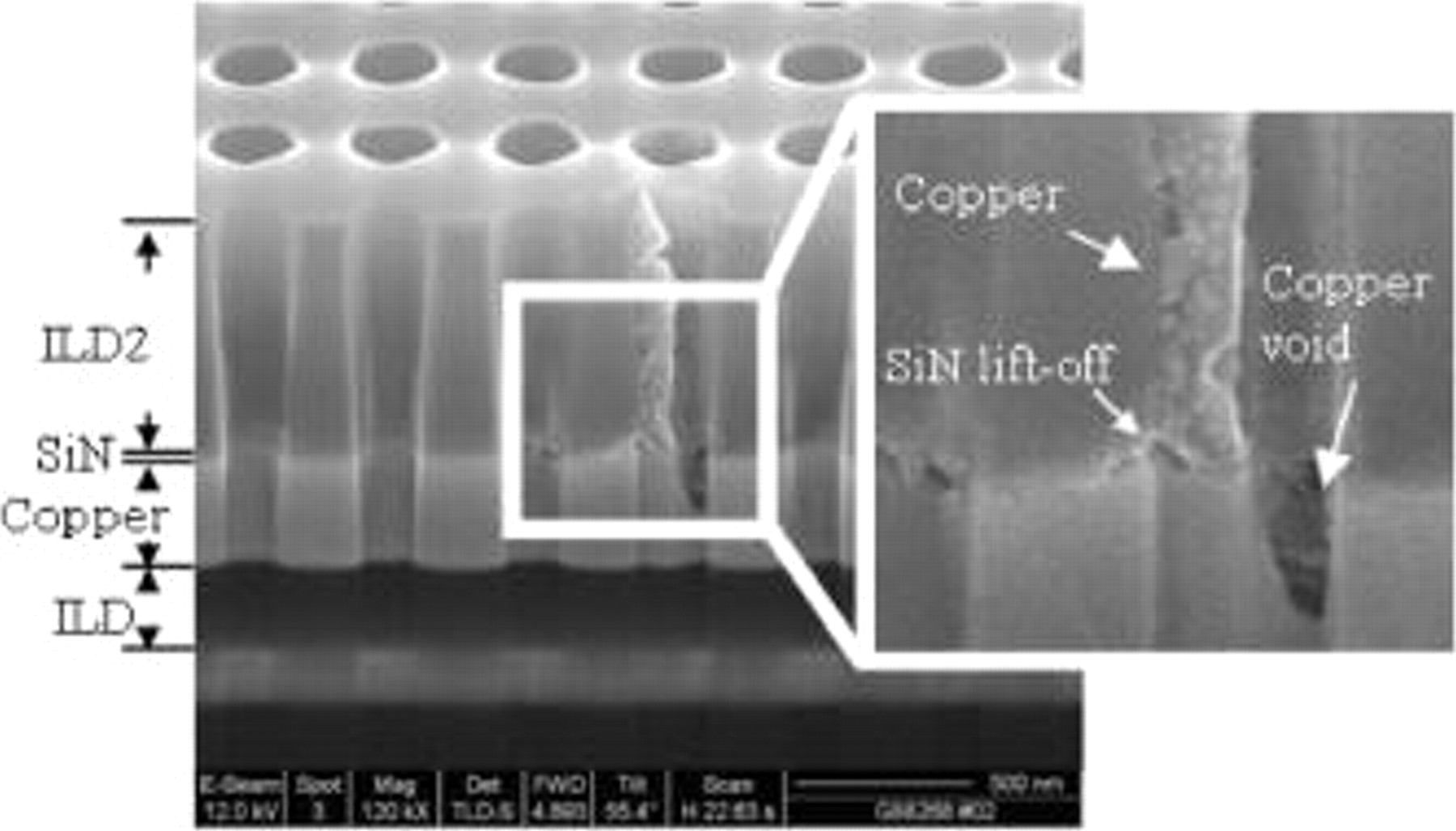
Figure 4. Cross-sectional view of SEM micrographs under the defect.
Based on the analysis, we propose a model for copper hillock induced interconnect failure as illustrated in Fig. 5. First, a copper hillock is formed under compressive stress during  deposition process. In comparison, the
  layer around the hillock undergoes tensile stress, which weakens the
  layer because
  is normally brittle. When a via hole is formed on the hillock, the stressed
  is easily susceptible to plasma-induced damage and becomes weaker. Copper underneath the damaged
  layer is able to diffuse through the
  layer, and when exposed to gas ambient during the subsequent etch and ashing processes, copper agglomeration is protruded by the copper corrosion. The generated defect renders the following metal deposition incomplete by blocking the deposition and results in via voids.
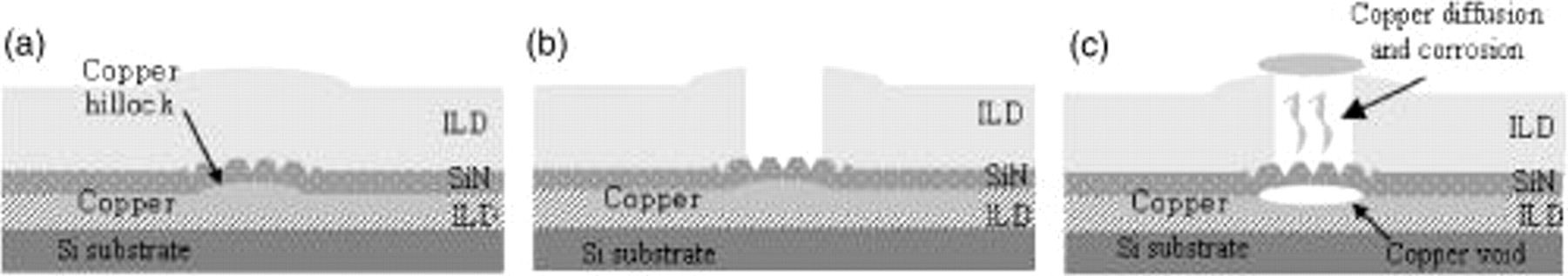
Figure 5. A model for copper hillock effect. (a) Cu hillock makes  lift-off and break. (b) Oxide etch is processed on it. (c) Copper corrosion occurs during subsequent process through copper diffusion and results in copper voids.
Therefore, to prevent defect generation, it is important to suppress copper hillock formation. In this paper, a fabrication method of suppressing the copper hillock formation is suggested. The proposed process involves a preanneal process at  for
for  and touch up copper CMP for
  between copper CMP and ILD deposition process. Figure 6 illustrates a new process flow compared to the conventional process. Figure 6 also shows AFM images of the wafer surfaces obtained using the conventional process and the proposed process. According to the AFM images, the number and size of the copper hillocks appeared to be significantly reduced using the proposed process. To quantify the improvement, the surface roughness was measured using AFM over
  as shown in Table I. The average and variation of the surface roughness greatly improved using the proposed process. The surface roughness measurement confirmed less copper hillock can be formed by performing additional anneal and CMP. We believe that the improvement may be attributed to the released thermal stress by additional CMP process.
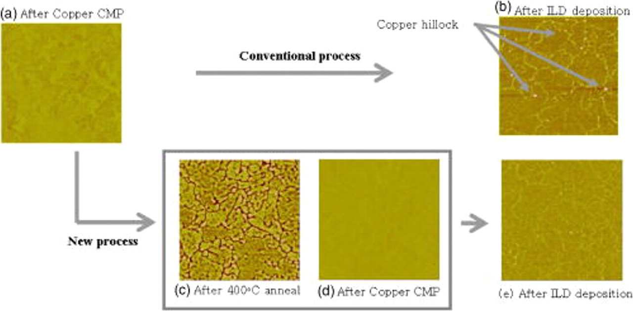
Figure 6. (Color online) AFM image comparison between conventional process and new process. A few hillocks are observed after ILD deposition in the conventional process (a and b). Additional furnace anneal and copper CMP processes were performed in the new process and a significant reduction of the hillocks was observed (c–e).
Table I. Surface roughness measurements using AFM for the conventional and new processes.
| Conventional process (nm) | New process (nm) | |
|---|---|---|
| Rmax |

|

|
| Ra |

|

|
| RMS |

|

|
Conclusion
For the dual damascene process, the effect of copper hillock on metal interconnect integrity was investigated. The copper hillock was found to degrade the copper diffusion suppression ability of  layer, resulting in copper voids and copper corrosion. Based on the observations, we conclude that the copper hillock can be one of the root causes for incomplete via formation, leading to an open via problem. To minimize the number of copper hillocks, a new fabrication method is suggested. By performing an additional anneal process and a copper CMP process prior to IMD deposition, the number of copper hillocks was dramatically decreased. We believe that the suppression of the copper hillock formation may be attributed to a relieving of thermal stress in the copper.
Acknowledgments
The authors thank many personnel at Dongbu Electronics Inc. for their assistances and encouragements during this work. This work is supported by the national project of COSAR (System IC 2010) and TND.
Dongbu Electronics assisted in meeting the publication costs of this article.