
Abstract
Large-scale nickel nanocones array are synthesized by a one-step electrodeposition method without any template. The size and apex angle of nanocone can be controlled by changing the current density and deposition time. The mechanism of the formation of nanocones array morphology has been discussed. This nanocones array shows very good field emission properties with low turn-on field of  (corresponding to an emission current of
  ) and large currents of
  . The shape and density of the nanocones significantly affect the field emission properties.
Export citation and abstract BibTeX RIS
Nanostructures with high aspect ratios, such as nanowires, nanorods, and nanotubes, have attracted much attentions due to their potential applications, such as interconnects in nanofabrication,1 optoelectronics,2 nanosensors,3 and nanobiotechnology.4 It was reported that the properties of the nanostructures were affected by their size and morphology,5–7 which subsequently prompted extensive efforts to control them. The synthesis of metal nanostructures, such as nanobelts, nanorods, and nanowires of nickel, copper, silver, and gold, has been demonstrated using various methods.8–15 However, the randomness inherent to most of these synthesis method has largely prevented the resulting nanostructures from being integrated into high density electronic and optoelectronic devices. Among all these nanostructures, ordered nanocones array has stimulated an increasing research interest as the nanocones have some potential applications for scanning probe and field emitters with superior properties to nanotubes.16–18 In the last  , only a few examples of the fabrication of metallic nanocones have been reported and the synthesis methods were mainly template-based.19–22 Although these nanostructures are highly ordered, the nanostructures (e.g., length and radius of nanocones) of materials prepared by means of the template-based synthesis are limited due to the available dimensions of the templates. The densities as well as the diameters of the metallic nanocones fabricated by these methods are restricted to the pore diameter and separation wall thickness of the template. Moreover, the preparation processes and steps of template-based methods are much more complicated than a simple one-step process without the employment of templates.23, 24
In this paper, we present a detailed structural analysis, based on a scanning electron microscope (SEM) and transmission electron microscopy (TEM) study, of nickel nanocones array grown by this one-step electrodeposition method that is suitable for integration into field emission devices. The analysis elucidates the growth mechanism of the nickel nanocones array, specific to the special modifying agent used, which does not require templates or catalysts. The relationship between the morphologies of nanocones and the field emission characteristics was investigated which indicates that the Ni nanocones array is a promising electron emitter. Furthermore, in our latest research, the synthesis procedure for the Ni conical nanostructure has been confirmed to be appropriate for the fabrication of Co nanocone arrays and considered adaptable to some other metals. Since this one-step method without any templates is rather simple and economical, the synthesis process is also expected to be appropriate for commercial application.
Experimental Procedures
The field emission nanocones arrays (FEAs) Ni films were grown on the substrates of copper predeposited glass by a method previously described that uses ethylenediamine dihydrochloride as a crystal modifier.25
Substrate and electrodeposition solution
The substrates of Ni FEAs were copper predeposited glass. Glass slides  were cleaned by ultrasonic methods. First,
  Cr and then
  Cu were deposited on slides by magnetron sputtering at room temperature. The electrodeposition solution was composed of analytical pure
  (providing Ni ions),
  (
( buffer), and crystallization conditioning agent with concentration of 200, 35, and
  , respectively, dissolved in deionized water.
Fabrication of Ni Nanocones Arrays
A pure Ni plate (99.9%) is used as an anode, while as sputtered slides are used as cathode for Ni FEAs deposition. The temperature of deposition solution was kept at  and
and  value was 4.0. The deposition current density was
  . The deposition time was 112, 450, and
  , respectively, to obtain Ni nanocone FEAs with different morphologies.
Characterization
The morphology and structures of Ni nanocones arrays were analyzed by scanning electronic microscopy (SEM), (USA, FEI Sirion 200), transmission electron microscopy (Japan, JEM-2010, JEM 2100F), and high-resolution TEM (HRTEM; Japan, JEM-40001X). X-ray diffraction (XRD) was conducted on a Bruker D8 Discover X-ray diffractometer equipped with Cr radiation  .
.
Field emission measurement
The samples were cut into  pieces for field emission measurements. Experiments were carried out in a field emission measurement system at pressure of about
  with a tip-to-anode distance of about
  . A voltage was applied between Ni nanocones and anode plate. While increasing the voltage step by step, the applied voltage was recorded and the emission current was measured by an electrometer with a current sensitivity of
  .
.
Result and Discussion
The SEM images of three Ni nanocones arrays deposited at the current density of  for 120, 450, and
  are shown in Fig. 1a, 1b, 1c, 1d, 1e and 1f. It can be seen from the figures that most of the nanocones grew in the same direction vertical to the substrates. The average root diameters of the nanocones were estimated to be about 160, 380, and
  and the heights were 300, 750, and
  , respectively. The densities of cones on the field emission arrays were estimated to be about
  ,
,  , and
, and  , corresponding to the extending deposition time, which are very high in comparison to the density of other field emission array reported before.4 However, the apex angles of all these cones are almost the same as 35°. It is indicating that the size of the nanocones can be controlled by the electrodeposition time, while the shape of the cones did not change with the time. Figures 1d, 1e and 1f show the high-magnification SEM images of a single nanocone deposited at
  for
for  from different angles of view. It is clear from the figures that the vertical nanocone was growing up spirally with obvious steps. The top view image also indicated that the nanocone has five side planes forming a pentagonal pyramid tip.
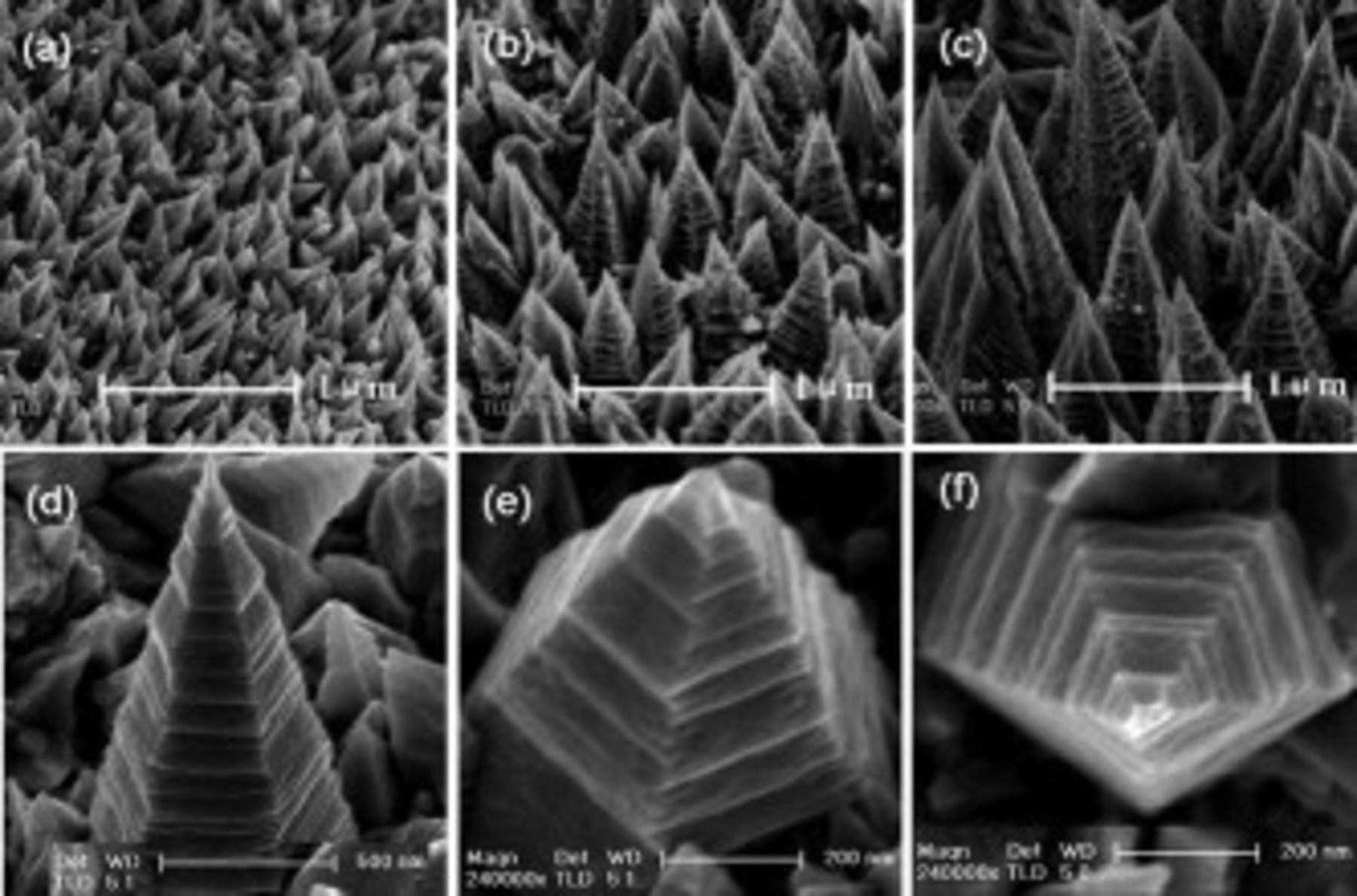
Figure 1. The SEM images of Ni nanocones array deposited for (a)  , (b)
, (b)  , (c)
, (c)  ., and high magnification images of a single nanocone from different angle of view (d) side view, (e) 45° to the substrate, (f) top view.
The morphology and structure of a single nanocone were analyzed by TEM. Figures 2a and 2b show the morphologies of two nanocones deposited at the current density of 2 and  . The apical angles of the cones measured from Fig. 2a and 2b are about 35° and 20°, respectively, which indicate that the sharpness of the nanocone is greatly increased with higher deposition current density.
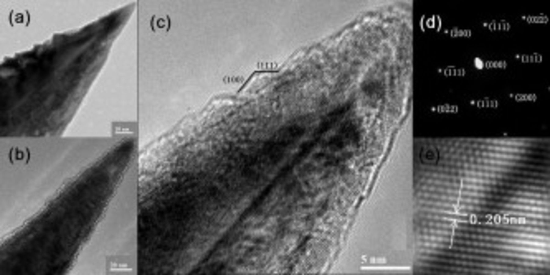
Figure 2. [(a), (b)] Bright TEM images of Ni nanocones deposited at the current density of  and
and  . (c) High-resolution transmission electron microscopy (HRTEM) image of a single Ni nanocone. (d) Microdiffraction pattern for that single nanocone. (e) Enlarged view of the HRTEM image of that nanocone shown in (c).
The structural orientation of an individual nanocone was investigated by high-resolution TEM, as shown in Fig. 2c; an enlarged view of the same image is shown in Fig. 2d. The image of the {111} nickel lattice planes with a space of  between the neighboring lattice planes, in agreement with
  space of face-centered cubic-nickel (fcc-Ni), with no disruption of the lattice planes, indicates that the nanocone is a perfect single crystal; this was true in the majority of nanocones observed. Figure 2e shows a typical selected-area electron diffraction (SAED) pattern that was recorded from this nanocone; it can be indexed to be the [011] zone axis of the fcc-Ni. These pattern spots also demonstrate the single crystallinity of this nanocone. Both the HRTEM image and SAED pattern demonstrate that growth direction is close to [011]. This result is confirmed by XRD analysis shown in Fig. 3. The three diffraction peaks in good concordance with JCPDS card (04-0850) can be indexed as face-centered cubic (fcc) Ni with lattice constant
  . The texture coefficient of each crystal face can be calculated by the formula:
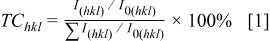
where  and
and  indicate the diffraction intensities of the Ni deposits and the standard Ni powder, respectively. The results are
  , while
  and
and  , which indicates that the Ni electrodeposits' preferred orientation is (110). This direction is the same to the zone axis of fcc Cu nanowires that had previously been reported by Kim.26
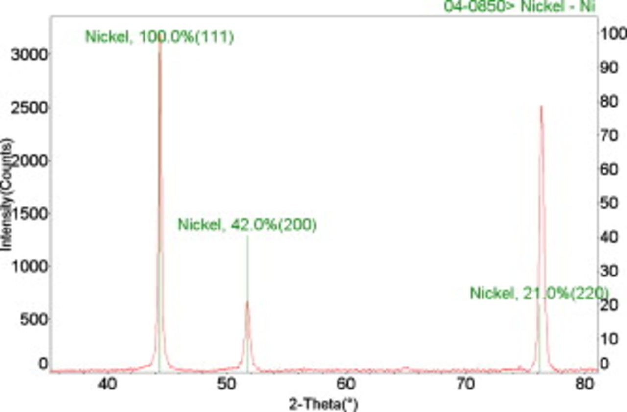
Figure 3. XRD pattern of the Ni nanocones array deposited on the Cu predeposited glass at the current density of  for
for  .
.
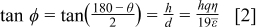
The growth mechanism of the nanocones by this electrodeposition method can be explained by the screw dislocation growth on a real crystal surface with defects.27 Due to the helicoidal structure of this crystal imperfection, a step originates from the point where the screw dislocation line intersects the surface of the crystal face. This step is constrained to terminate at the dislocation emergence point and winds up into a spiral during the growth process. The schematic of the screw dislocation growth is shown in Fig. 4a and 4b. By the theory further developed by different authors,28–36 it is not so difficult to explain the relationship between the apex angle θ of the nanocone and the current density (corresponding to overpotential η). As shown in Fig. 4c, the slope of the nanocone  can be predicted by the equation:
where  is the current quantity at each turn of one monolayer and ε¯ is the boundary energy.
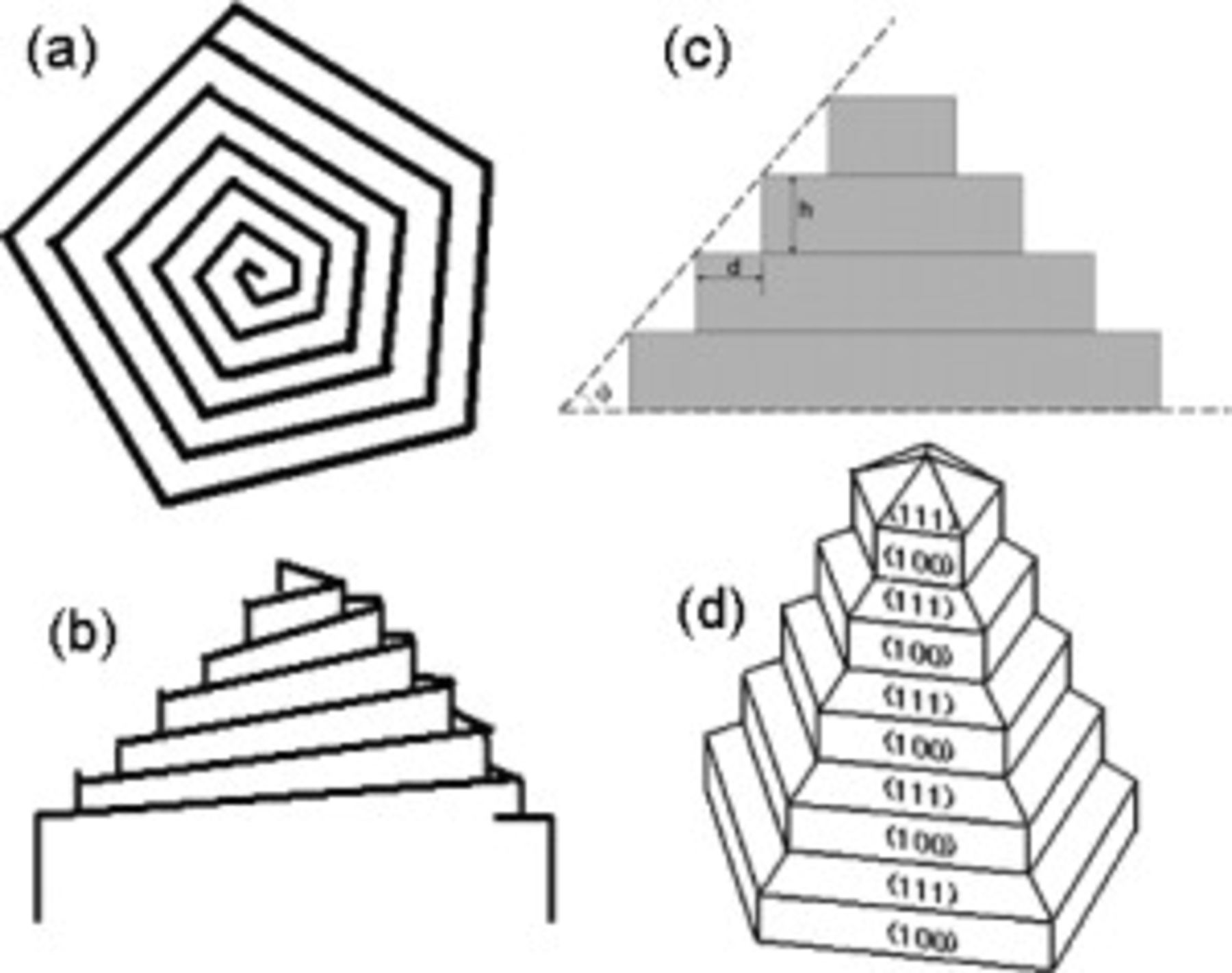
Figure 4. The schematic illustration of the nanocones growth mechanism. (a) side view, (b) top view, (c) the relationship between the apex angle of nanocone and the current density, and (d) the crystal morphology with different crystal surface.
Grown under these conditions such crystal faces can exhibit a few single screw dislocations only which produce growth cones with a uniform slope (Fig. 4c). In a later stage of growth the pyramids cover the whole crystal face, forming a nanocones array surface structure with a uniform step density.
The [110] growth direction of the nanocones is due to the different velocity of growth on different crystal surface. According to previous report,37 the sequence of the exchange current densities  (corresponding to the growth velocity) on different crystal surfaces of fcc nickel are
  . Figure 4d shows the relation between the crystal surface and the crystal morphology. The faster growing surfaces (110) tend to disappear, while the slowly growing surfaces (111) become the final surface of the crystal. This explains why the nanocones were growing along the [110] direction. The fivefold structure of the Ni nanocone is similar to the structure of Cu nanowire which has been well elucidated by Kim.26 It is believed that fcc metal nanocones are also grown from multiple twinned decahedral seeds confined by the twin planes and side planes.38–40 Confinement of the (111) side planes was implemented successfully to grow metal nanocones in solution using ethylenediamine dihydrochloride as capping agents.
Owing to their sharp tips and controlled growth, the present Ni nanocones arrays fabricated by electrodeposition may prove to be useful as electron emitters and in fabricating electronic nanodevices. To assess this, the current–voltage  characteristics of the Ni nanocones arrays were measured using a field emission measurement system at pressure of about
  with a tip-to-anode distance of about
  . While increasing the voltage applied between Ni nanocones and anode plate step by step, the emission current was measured by an electrometer with a current sensitivity of
  .
.
The results of  measurements of Ni emitters are shown in Fig. 5a. It can be seen from Fig. 5a that the turn-on fields of Ni nanocones arrays are 5, 6.1, and
  corresponding to deposition time of 120, 450, and
  , respectively. The morphologies are shown in Fig. 1a, 1b and 1c. All turn-on fields are relatively lower than previous reports, corresponding to a significant large emission current of
  which is 10–1000 times more than the commonly reported value
  in earlier research papers.44, 45 To all the Ni nanocones arrays, at an applied electric field of
  , obvious field emission currents have been observed and are 141, 49, and
  , respectively, for 120, 450, and
  deposited Ni nanocones. When applied electric field increases to
  , field emission currents of all nanocones arrays are up to
  . All of the three Ni nanocones arrays have pretty good field emission properties. Compared with the other two samples, nanocones arrays grown for
  have the best performance: at an applied electric field of
  , there is a tremendous field emission current of
  .
.
Figure 5. Field emission properties of Ni field emission nanocones arrays. (a) Measured emission current vs applied voltage; (b) F-N plots and the linear fit slopes.
In general, Fowler–Nordheim (F–N) theory is used to describe field emission characteristics of metals,41 which is expressed as:
where  is the emission current density that is expressed as
  , where
  is the total emission current in the unit of microampere and
  is the effective area of electron emission (centimeter square),
  is the applied macroscopic field that is expressed as
  , where
  is the applied voltage in volts and
  is the distance between the plane anode and cathode
  , φ is the work function of the emitter, which is
  for nickel,
  and
and  are the constants with values of
  and
and  , respectively, and the FE enhancement factor β is introduced to quantify the degree of enhancement of any tip over a flat surface. It represents the true value of the electric field at the tip compared to its average macroscopic value. For metal, with typical work function and a flat surface, the turn-on field is typically around
  , which is impractically high.42 On the other hand, sharp tips could induce field enhancement and the effect is described in terms of field enhancement factor β. As a result, all the field emission sources tend to have smaller sizes because of the primary role of the β factor: the larger the β, the higher the field convergence and enhancement, and therefore the lower the practical turn-on voltage for emission.43 Equation 3 can be further derived as
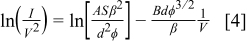
Therefore, the slope can be obtained from the F–N plot,  versus
  , as
, as  . The F–N plots as well as the linear fit slopes are presented in Fig. 5b. With the increase of deposition time from
  , the curves shifted from lower voltage region to higher one, i.e., the emission currents decreased at the same electrical field as deposition time increased. With the deposition time prolonging, the performance of nanocones array is worsen because of Ni nanocones unsharpening, coarsening, and disordering, as shown in SEM images (Fig. 1a, 1b and 1c). According to F–N plots (Fig. 5b) and F–N equation, the estimated field enhancement factor β decreases from
  to
to  , indicating the decrease of nanocones sharpness. The field emission properties corresponding to the shape and size of Ni nanocones could be varied by changing the deposition time and current density. With deposition time extending, Ni nanocones will be getting less sharp and burrs will increase, resulting in deterioration on field emission performance, which shows a deeply dependent on cones morphologies (especially sharpness). Through further study on controlling the morphologies of nanocones array by other deposition conditions, optimized parameters would be obtained to fabricate Ni nanocones arrays with better field emission performance.
Conclusion
In summary, a simple method of Ni nanocones arrays fabrication by electrodeposition was studied in this work. SEM observation indicates that the size and shape of the Ni nanocones can be controlled, and the TEM study proves that the vertical nanocone was growing up spirally along [110] direction. Test by vacuum field emission measurement system shows that the nanocones array field emitters have low turn-on fields for  , corresponding to a large emission current for
  . Large emission currents of
  were also obtained.
This method provides a simple and low-cost approach to fabricate field emitters. It would probably provide an economic way to meet the industrial requirements of low-cost processing techniques for the large-scale production of nanomaterials with acceptable FE performance and engineered surface functionality.
Acknowledgments
This work was sponsored by the National Natural Science Foundation of China (Grant no. 90406013), Shanghai Pujiang Program (Grant no. 05PJ14065), and Shanghai Nanotechnology Promotion Center (Grant no. 0452nm030). We thank Dr. Hu in Jilin University for the help on field emission measurement and the Analytical and Testing Center of Shanghai Jiao Tong University for the help on SEM observation.
Shanghai Jiao Tong University assisted in meeting the publication costs of this article.