
Abstract
Scintillators, which convert high-energy rays such as X-rays and positrons into visible and ultraviolet light, are incorporated as radiation detectors in X-ray computer tomography (X-ray CT) and positron emission tomography (PET), which system performances highly depends on the characteristics of the scintillator used. In this study, SrGa2S4:Eu/ZnO vertical nanowires (ZnO-vnws) bilayer scintillators were fabricated by electrodeposition of ZnO-vnws followed by electrophoresis deposition of SrGa2S4:Eu particles, and their structure, optical properties, and scintillator characteristics were evaluated. The ZnO-vnws were composed of vertically aligned ZnO nanowires with an excellent (001) out-of-plane orientation, and the SrGa2S4:Eu layer was composed of particles adhered to the ZnO-vnws. The SrGa2S4:Eu/ZnO-vnws bilayer scintillators emitted visible light at a wavelength of 533 nm with a lifetime of 0.389 μs and functioned as a scintillator for X-ray irradiation. The resolution and luminescence intensity of the SrGa2S4:Eu/ZnO-vnws bilayer scintillators were improved by the introduction of the ZnO-vnws layer, when compared with those of the ZnO-vnws-free-SrGa2S4:Eu layer, when the thickness ratio of SrGa2S4:Eu layer to ZnO-nws length were 1.1 ∼1.3. The SrGa2S4:Eu/ZnO-vnws bilayer scintillator revealed a spatial resolution of 6.8 μm, which was slightly larger than 5.4 μm of a ready-made LuAG single-crystal scintillator.
Export citation and abstract BibTeX RIS

This is an open access article distributed under the terms of the Creative Commons Attribution Non-Commercial No Derivatives 4.0 License (CC BY-NC-ND, http://creativecommons.org/licenses/by-nc-nd/4.0/), which permits non-commercial reuse, distribution, and reproduction in any medium, provided the original work is not changed in any way and is properly cited. For permission for commercial reuse, please email: permissions@ioppublishing.org.
Scintillators, which convert high-energy rays such as X-rays and positrons into visible and ultraviolet light detectable by a charge-coupled device (CCD) and complementary metal-oxide-semiconductor (CMOS) detectors, are incorporated into industrial and medical fluoroscopy devices such as projectional radiography, X-ray computed tomography (X-ray CT) systems and positron emission tomography (PET) systems to obtain 2D and 3D images. Single crystal ceramics such as CsI(Tl, Na), 1 LSO (Lu2SiO5:Ce), 2 and GOS (Gd2O2S:Tb, Pr, Eu) 3 have been widely used as scintillator materials, 4 and LuAG (Lu3Al5O12:Pr, Eu) 5 and GAGG (Gd3Al2Ga3O12:Ce) 6 have been expected to be the next-generation materials. In order to expand the field of application of X-ray inspection systems, there is also a demand for the development of scintillators that can be applied to flexible shapes and have excellent cost-performance. Gd2O2S:Tb scintillators, 7 in which the powder is fixed with a binder, and flexible scintillators, in which the C38H34P2 powder is blended with polydimethylsiloxane, have been researched and developed. However, the presence of a binder such as a polymer is thought to affect the scintillator properties, and there are issues regarding their low resolution. On the other hand, SrGa2S4:Eu phosphor particles 8,9 can be stacked and adhered to a substrate by electrophoresis deposition without any binder, and the layer has been demonstrated to act as a scintillator for X-ray radiation. 10
Zinc oxide (ZnO) is an n-type semiconductor with a bandgap energy of 3.3 eV and an exciton binding energy of 59 meV, which vertical nanowires (ZnO-vnws) have also been attracting attention as a next-generation scintillator material, 11 due to the possession of waveguiding effect based on the morphology of ZnO-vnws, 12 although its luminescence intensity was lower than single-crystal scintillators such as LuAG and GAGG. The <001>-oriented ZnO-vnws can be prepared by electrochemical reactions, 13–15 and the morphology of the length and width can be controlled by the solution formulation, and concentration of Cl impurity, which act as a donor in a ZnO semiconductor. 16 With the incorporation of ZnO-vnws with its light-guiding effect with powder phosphor, the scintillator performance can be expected to be improved.
In this study, Eu-doped SrGa2S4 (SrGa2S4:Eu) was selected as the phosphor material due to its visible light emission around 535 nm, which is in the wavelength range of relatively high quantum efficiencies for CMOS and CCD detectors, and the SrGa2S4:Eu/ZnO-vnws bilayer scintillators were fabricated by electrochemical methods: the ZnO-vnws layer was formed by electrodeposition in an aqueous solution containing zinc nitrate hydrate and zinc chloride hydrate, and the SrGa2S4:Eu layer was stacked on the ZnO-vnws by electrophoresis deposition in an iodine-ethanol solution suspending SrGa2S4:Eu particles. The structural, optical, and scintillator characteristics of the SrGa2S4:Eu/ZnO-vnws bilayer scintillators were evaluated with X-ray diffraction, scanning electron microscopy, optical characteristics measurement, and X-ray inspection systems.
Experimental Method
Soda-lime glass substrates with Ga-doped ZnO (GZO) layers (GZO/SLG, GEOMATEC Co., Ltd.) were used as substrates, and after ultrasonic cleaning in acetone for 3 min as a pretreatment, degreasing was performed in a solution of 0.1 mol l−1 NaOH at an applied anodic current of 0.1 mA cm−2 for 1 min. ZnO-vnws were prepared by electrodeposition in aqueous solutions containing zinc nitrate hydrate (NACALAI TESQUE, INC.) and zinc chloride hydrate (NACALAI TESQUE, INC.) with the total Zn concentration set at 8 mmol L−1 with a zinc chloride molar ratio of 0.1 mol%. The aqueous solution was prepared using deionized water (15 MΩ·cm) prepared by Millipore Ellix-UV-Advantage and special grade reagents. The electrodeposition was carried out using a potentiostat/galvanostat (Princeton Applied Research, VersaSTAT 4–400) at −0.8 V referenced to an Ag/AgCl electrode, under a temperature of 335 K, deposition time of 20 h, and a deposition area of 1 × 1 cm2.
The SrGa2S4:Eu layer was stacked on the ZnO-vnws/GZO/SLG and bare GZO/SLG substrate by electrophoresis deposition in an ethanol solution containing SrGa2S4:Eu particles. The solution contained 50 ml of ethanol, 0.5 g of SrGa2S4:Eu (Mitsui Mining & Smelting Co., Ltd.), and 20 μg of iodine. The electrophoresis depositions were carried out by applying a voltage of 60 V for 10, 15, 20, and 30 s using a DC power supply (PAN 160–3.5 A, Kikusui Electronics Corporation). Subsequently, an Ag layer with a thickness of 100 nm was deposited using thermal evaporation in vacuum (VCP-260F, ULVAC, Inc.) at a deposition rate of 0.1 nm s−1 for the fixation of SrGa2S4:Eu particles and the formation of the reflective layer.
X-ray diffraction patterns were measured by X-ray diffractometer (RINT-2500, Rigaku Corporation) with CuKα radiation, and the surface and cross-sectional morphologies were observed using an FE-SEM (SU8000, Hitachi High-Tech Corporation). The optical properties were evaluated by absorption and transmission spectra measured using an ultraviolet–visible-near-infrared spectrophotometer (U4100, Hitachi High-Technologies), and the photoluminescence and excitation spectra were measured using a spectrophotometer (F7000, Hitachi High-Technologies). The emission lifetime was obtained by excitation at 337.1 nm using pulsed nitrogen laser and photomultiplier as a detector. The decay lifetime of the emission was estimated by the single exponential fitting of the emission decay curve using the non-linear least square method. X-ray images were recorded using an X-ray inspection system (SMX-1000Plus, Shimadzu Corporation) with installing a customized optical system consisting of a CMOS camera (ORCA-Flush4.0 V3, Hamamatsu Photonics K. K.) and an optical lens with fine focus adjustment. The chart (RT RC-05B, Japan Inspection Instruments Manufactures' Association (JIMA)) with a Line and Space (L/S) of 9, 10, 15, 20, 45, and 50 μm was used for estimating the spatial resolution, and a 50-μm-thick LuAG scintillator (Hamamatsu Photonics K.K.) was used for comparison. An exposure time of 10 s was used for capturing dark (no X-ray irradiation), background (no chart in X-ray irradiation), and chart images. The intensity of the dark image was subtracted from that of the background and chart images, which the chart image was then divided by the background image. By taking the natural logarithm of the image-processed chart image, it was converted into X-ray absorption. X-ray absorption images of the chart were provided for evaluation of the spatial resolution by using the Sigmoid curve-fitting on an absorption profile of a chart bar edge. The fitted function used in the present study is as follows:

where I(x) is the X-ray absorption at position x. The constant values of a, b, c, and d were detected by a fitting function of MATLAB. After finding the best-fit constants, the full width at half maximum (FWHM) value was determined from the differential curve of Eq. 1, and this value was used as a parameter for the spatial resolution.
Results and Discussion
Figure 1 shows the schematic illustration of the Ag/SrGa2S4:Eu/ZnO-vnws bilayer scintillator and the appearance of the SrGa2S4:Eu/ZnO-vnws/GZO bilayer scintillator prepared at the condition of 60 V-20 s for the SrGa2S4:Eu electrophoresis deposition. The appearance observed from the side of the SLG substrate was yellow-green in color originated from the SrGa2S4:Eu particle, while it appeared gray from the side of the Ag layer. From the constant appearances and colors covering the entire surfaces for both sides, the SrGa2S4:Eu and Ag layers were formed uniformly. The SrGa2S4:Eu particles were properly fixed to the ZnO-vnws, and no detachment of particles could be observed during the fabrication process including the vacuum evaporation of Ag. The SrGa2S4:Eu particles were deposited only on the ZnO-vnws/GZO cathode surface by electrophoresis deposition, suggesting that the SrGa2S4:Eu particles were positively charged. Since the GZO and ZnO substrates are n-type semiconductors whose majority carriers are electrons, the electrostatic attraction between the positively charged SrGa2S4:Eu particles and the cathode substrate may have also been beneficial to the fixation. However, no deposits could be obtained even under applied voltage in the SrGa2S4:Eu particle dispersed ethanol solution without iodine addition. An ethanol-iodine solution was generally used for electrophoresis deposition, besides acetone-iodine solution. It was reported the reaction of the acetone and iodine as shown in Fig. S1(available online at stacks.iop.org/JES/169/042507/mmedia), 17,18 and the particles dispersed in the solution charged positive by adsorbing the H+ ion on the particles. In this study, the SrGa2S4:Eu particles were only deposited on the ZnO-vnws/GZO cathode, and the appearance of the SUS anode turned brown after the electrophoresis deposition. This indicated that the positive charge of the SrGa2S4:Eu particle was generated by a reaction similar to the acetone-iodine reactions in the solution.

Figure 1. Schematic illustration of the SrGa2S4:Eu/ZnO-vnws bilayer scintillator (a), and the appearances viewed from sides of the substrate (b) and Ag (c).
Download figure:
Standard image High-resolution imageFigure 2 shows the X-ray diffraction patterns of the SrGa2S4:Eu/ZnO-vnws bilayer scintillators prepared at 60 V-30 s for the SrGa2S4:Eu electrophoresis deposition. The X-ray diffraction patterns were almost the same in profile and peak angle, irrespective of the condition of the SrGa2S4:Eu electrophoresis deposition, except for the intensity of the SrGa2S4:Eu peaks. All the diffracted X-ray peaks were identified as those for ZnO, 19 SrGa2S4, 20 and Ag. 21 The ZnO (002) peak with very high intensity at around 400 kcps was composed of a peak and a shoulder originating from the (002) plane by CuKα, and CuKα2 radiation, indicating a very small FWHM value. High intensity and low FWHM value indicated an excellent (001) out-of-plane orientation, as already reported. 15 An X-ray diffraction peak originating from the GZO substrate was observed for the X-ray diffraction pattern for the bare substrate, but the (002) GZO peak was included in the ZnO (002) peak originated from the ZnO-vnws, due to its low intensity and expanded FWHM value. The lattice constant c for the ZnO lattice was estimated to be approximately 0.524 nm, which was close to the standard value. 19

Figure 2. X-ray diffraction patterns for the SrGa2S4:Eu(60 V-30 s)/ZnO-vnws bilayer (a) and the magnified ZnO(002) peak (b).
Download figure:
Standard image High-resolution imageFigure 3 shows the cross-sectional and surface FE-SEM images of the SrGa2S4:Eu/ZnO-vnws bilayer scintillators prepared at 60 V for 10, 15, 20, and 30 s. The SrGa2S4:Eu particles with grain sizes ranging from 0.13 ∼7 μm were stacked by the electrophoresis deposition on the substrate irrespective of the existence of the ZnO-vnws and electrophoresis conditions. The top surface of SrGa2S4:Eu particles was covered entirely with Ag granular grains (not shown). The thicknesses of the SrGa2S4:Eu layers were estimated from 15 location points of the cross-sectional images, and the average values calculated were represented by orange circles and gray squares, with corresponding error bars showing the standard deviations in Fig. 3e. The average SrGa2S4:Eu layer thickness increased with the increase in the electrophoresis deposition time, irrespective of the existence of ZnO-vnws, although slight fluctuations remained depending on the location. Although there were gaps between the SrGa2S4:Eu particles, overall uniformly dense layers were formed. The SrGa2S4:Eu particles stacked adhesively on the underlayer, irrespective of the existence of the ZnO-vnws, and no defects such as space between the SrGa2S4:Eu layer and ZnO-vnws could be located. The ZnO-vnws layer with the width of 0.16 ∼0.2 μm and length of 5.4 μm was composed of columnar grains grown normal to the GZO substrate surface. The ZnO-vnws possessed an excellent (0001) out-of-plane orientation, as reported from a pole-figure measurement, which orientation was developed by a lattice relationship of ![$\left(1\times 1\right)\left(0001\right)\left[11\underline{2}0\right]{\rm{ZnO}}$](https://content.cld.iop.org/journals/1945-7111/169/4/042507/revision2/jesac662cieqn1.gif) //
//![$\left(1\times 1\right)\left(0001\right)\left[11\underline{2}0\right]\,$](https://content.cld.iop.org/journals/1945-7111/169/4/042507/revision2/jesac662cieqn2.gif) GZO with a lattice mismatch of 1.1%.
15
The width and length of the ZnO-vnws were controlled by adjusting the total Zn and Cl concentration.
16
GZO with a lattice mismatch of 1.1%.
15
The width and length of the ZnO-vnws were controlled by adjusting the total Zn and Cl concentration.
16

Figure 3. Cross-sectional FE-SEM images of the SrGa2S4:Eu/ZnO-vnws bilayers (A) and the SrGa2S4:Eu layers (B) prepared at 60 V for 10s (a), 15s (b), 20s (c), and 30s (d). The relation between the thickness and deposition time (e) with the ZnO-vnws (A) and without the ZnO-vnws (B), and the cross-sectional image of the ZnO-vnws (f).
Download figure:
Standard image High-resolution imageFigure 4 shows the optical absorption spectra of the SrGa2S4:Eu /ZnO-vnws bilayer and the SrGa2S4:Eu layer, the emission and excitation spectra, and the decay curve for the bilayer. The SrGa2S4:Eu layer did not show a clear absorption edge at wavelengths ranging from 400 to 800 nm, although a slight change was observed around 500 nm. The bare SLG substrate possessed a strong absorption edge around 350 nm with no absorption edge observed in the range of 400 ∼800 nm, and this observation was consistent with the bandgap energy of 4.2 eV as already reported for the SrGa2S4 phosphor, 22 which corresponding absorption edge is at about 295 nm. The absorption spectrum was almost the same in profile at wavelengths ranging from 450 to 800 nm for both, although the absorbance slightly increased with the presence of ZnO-vnws. An additional absorption edge was observed at approximately 400 nm for the bilayer, and its bandgap energy was estimated to be 3.2 eV with the assumption of a direct transition as shown in Fig. S2, indicating that the absorption edge around 400 nm was attributed to the ZnO-vnws. 13
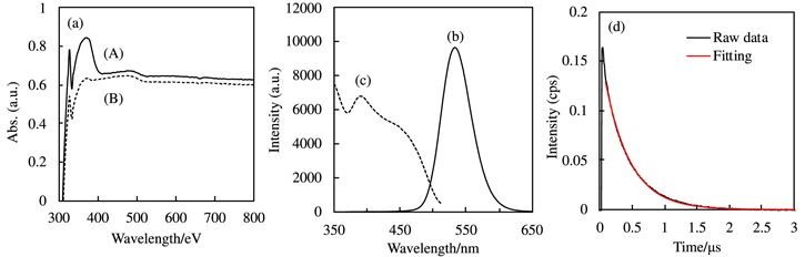
Figure 4. Optical absorption spectra (a) of the SrGa2S4:Eu/ZnO-vnws bilayer (A) and SrGa2S4:Eu layer (B) prepared at 60 V for 30s, emission (b) and the excitation spectra (c), and the decay curve (d) for the 60V-10s bilayer, where the raw data and the fittingcurve were represented with black and red lines, respectively.
Download figure:
Standard image High-resolution imageOnly a visible emission at about 533 nm (excitation wavelength of 320 nm) was observed from the SrGa2S4:Eu/ZnO-vnws bilayer and the SrGa2S4:Eu layer irrespective of the presence of ZnO-vnws and the condition of the electrophoresis deposition. The emission at the wavelength of 533 nm was previously reported to be attributed to the 4f65d→4f7 transition of Eu2+ ions in SrGa2S4:Eu. 22,23 The excitation spectrum (emission wavelength 533 nm) showed a broad form with a peak at around 390 nm. The excitation spectrum with a peak at 278 nm and shoulders at 313 and 391 nm (emission wavelength of 532 nm) was reported for SrGa2S4:Eu containing 2 mol% Eu, 22 and a broad excitation spectrum with a peak at 464 nm (emission wavelength of 538 nm) was reported for Sr1–0.03Ga2S4:Eu0.03. 9 The excitation band at 350 ∼500 nm was assigned to the 4f7 → 4f65d transition of Eu2+ ions in the SrGa2S4:Eu phosphor. 23 While the peak wavelength and the shape of the emission spectrum are almost the same, the peak wavelengths and the shape of the excitation spectra differ greatly among reports. These differences are probably due to differences in measurement conditions, and the associated band structures derived from the composition and coordination environment of the Eu atom. The emission spectrum recorded for a single ZnO-vnws layer under the same conditions showed very low intensities with small emission peaks, as shown in Fig. S2.
The decay and fitting curves were represented by black and red lines in Fig. 4d, and the lifetime was estimated for the decay curve by the following process. The relationship between the intensity and lifetime can be expressed by the following equation, 24
where Y, x, τ are intensity, time, lifetime, and A1 and A2 are constants. The lifetime τ was estimated from the slope of the linear part of the natural logarithm plot between the intensity and time, which was estimated to be 0.389 μs.
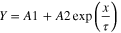
Figure 5 shows the measured X-ray chart image of line profile with the Line and Space (L/S) of 9, 10 15, 20, 45, and 50 μm for the SrGa2S4:Eu/ZnO-vnws bilayer and SrGa2S4:Eu layer by WKα radiation. The line profiles with L/S of 9 ∼50 μm were clearly observed for all the SrGa2S4:Eu/ZnO-vnws bilayer and the SrGa2S4:Eu layer, evidencing that the SrGa2S4:Eu/ZnO-vnws bilayer and SrGa2S4:Eu layer were functioning as scintillators for the X-ray radiation. A line profile of L/S = 6 μm was observed with a ZnO-vnws-free-SrGa2S4:Eu scintillator, as already reported. 10 Since it was difficult to estimate quantitatively the spatial resolution by the detection of the L/S line profile, FWHM values were estimated using the Sigmoid curve-fitting technique for the spatial resolution estimation as shown in Fig. 6a. The blue circles and the orange line respectively represent the raw absorbance value at a given X position and the fitting curve by using the Sigmoid curve. The green line and red dashed line represent the differential curve for the Sigmoid fitting curve and the FWHM, which was used as the spatial resolution.
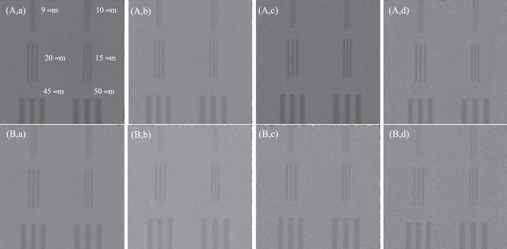
Figure 5. X-ray chart images of SrGa2S4:Eu/ZnO-vnwsbilayers (A) and SrGa2S4:Eu layers (B) prepared at 60 V for 10s (a), 15s (b), 20s (c), and 30s (d). The L/S of the line profiles were 9, 10, 15, 20, 45, and 50 μm, and the same chart was used for all measurements.
Download figure:
Standard image High-resolution image
Figure 6. Line profile and fitting curve (red line) of the SrGa2S4:Eu/ZnO-vnws bilayer prepared at 60 V for 10s (a), and relation between the FWHM values and the thickness (b) of the SrGa2S4:Eu layers for SrGa2S4:Eu/ZnO-vnws (A) and SrGa2S4:Eu (B).
Download figure:
Standard image High-resolution imageFigure 6b shows the relation of the FWHM value on the SrGa2S4:Eu layer thickness for SrGa2S4:Eu/ZnO-vnws bilayer and SrGa2S4:Eu scintillators. The FWHM value decreased with the decrease in SrGa2S4:Eu layer thickness for the SrGa2S4:Eu/ZnO-vnws bilayer scintillator, but the SrGa2S4:Eu scintillator without the ZnO-vnws showed the opposite tendency and showed decreased FWHM value at increased thickness. The reason for the improved FWHM value at increased SrGa2S4:Eu layer thicknesses in the absence of the ZnO-vnws is not clear at present, but it was speculated that the irregularity of the top and bottom interfaces of the SrGa2S4:Eu layer to the Ag layer and GZO/SLG substrate affected the FWHM value at the thin thickness of 6.9 μm, while such detrimental effects were suppressed with the increase in thickness of the SrGa2S4:Eu layer. The SrGa2S4:Eu/ZnO-vnws bilayer scintillator showed the best resolution of 6.8 μm at the SrGa2S4:Eu layer thickness of 6.1 μm, and the best resolution for SrGa2S4:Eu scintillator without the ZnO-vnws was 8.1 μm at the SrGa2S4:Eu layer thickness of 12 μm, indicating the improvement in spatial resolution by introducing the ZnO-vnws. The best spatial resolution for the SrGa2S4:Eu (60 V-10 s)/ZnO-vnws bilayer scintillator was slightly larger than 5.4 μm estimated for the ready-made LuAG scintillator in the same manner. This is thought to be due to the light-guiding effect caused by the ZnO-vnws morphology functioning as an optical waveguide 12 which guided the radial light emitted by SrGa2S4:Eu into unidirectional light. However, the spatial resolution of the SrGa2S4:Eu/ZnO-vnws bilayer scintillator became larger as the thickness of the SrGa2S4:Eu layer increased which then remained almost constant at a corresponding thickness ratio of 1.9 to the ZnO-vnws layer with the SrGa2S4:Eu layer thickness over 10.3 μm. Therefore, the optical guiding effect of the ZnO-vnws layer was more effective when the SrGa2S4:Eu layer was thin. The thickness of the SrGa2S4:Eu layer and the thickness ratio of the SrGa2S4:Eu layer to the length of the ZnO-vnws were speculated to affect the spatial resolution of the bilayer scintillator.
Figure 7 shows the dependence of luminescence intensity and the unit intensity per SrGa2S4:Eu thickness on the thickness of SrGa2S4:Eu for the SrGa2S4:Eu/ZnO-vnws bilayer and the SrGa2S4:Eu layer. The dashed lines in Figs. 7a and 7b represent the linear approximations obtained for the values of SrGa2S4:Eu scintillators. Since the luminescence intensity of the SrGa2S4:Eu/ZnO-vnws bilayer and SrGa2S4:Eu scintillators increased as the thickness of the SrGa2S4:Eu layer increased, the luminescence intensity strongly depended on the thickness of the SrGa2S4:Eu layer. The luminescence intensities of the SrGa2S4:Eu/ZnO-vnws bilayer scintillators were located on or below the approximate lines when the SrGa2S4:Eu thicknesses are over 10.2 μm, but the intensities were located at the upper side of the approximate line below the SrGa2S4:Eu layer thicknesses of ∼7.1 μm. To investigate the effect of the ZnO-vnws introduction on the luminescence intensity, the luminescence intensity per SrGa2S4:Eu thickness, which is abbreviated as unit intensity, was calculated and is shown in Fig. 7b. Since the unit intensity of the SrGa2S4:Eu/ZnO-vnws scintillator was located on or below the approximate line obtained for the ZnO-vnws-free scintillator, the effect of the ZnO-vnws introduction could not be observed for the SrGa2S4:Eu layer thicknesses over 10.3 μm. As the length of the ZnO-vnws was 5.4 μm, the thickness ratio of the SrGa2S4:Eu layer to the ZnO-vnws length was estimated to be 1.9 and 2.9 for 10.3 μm and 15.4 μm in SrGa2S4:Eu thicknesses. The unit intensities were located above the approximate line at layer thicknesses of the SrGa2S4:Eu layer below 7.1 μm, and the effect of the enhancement of the luminescence intensity could be clearly observed with the introduction of the ZnO-vnws. The luminescence intensity was evidently stronger with the introduction of the ZnO-vnws while at the same SrGa2S4:Eu layer thicknesses below 7.1 μm. The thickness ratios were estimated to be 1.1 and 1.3 for the respective thicknesses of the SrGa2S4:Eu layers of 6.1 and 7.1 μm. The effect of the intensity enhancement by the ZnO-vnws introduction appeared at thickness ratios around 1.1 ∼1.3 but disappeared over approximately 2 for the SrGa2S4:Eu/ZnO-vnws bilayer scintillator. The SrGa2S4:Eu/ZnO-vnws bilayer scintillator with the thickness ratios of 1.1 and 1.3 revealed improved resolutions and enhanced intensities, compared to those of ZnO-vnws-free scintillators.
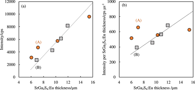
Figure 7. Effect of SrGa2S4:Eu thickness on the luminescence intensity (a) and unit intensity per. SrGa2S4:Eu thickness for the SrGa2S4:Eu/ZnO-vnws bilayers (A) and SrGa2S4 layers (B). The dashed lines represent the linear approximations for the SrGa2S4:Eu layers.
Download figure:
Standard image High-resolution imageFigure 8 shows the schematic illustrations of the light-guiding effects of the ZnO-vnws in the SrGa2S4:Eu/ZnO-vnws bilayer scintillator compared to that of a ZnO-vnws-free SrGa2S4:Eu scintillator, which are described as follows. The absorption coefficient for the 23μm-Eu:CaS/6μm-ZnO-vnws/GZO/SLG was estimated to be 0.87 cm−1 at 59 KeV corresponding to the photon energy of WKα radiation when experimented in a synchrotron radiation facility (SPring-8), as shown in Fig. S3. The absorption coefficient for the SrGa2S4:Eu/ZnO-vnws/GZO/SLG fabricated in this study was not estimated in the same manner, but was speculated to be close to that of the Eu:CaS/ZnO-vnws/GZO/SLG. The WKα radiation at a photon energy of 59 keV was transmitted through the SrGa2S4:Eu/ZnO-vnws bilayer scintillator due to the low absorption coefficient, which caused the SrGa2S4:Eu phosphor particles to emit 533 nm visible light. The emitted lights then propagated radially from the emission point and reached the interface to the ZnO-vnws. The lights penetrating the ZnO-vnws were propagated inside the nanowires by the light-guiding effects. The light-guiding effect of the ZnO-vnws 25 improving the spatial resolution was demonstrated in an X-ray imaging application by comparing to a randomly dispersed ZnO-vnws and a bare substrate without ZnO-vnws. 11 Additionally, P. Yang et al., reported that the ZnO nanowires can generate stimulated emission by light excitation and enhance the excitation light by acting as optical resonators. 26 Since the ZnO-vnws possessed top and bottom interfaces of ZnO/air and ZnO/SLG and the refractive indices are 2.45 for ZnO, 1.45 for SLG, and 1 for air, the interfaces may have acted as partial mirrors which contributed to the function of ZnO-vnws as optical resonators. On the other hand, there was almost no effect on the improvement of the resolution and intensity, when the thickness ratios of the SrGa2S4:Eu layer to the ZnO-vnws were over approximately 2. Further investigations of the effects of the thickness of each layer and the thickness ratios for the bilayer scintillator are needed, but it is evident that the enhancement of the spatial resolution and luminescence intensity by the ZnO-vnws layer is effective when the SrGa2S4:Eu layer is relatively thin.

Figure 8. Schematic illustration of light guiding effect of the ZnO-vnws in SrGa2S4:Eu/ZnO-vnws bilayer (a) in comparison to SrGa2S4:Eu layer (b).
Download figure:
Standard image High-resolution image
Conclusions
SrGa2S4:Eu phosphor/ZnO vertical nanowires (ZnO-vnws) bilayer scintillators were successfully fabricated by electrodeposition of ZnO-vnws followed by electrophoresis deposition of SrGa2S4:Eu particles. The ZnO-vnws were composed of vertically aligned ZnO nanowires with excellent (0001) out-of-plane orientation, and the SrGa2S4:Eu layer was composed of the particles adhered to the ZnO-vnws. The SrGa2S4:Eu/ZnO-vnws bilayer scintillators emitted visible light at a wavelength of 533 nm with a lifetime of 0.389 μs and acted as a scintillator for X-ray irradiation. The resolution and luminescence intensity for SrGa2S4:Eu/ZnO-vnws bilayer scintillators were improved by introducing the ZnO-vnws compared to those of the ZnO-vnws-free SrGa2S4:Eu layer when the thickness ratio of SrGa2S4:Eu layer to ZnO-nws length was constructed at around 1.1 ∼1.3. The SrGa2S4:Eu/ZnO-vnws bilayer scintillator revealed a spatial resolution of 6.8 μm, which was slightly larger than 5.4 μm of a ready-made LuAG single-crystal scintillator. The SrGa2S4:Eu/ZnO-vnws bilayer scintillator with an optimum thickness and thickness ratio is a realistic candidate for a new-generation scintillator with high performance and extended versatility.
Acknowledgments
This work was partly performed under the Strategic Core Technology Advancement Program (Supporting Industry Program, METI (Ministry of Economy, Trade, and Industry)). The synchrotron radiation experiment was performed with the approval of the Japan Synchrotron Radiation Center (JASR), SPring-8 (approval number, 2019A1629).