
Abstract
Using a 3D numerical method, temperatures of pulsed laser annealed epi-Ge layers on SOI and bulk Si substrates are simulated. Epi-Ge is phosphorus-doped by in-situ chemical vapor deposition doping. Both the simulated melt depth and the measured sheet electron density of epi-Ge increases as the laser fluence increases. A strong positive correlation is observed between the simulated melt depth of epi-Ge and the measured sheet electron density. The sheet electron density is calculated using the temperature-dependent solid solubility, while the electron concentration for epi-Ge melted during pulsed laser annealing is assumed to be the liquid solubility of phosphorus at melting point. An intermixing between Ge and Si is observed by cross-sectional transmission electron microscopy, when both Si and epi-Ge are melted in the simulation.
Export citation and abstract BibTeX RIS
Pulsed laser annealing of semiconductors has been the subject of extensive study.1–5 Dopant activation beyond the solid solubility limit can be obtained by laser annealing.6,7 To reduce source/drain resistance, dopant activation of heavily-doped source/drain is essential.8 The time-resolved reflectivity during pulsed excimer laser annealing was used to determine the onset time of melt and melt duration as functions of laser fluences.9 The thermal simulation of laser annealing on Ge or Si substrates can estimate required laser fluences to melt the surface of Ge or Si substrates.9–11 The thermal simulation by the finite-difference method (FDM) is widely used to obtain the temperature during laser annealing.10,12,13 Thermal boundary resistance reduce the effective thermal conductivity.14 Compared to Ge or Si substrates, the thermal boundary resistance at the Ge/Si14 and Si/SiO2 interface15 should be considered in the simulation of laser annealing on epi-Ge on SOI and bulk Si substrates. In this work, temperatures of epi-Ge layers on SOI and bulk Si substrates during pulsed laser annealing process are simulated by a 3D FDM-based simulation. The epi-Ge is phosphorus-doped by in-situ chemical vapor deposition doping. The simulated melt depth is strongly correlated to the measured sheet electron density of epi-Ge. The sheet electron density of epi-Ge is calculated using the temperature-dependent solid solubility.16 The local electron concentration is assumed to be the liquid solubility at melting point if epi-Ge is melted in simulation. As the laser fluence increases, the intermixing between Ge and Si occurs due to the melt of both epi-Ge and Si, as demonstrated by the thermal simulation for the first time.
3D FDM and Experimental
The thermal effect of laser annealing can be described by the 3D heat equation with a source term to represent absorption of light1
![Equation ([1])](https://content.cld.iop.org/journals/2162-8777/6/8/P495/revision1/d0001.gif)
where c is the specific heat, ρ is the mass density, α is the light absorption coefficient, R is the reflectance of Ge, I0(x, y, t) is the intensity, and κ(T) is the thermal conductivity. The simulation scheme of Ref. 10 is used to solve Eq. 1 three dimensionally to understand heating and melting effects induced by laser annealing. The wavelength is 532 nm (Nd:YAG). The laser intensity in time domain is modeled by a Gaussian function. The full-width-at-half-maximum of the laser pulse is 12 ns. The beam size is described by an elliptical Gaussian beam with the major and minor radii of 400 and 10 μm, respectively. The reflectances are 0.5 and 0.74 for crystalline Ge (c-Ge) and liquid Ge (l-Ge), respectively.9,17 The top surface convection coefficient is 10−3 W cm−2 K−1. The ideal heat sinks are imposed by setting the temperatures of all the other boundary surfaces at 30°C except the top surface where is exposed to the laser. The material parameters are listed in Table I.9,10,18–20 Temperature-dependent thermal conductivities of Si, Ge and SiO2 are considered (Table II).20–22 The laser fluence is calculated as, Pavg/(fwxwyπ), where Pavg is average power, f is the repetition rate of 50 kHz, wx and wy are the major and minor radii of the elliptical Gaussian beam. The diffraction of Gaussian beam is ignored due to the Rayleigh range of ∼2 mm much larger than the absorption length of Ge (∼17 nm). The latent heats of Ge and Si are 411 and 1970 J/g, respectively.12 The thermal boundary resistance at Si/Ge and Si/SiO2 interfaces are 3 × 10⁻⁵ 14 and 2.4 × 10⁻⁵ cm2 K/W,15 respectively. The active concentration of phosphorus is considered as23
![Equation ([2])](https://content.cld.iop.org/journals/2162-8777/6/8/P495/revision1/d0002.gif)
where CSSP is the temperature-dependent solid solubility, and CP is the phosphorus concentration in c-Ge. According to the extrapolated solid solubility (∼2.4 × 1019 cm−3 16) at the melting point and the distribution coefficient of phosphorus in Ge (0.0824), the liquid solubility of phosphorus in Ge at the melting point is predicted to be ∼3 × 1020 cm−3. The thicknesses of Si and buried oxide of SOI are 65 and 145 nm, respectively. After HF clean and baking in H2 ambient, the epi-Ge layer with thickness of 110 nm was grown on SOI and the bulk Si substrate by an chemical vapor deposition at 320°C using GeH4 and PH3 as precursors. Experimentally, the sample on a movable stage with a velocity of 6 cm/s was scanned by the pulsed laser. The velocity of the stage is ignored in the simulation since the moving distance during one laser pulse is only ∼1 nm.
Table I. Material parameters used in the simulation.
| c-Si/l-Si | c-Ge/l-Ge | SiO2 | |
|---|---|---|---|
| ρ: density (g/cm3) | 2.3310/2.5220 | 5.3210/5.6-0.625 10−3(T-937°C)20 | 2.2718 |
| c: specific heat capacity (J/g K) | 0.9510/1.0520 | 0.3310/0.4520 | 118 |
| α: absorption coefficient (cm−1) | 1E417/1E69 | 5.7E519/1E69 | 017 |
Table II. Thermal conductivity used in the simulation.
| κ: thermal conductivity (W cm−1 K−1) | |
|---|---|
| c-Si/l-Si | 1.5exp[-0.0027(T-27)], T < 627°C, 0.3exp[-5.2 × 10⁻⁴(T-627)], T ⩾ 627°C21/0.503+2.93 × 10−4(T-1414°C)20 |
| c-Ge/l-Ge | 0.6exp[-0.0022(T-27)], T < 527°C, 0.2exp[-4 × 10⁻⁴(T-527)], T ⩾ 527°C21/0.29720 |
| SiO2 | 9.86 × 10⁻¹¹(T-273)3-1.48 × 10⁻⁷(T-273) 2+8.1 × 10⁻⁵(T-273) -2.4 × 10⁻⁴, T < 727°C 3.14 × 10⁻², T ⩾ 727°C22 |
Results and Discussion
The maximum intensity is 38 MW/cm2 with the laser fluence of 0.22 J/cm2 and the pulse width of 12 ns (Figure 1). The 110-nm-thick epi-Ge layer absorbs most of the light intensity, because of the short absorption length of ∼17 nm. The increase of temperatures in Si and SiO2 is due to heat transfer through conduction. The maximum temperature at epi-Ge surface and also the center of the Gaussian beam reaches 1680°C, a value higher than the melting point of Ge and Si (Figure 1a). The maximum surface temperature of Si on oxide reaches 1450°C. The epi-Ge layer and top portion of Si on oxide are melted. The temperatures of epi-Ge, Si and SiO2 decrease afterwards due to the cooling process and the decreasing laser intensity. The higher temperature of epi-Ge on the SOI than the bulk Si substrate is caused by the large thermal resistance of SiO2. The measured sheet Hall electron density of as-grown epi-Ge on SOI is ∼3.8 × 1013 cm−2 (∼3.5 × 1018 cm−3). The sheet electron density increases as the simulated melt depth of epi-Ge layer increases (Figure 2a). The onset of melt of epi-Ge surface occurs with the laser fluence of ∼0.04 J/cm2. As the melt depth equals to the thickness of the epi-Ge layer (the whole epi-Ge layer is melted), the sheet electron density no longer increases but remains stable at ∼3.3 × 1015 cm−2 (∼3 × 1020 cm−3). Note the epi-Ge thickness is 110 nm. The ∼3 × 1020 cm−3 is the maximum activation dopant concentration obtained by experiments. Si melts for the laser fluence above ∼0.18 J/cm2 (Figure 2a). For epi-Ge on bulk Si, the sheet electron density increases as the melt depth of epi-Ge increases (Figure 2b). Under our sample condition, CP ≫ CSSP, the local active concentration
![Equation ([3])](https://content.cld.iop.org/journals/2162-8777/6/8/P495/revision1/d0003.gif)
The sheet electron density is calculated by integration of C+P over depth. Note that Tmax(z) is the highest temperature at the center of the Gaussian beam during the laser annealing process. Figure 3 shows the cross-sectional transmission electron microscopy (TEM) images of the as-grown epi-Ge on SOI (Figure 3a) and epi-Ge on SOI annealed with laser fluences of 0.15 (Figure 3b) and 0.22 J/cm2 (Figure 3c). The thickness of Si remains the same after the laser fluence of 0.15 J/cm2. The reduction of the thickness of Si from ∼65 to ∼38 nm is due to the intermixing between Ge and Si by the laser fluence of 0.22 J/cm2. The 10-nm decrease of the total thickness of Ge, SiGe and Si layers (Figure 3c) upon annealing at 0.22 J/cm2 is probably due to the evaporation of Ge, which has the surface temperature of 1680°C. The energy-dispersive X-ray spectroscopy (EDS) line scans of annealed epi-Ge on SOI with Ge, Si and O signals are shown in Figure 4. Epi-Ge on SOI annealed with the laser fluence of 0.15 J/cm2 has a sharp boundary between epi-Ge and Si (Figure 4a). With the laser fluence of 0.22 J/cm2, the decreased thickness of the Si layer is ∼27 nm due to the intermixing of melted Si and melted Ge (Figure 4b). Note that the simulated melt depth of the Si layer is ∼30 nm. Most portion of the l-Si layer intermixes with the l-Ge layer and forms SiGe after cooling. The O signal in epi-Ge and Si layers (Figure 4a and 4b) is probably the artifact due to the oxidation of the TEM specimen in the air. The secondary ion mass spectrometry (SIMS) measurement shows that the O concentration of laser annealed epi-Ge on SOI is ∼1 × 1020 cm−3 due to the exposure to the air during laser annealing. The O concentration of as-grown epi-Ge is below the detection limit of ∼1 × 1017 cm−3. The X-ray diffraction (XRD) of as-grown and laser annealed samples are shown in Figure 5. The compressive strain in the as-grown epi-Ge on both SOI and bulk Si substrates is −0.16%. The tensile-strain in epi-Ge is induced by thermal annealing owing to the misfit of thermal expansion coefficients between epi-Ge and Si.25 The tensile strain is 0.32% in epi-Ge on SOI with the laser fluence of 0.15 J/cm2. The XRD broadens for epi-Ge on SOI with the laser fluence of 0.22 J/cm2 due to the intermixing between Ge and Si (Figure 5a). The intermixing occurs when both Ge and underneath Si are melted. For epi-Ge on bulk Si (Figure 5b), no intermixing is observed, since Si remains solid during laser annealing. The tensile strain in epi-Ge on bulk Si is 0.21 and 0.25% after laser annealing with the laser fluence of 0.15 and 0.22 J/cm2, respectively. The atomic force microscopy (AFM) images of as-grown epi-Ge on SOI and annealed by laser fluences of 0.15 and 0.22 J/cm2 are shown in Figure 6. The root mean square (RMS) roughness is 3.6 nm for as-grown epi-Ge on SOI (Figure 6a). The RMS roughness is 3.4 and 2.3 nm after laser annealing with the laser fluence of 0.15 and 0.22 J/cm2, respectively (Figure 6b and 6c).
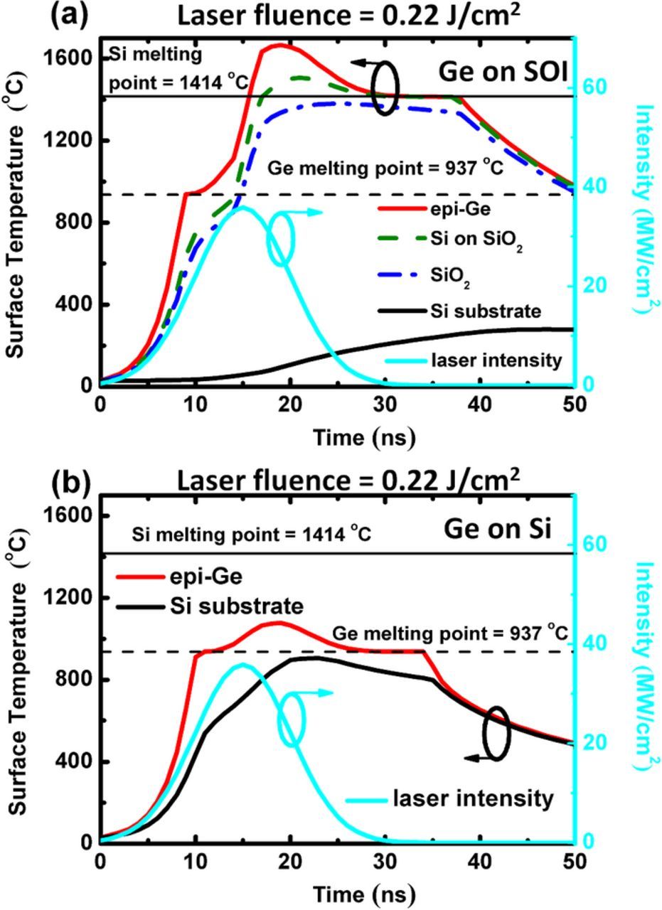
Figure 1. The simulated temperatures of Ge on (a) SOI and (b) bulk Si substrate with the same laser fluence of 0.22 J/cm2.
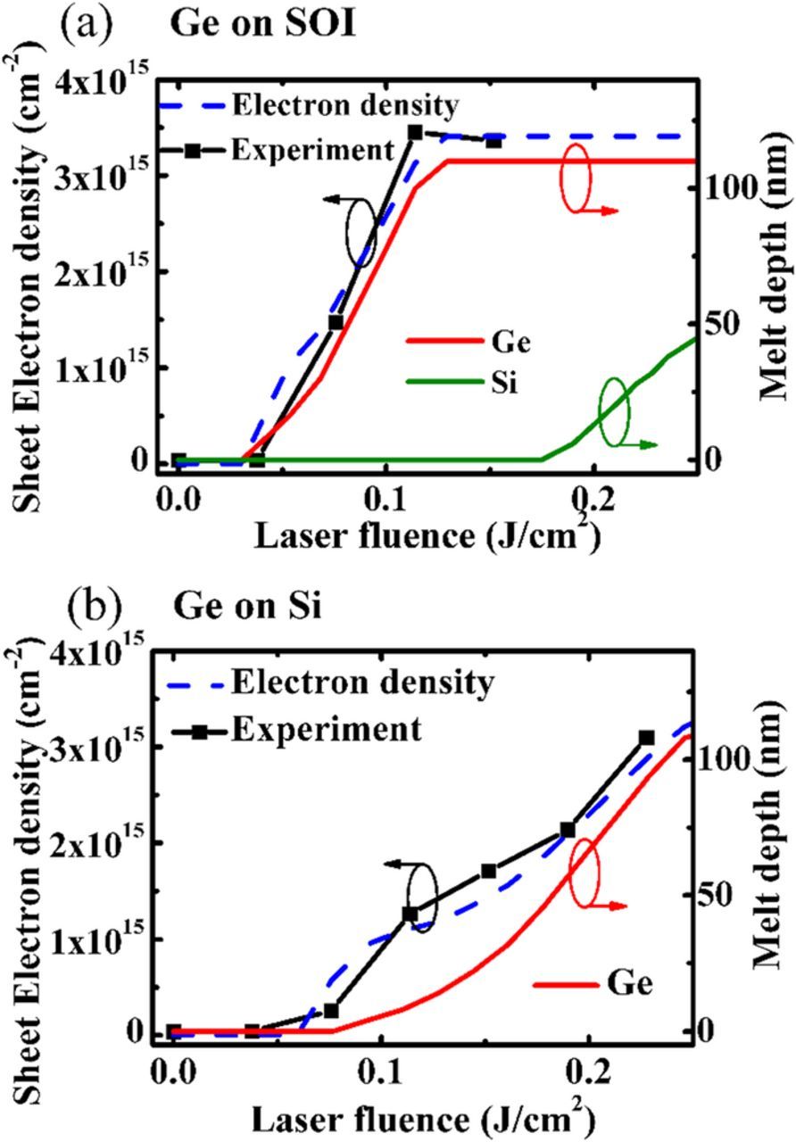
Figure 2. The measured Hall electron concentration and the simulated melt depth of Ge and Si of (a) SOI and (b) bulk Si substrates.
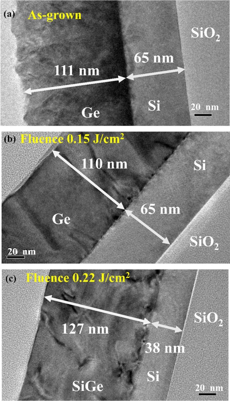
Figure 3. The cross-sectional TEM image of the (a) as-grown epi-Ge on SOI and epi-Ge on SOI annealed by laser fluences of (b) 0.15 and (c) 0.22 J/cm2.
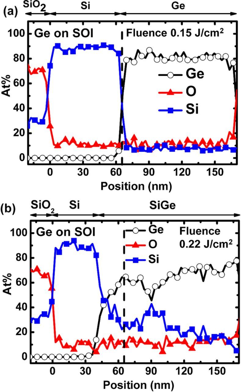
Figure 4. The EDX line scans of Si, Ge, and O in the epi-Ge on SOI annealed by laser fluences of (a) 0.15 and (b) 0.22 J/cm2.
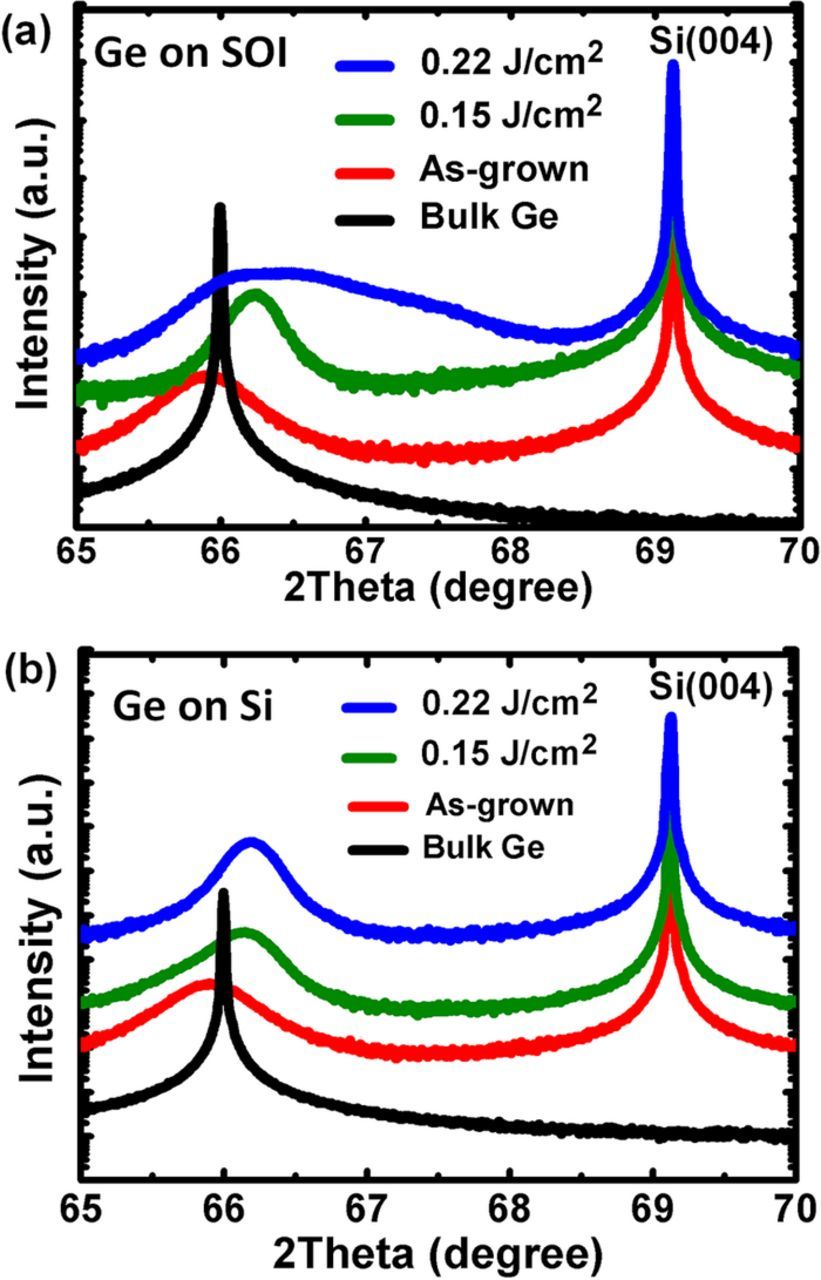
Figure 5. The XRD of as-grown and laser annealed epi-Ge on (a) SOI and (b) bulk Si substrates.
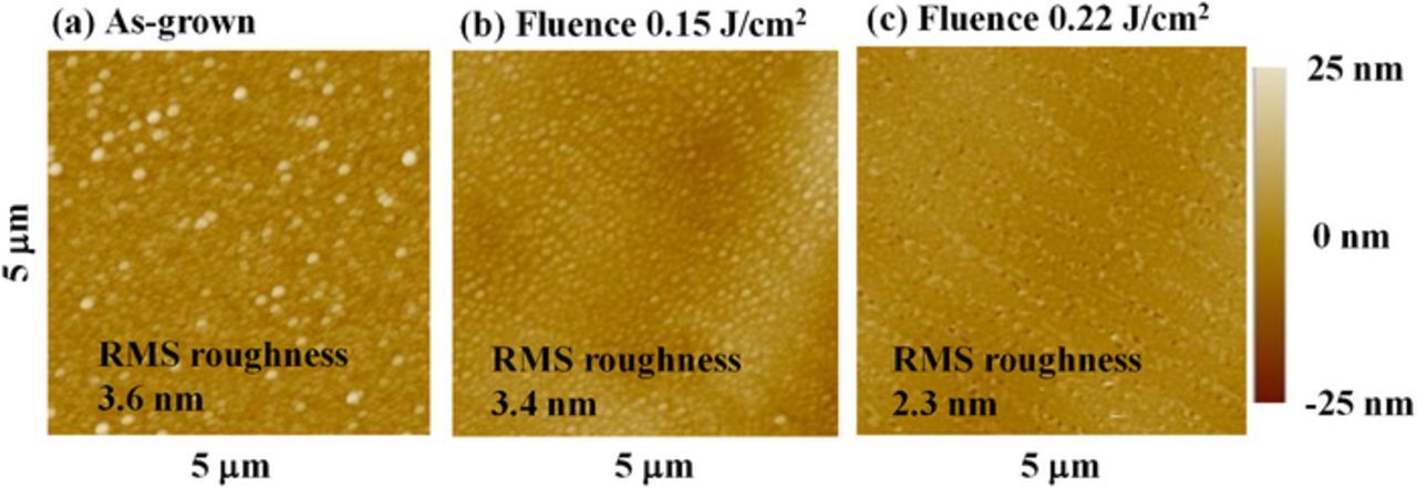
Figure 6. AFM images of 5 × 5 μm2 scan filed of (a) as-grown and laser annealed epi-Ge on SOI with the fluence of (b) 0.15 and (c) 0.22 J/cm2.
Summary
The phosphorus is activated by the melt of epi-Ge layers. The sheet electron density increases as the simulated melt depth of epi-Ge increases. The electron concentration of ∼3 × 1020 cm−3 is the predicted maximum activation concentration. The melt of both Si and epi-Ge results in intermixing between Ge and Si evidenced by TEM and EDS. The simulated temperature of epi-Ge on SOI is larger than bulk Si substrate, due to large thermal resistance of SiO2. The tensile strain induced by laser annealing is due to the misfit of thermal expansion coefficients between epi-Ge and Si. The surface morphology observed by AFM becomes smoother after laser annealing. Our 3D simulation agrees well with the experimental results, and gives the physical insight behind laser annealing in Ge on Si.
Acknowledgments
This work is partially supported by Ministry of Science and Technology, Taiwan, R.O.C. (No. 105-2622-8-002 -001 -, 103-2221-E-002 -253 -MY3, 103-2221-E-002 -232 -MY3, 106-3113-E-492 -001 -CC2) and National Nano Device Laboratories.