Abstract
The ability to achieve near-atomic precision in etching different materials when transferring lithographically defined templates is a requirement of increasing importance for nanoscale structure fabrication in the semiconductor and related industries. The use of ultra-thin gate dielectrics, ultra thin channels, and sub-20 nm film thicknesses in field effect transistors and other devices requires near-atomic scale etching control and selectivity. There is an emerging consensus that as critical dimensions approach the sub-10 nm scale, the need for an etching method corresponding to Atomic Layer Deposition (ALD), i.e. Atomic Layer Etching (ALE), has become essential, and that the more than 30-year quest to complement/replace continuous directional plasma etching (PE) methods for critical applications by a sequence of individual, self-limited surface reaction steps has reached a crucial stage. A key advantage of this approach relative to continuous PE is that it enables optimization of the individual steps with regard to reactant adsorption, self-limited etching, selectivity relative to other materials, and damage of critical surface layers. In this overview we present basic approaches to ALE of materials, discuss similarities/crucial differences relative to thermal and plasma-enhanced ALD, and then review selected results on ALE of materials aimed at pattern transfer. The overview concludes with a discussion of opportunities and challenges ahead.
Export citation and abstract BibTeX RIS

This is an open access article distributed under the terms of the Creative Commons Attribution Non-Commercial No Derivatives 4.0 License (CC BY-NC-ND, http://creativecommons.org/licenses/by-nc-nd/4.0/), which permits non-commercial reuse, distribution, and reproduction in any medium, provided the original work is not changed in any way and is properly cited. For permission for commercial reuse, please email: oa@electrochem.org.
A requirement of increasing importance for nanoscale device fabrication is the ability to achieve atomic scale etching control and materials selectivity during pattern transfer.1–8 An etching method corresponding to Atomic Layer Deposition (ALD), i.e. Atomic Layer Etching (ALE), is expected to satisfy these needs as critical dimensions continue to shrink below the 10 nm scale.
Demonstrations of self-limited dry etching methods capable of near-atomic resolution have a long history in the dry etching community and a brief review will be presented below. Key challenges for these approaches have been specialized equipment, long process times and low throughput.9,10 However, a recent demonstration using a commercial plasma etch tool10 and activities within the dry etching community11 provide indications that the situation has changed, and that we may have reached for ALE the Tipping Point which Gladwell defined as the "the moment of critical mass, the threshold, the boiling point" when "ideas and products and messages and behaviors spread like viruses do".12 This is due to several factors, including unprecedented demands on dry etching technology introduced by the semiconductor device evolution according to Moore's law that can be satisfied by atomic layer etching, advanced capabilities in plasma etch, and the existence of a critical level of information on plasma etch and ALD methods as applied in the semiconductor fabrication space.
In this article we will provide a review of background of these approaches, and focus on issues that have to be overcome for wide-spread implementation in manufacturing.
Technology Demands on Plasma Etch (PE) and Key Shortcomings of Continuous PE Methods
Technology demands
Current semiconductor manufacturing is characterized by the need to mass produce features that are approaching 10 nm critical dimension (CD) and require CD variation of 0.5 nm or less.1,3 The use of ultra-thin gate dielectrics, ultra thin channels, and overall decreasing film thicknesses in combination with more stringent demands on surface property control in field effect transistors, i.e. preventing materials damage, requires control over etching directionality and materials selectivity that approaches the atomic scale.13 Additionally, the material stacks making up devices are becoming more complex and exhibit higher aspect ratios. Examples are 3-dimensional gate etch applications which demand essentially infinite etch selectivity while avoiding introduction of materials damage as FinFETs, Trigates, nanowires and other 3D devices are produced.14–16 For these applications the top of the fin/wire is exposed to the plasma and needs to withstand plasma exposure while the remaining gate is formed around the fin/wire.
The potential of graphene technology has introduced the challenges associated with fabrication of single atomic layer–based technologies.17,18 Gate formation on single atomic layer materials such as graphene requires the ability to stop on a single layer with atomistic precision. Patterning of graphene sheets (ribbons) for digital/logic applications requires line edge roughness (LER) control of <1 nm so that the graphene exhibits semiconducting behavior.19
Shortcomings of continuous plasma etching technology
It will be difficult to meet the above demands of nanotechnological manufacturing using continuous plasma processing approaches for which complex process recipes are used to optimize the achievement of certain process objectives.1 Admitting all reactants simultaneously to the process chamber gives rise to large particle fluxes at certain surface locations through all phases of the plasma process and complex parallel reactions that can evolve with the long-time transients associated with plasma-chamber wall interactions.3,6 For instance, etching selectivity for the prototypical case of fluorocarbon based etching of dielectrics is based on several parallel reactions, which for compositionally distinct materials can lead to different net overall reaction rates, i.e. fairly rapid etching for one material and slow etching or deposition for another material.20–26 However, the thicknesses of these steady-state surface layers can be of the order of several nm. During the time needed for these to form, significant material loss can take place.27 Thick modified surface layers develop on semiconductor and dielectric surfaces that are simultaneously exposed to significant chemical reactant fluxes and ion bombardment.6 To achieve silicon etching directionality in plasma etching for these reactant-rich process conditions, often O2 is added to chlorine- or bromine-based discharges to enhance oxidation of vertical silicon surface features and prevent lateral attack which, however, changes critical dimensions of devices.28 Additionally, profile imperfections, e.g. micro-trenching, can result.
These limitations have resulted in significant developments on pulsed discharges for plasma etching which are promising in overcoming some of these issues.3–6 An alternative and possibly complementary approach corresponds to the reverse of atomic layer deposition technology.
Atomic Layer Deposition and Atomic Layer Etching – General Principles
Atomic layer deposition (ALD)
Atomic layer deposition has become the method of choice for highly conformal coatings in many applications, including advanced semiconductor processing.29–31 The ability to control the thickness of deposited films near one monolayer per process cycle is based on careful choice of chemical precursors which, once adsorbed at one monolayer, passivate the surface and prevent multi-layer adsorption (see Fig. 1). This is followed by a reaction step which transforms the precursor on the heated substrate into the desired material. An example is the deposition of an Al metallorganic monolayer which upon oxidation is transformed into Al2O3.32–35 Deposition conformality is a key objective of many ALD processes. It can be successfully achieved even for very challenging geometrical situations, e.g. high-aspect ratio trench or via structures, since self-limited adsorption is insensitive to local variations in incident particle fluxes at surface locations.

Figure 1. Schematic of one cycle of a typical ALD process to produce thin Al2O3layers (redrawn after Potts and Kessels37). The surface modification step ((b)-(d)) is based on self-limited adsorption of a reactive precursor, followed by pump-out. The steps ((e)-(f)) involve exposure to an oxidizing gas, e.g. water, O2 plasma, etc, followed by pump-out and transform the precursor layer into roughly a monolayer of the final Al2O3 material. For the substrate (g) obtained after one ALD cycle, the steps (b) through (f) will be repeated. The overall deposited layer thickness is produced by n ALD cycles.
For thermal ALD processes the activation energy for the chemical reaction that takes place during the reaction step is provided by substrate heating. Thermal ALD rates drop off at low substrate temperature when the thermal energy becomes insufficient to drive the chemical reaction. The possible substrate temperature range over which an ALD window exists is limited at low temperature by incomplete reaction during the reaction step or multi-layer condensation during precursor deposition29 (see Fig. 2). The ALD window is limited at high substrate temperature by thermal decomposition of precursors, thermal desorption, and other loss processes.29

Figure 2. Schematic illustrating the thermal "ALD window" concept (redrawn after George29).
Plasma-enhanced ALD
Recently, there has been strong growth in plasma-enhanced ALD that uses plasma-generated radicals/energetic species during the reaction step to enable or speed up chemical reactions with the deposited precursor layer that are either too slow or not possible with just thermal energy and typical reactants. The reviews36–38 describe key features of plasma-enhanced ALD, and differences relative to thermal ALD. Plasma-assisted ALD offers greater processing flexibility relative to thermal ALD, including a larger number of precursors that may be used, the opportunity to use lower substrate temperatures than possible in thermal ALD while maintaining growth per cycle, and an increased range of materials that may be deposited along with control of materials properties. One limitation of plasma-assisted ALD is reduced conformality (step coverage) relative to thermal ALD when coating substrates with pronounced surface topography,36 e.g. high aspect ratio trenches or holes. This is explained by the highly reactive species created in the plasma environment which make the achievement of self-limitation more difficult, i.e. it has been observed that deposition on passivated surfaces can take place more easily in the plasma environment.36,39 The result is that process rates may become more strongly dependent on the locally available chemical precursor flux, and may be controlled by radical recombination loss probabilities in deep trenches,39 and/or energy flux, in contrast to ideal ALD processes. Profijt et al.36 also point out additional concerns for plasma-based ALD processes, e.g. vacuum ultraviolet (VUV) induced electrical damage to insulators which is absent in a purely thermal environment. These features of plasma-enhanced ALD are expected to be also very important for plasma-based atomic layer etching methods.
Atomic layer etching (ALE)
Similar to ALD, realization of ALE has long been based on replacing the complex plasma-surface interactions of steady-state plasma etching by a sequence of individual, self-limited surface reactions (see Fig. 3). In a first reaction step, a chemical precursor is introduced into the reactor and adsorbed at the surface of the substrate. The precursor is chosen so that upon reaction with substrate atoms volatile products can be formed. Conditions must be chosen so that the precursor does not spontaneously etch the substrate, e.g. by lowering the substrate temperature. Ideally, reactants are present at the active surface at about a monolayer. Subsequently, the chamber is exhausted to remove remaining chemical reactants.

Figure 3. Schematic of one cycle of a typical ALE process. The surface modification step ((b)-(d)) may include self-limited adsorption, short deposition, etc, followed by pump-out. Low energy Ar ion bombardment is often used for selective removal of reacted region ((e),(f)). For the substrate (g) after one ALE cycle, the steps (b) through (f) will be repeated. The overall etch depth is produced by n ALE cycles.
In a second surface reaction step, bombardment of the surface with energetic species, typically a beam of low energy ions,9 provides the necessary energy to induce chemical reactions between the adsorbed species and the substrate. Other methods employed for inducing a reaction of adsorbed species with substrate atoms to produce volatile products are bombardment with fast neutral atoms,40–42 electrons,43 or irradiation with photons.44 (Isotropic atomic layer etching based on thermal product desorption has been described,45 but these thermal approaches necessitating elevated substrate temperatures will not be discussed extensively in this review.) To minimize physical sputtering and surface damage, energies for ion or neutral beam bombardment are typically limited to 100 eV or lower. The reaction chamber may be evacuated again to complete one cycle. The ALE process ideally proceeds in a cyclic, self-limiting way, with a substrate thickness loss of about 1 monolayer per cycle.
ALE window
To control the thickness loss (etch depth) per cycle, self-limited surface reactions are required. Both spontaneous chemical etching by the precursor and physical sputtering should be minimal. The concept of an ALE window located between the spontaneous chemical etching and the physical sputtering regimes is schematically illustrated in Fig. 4 for ion-induced etching. The key parameter for ALE that plays a similar role as substrate temperature in thermal ALD is ion energy. In a similar fashion as there exists an ALD window versus substrate temperature, there is an ALE window versus ion energy. In a plasma environment, ions with an energy distribution are incident on the substrate and control physical sputtering and substrate damage extent. Bombardment of the surface between chemical reactant exposures at a sufficiently high fluence is assumed in Fig. 4. The modification of the surface by the precursor allows the material to be etched with lower activation energy as compared to the underlying material without modification.9 The presence of chemical reactants at the substrate surface along with ion bombardment induce a chemical reaction between the surface atoms and the precursor which causes etch products to boil off or sputter from the surface. This process enables directional etching of the material at ion energies above the chemically enhanced etching energy threshold Eceth and below the physical sputtering energy threshold Epsth, respectively. By carefully tailoring the energy of ion bombardment, it is possible to control the etching depth to about a monolayer. Spontaneous chemical etching of the reactant/substrate system interferes with this approach and the thermal energy required to drive these reactions is made negligible by reducing the temperature of the substrate sufficiently. While Fig. 4 illustrates this concept for ion bombardment, in the literature ALE windows have also been demonstrated by using electron, fast neutral and photon bombardment of surfaces for directed energy input.

Figure 4. Schematic illustrating the concept of an "ALE window" located between the spontaneous chemical etching and the physical sputtering regimes. The presence of chemical reactant on the substrate surface enables directional etching of the material in a window of ion energies above the chemically enhanced etching energy threshold Eceth and below the physical sputtering energy threshold Epsth, respectively. Spontaneous chemical etching of the reactant/substrate system interferes with this approach and is made negligible by reducing the temperature of the substrate sufficiently.
An important question relates to the degree to which ion energy and the width of the distribution of ion energies must be controlled. While average ion energy has been shown to be useful,9 careful studies of the impact of ion energy distributions on ALE performance are required to answer the question how closely ion energies must be controlled to enable optimal exploitation of the ALE window. Shin et al.46 investigated nearly mono-energetic ion energy distributions (IEDs) and observed novel phenomena (see below).
Critical neutral exposure and critical dose for energetic particle bombardment
In order for the etching depth per cycle to be self-limited, the chemical reactant exposure of the substrate has to be sufficiently high to achieve surface saturation, and the dose of low energy particles received during a cycle has to be balanced with this and also be sufficiently high. Figure 5 schematically shows the impact of different chemical reactant exposure conditions, e.g. by changing reactant pressure, on the thickness loss depth per cycle. Ample energy input to the surface by low energy particle bombardment within the ALE energy window at a sufficiently high dose between chemical reactant exposures is assumed. The lower values of these have been termed critical exposure, i.e. pressure * time of chemical reactant, and critical dose (for energetic particle bombardment), respectively. For instance, self-limited etching of HfO2 at 1 ML/cycle using BCl3 and energetic Ar neutral beam bombardment required a BCl3 pressure above a critical pressure of 0.22 mTorr for 20 s BCl3 exposure and a critical dose for energetic particle bombardment of 1.48×10¹⁷ atoms/cm2, respectively.47 Corresponding information has been published for other reactant/materials systems.

Figure 5. Schematic illustration of the dependence of etched thickness per cycle on exposure time for different pressures ((i) – lowest pressure, (ii) - intermediate and (iii) – highest) and assuming negligible spontaneous etching. Self-limitation requires saturation surface coverage which at the highest pressure (iii) is achieved after the shortest exposure time. Alternatively, a plasma and production of radicals may be used to reduce the time required to achieve saturation surface coverage.
One key need driving development of ALE approaches is the achievement of atomic scale etching selectivity with regard to a different material. More generally, owing to the complex nature of surfaces in advanced semiconductor devices, simultaneous etching control over multiple materials is typically required. By working close to the energy threshold for physical sputtering of one material, and exploiting energy threshold differences among different materials, etching selectivity can be optimized.9 The threshold energy for physical sputtering Epsth depends on the nature of the material and is higher in the case of SiO2 than for Si, Epsth(SiO2)>Epsth(Si). By supplying chemical reactant to the substrate surface, chemically enhanced etching is possible, with an energy threshold Eceth(SiO2) that is lower than for physical sputtering Epsth(Si), which may enable selective etching of SiO2 over Si. The amount of material etched per cycle will depend on the surface coverage of the chemical reactants up to a saturation coverage. In the schematic of Fig. 4 it is also assumed that in this ALE window between Eceth and Epsth the substrate thickness loss per cycle is determined by the reactant coverage and essentially independent of ion energy, which does not need to be the case.
Maintaining etching directionality, achieving dimensional control approaching atomic scale, and leaving materials after ALE damage-free are other essential objectives.
An important advantage of a cyclic ALE process relative to continuous etching is that it provides the opportunity to decouple the reaction steps and through detailed study of each, establish how variations of incident particle parameters (chemistry, energies, etc.) enables product volatilization, self-limiting behavior and protection of lateral and vertical surfaces/underlayers that are consistent with the requirements on the overall process.
Although ALE shows some similarities to ALD with regard to physisorption/chemisorption requirements at the surface, the requirements with regard to "volatile product" removal are fundamentally different. Whereas for ALD, films are grown in a conformal fashion, for ALE the "etch product" removal ideally should take place in a directional fashion. Because of this fundamental difference from ALD, ALE provides profound surface chemistry challenges and energetic species/surface interaction problems that are special.
Atomic Layer Etching of Various Materials – A Brief Survey
As discussed, the study of ALE technology goes back more than 30 years. A multitude of different kinds of approaches have been applied to ALE of GaAs and silicon along with a significant number of other materials. In concert with the large number of approaches and methods, these approaches have been referred to by many different names, including atomic layer etching, molecular layer etching, digital etching, layer-by-layer etching and others. To make it easier to obtain an overview of this literature, we provide in Table I a brief listing of published work on materials and approaches for which atomic layer etching has been investigated using both experimental and theoretical methods. Essential information extracted from the publications is presented below. For halogen-based etching of GaAs,48–50 silicon51–56 and other materials there is a large body of atomistic etching work not aimed at pattern transfer and replacement of plasma etching methods. This literature provides important atomic layer etching and surface chemistry background, but is not reviewed. For instance, Maki and Ehrlich57 described laser-induced bilayer etching of GaAs at the Angstrom and sub-Angstrom level in 1989, but their work addressed a different application. Wet etching methods have also not been covered.
Table I. Overview of materials and ALE investigations.
| Material | Precursor Chemistries for Adsorption | Energy Source for Etching/Desorption | Reference |
|---|---|---|---|
| Al2O3 | BCl3 | Ar neutral beam | 59 |
| Al2O3 | BCl3 | Ar neutral beam | 58 |
| BeO | BCl3 | Ar neutral beam | 60 |
| III-V: GaAs | Cl2 | Electron bombardment | 43 |
| III-V: GaAs | Cl2 | low-energy Ar+ ions | 61–63 |
| III-V: GaAs | Cl2 | 248 nm KrF excimer laser and Ti sapphire laser | 44,64 |
| III-V: GaAs | Cl2/Ar plasma | Ar ions from ECR plasma | 65 |
| III-V: GaAs, | Cl2/Ar plasma | Ar ions from ECR plasma | 66 |
| III-V: GaAs | Cl2 | Ne neutral beam | 67 |
| III-V: InP | Tertiarybutylphosphine | Halogen lamp desorption | 68 |
| III-V: InP (and InAlAs, InGaAs) | Cl2 | Ne neutral beam | 69–71 |
| Ge | Cl2 | Ar ions from ECR plasma | 72 |
| Ge (and Si, SiGe) | Cl2 | Ar ions from ECR plasma | 73 |
| Graphene | O2 plasma | Ar neutral beam | 74 |
| Graphite | O2 plasma | Ar neutral beam | 75 |
| HfO2 | BCl3 | Ar neutral beam | 47,76 |
| HfO2 | Cl2 | Ar neutral beam | 77 |
| Polymer (Polystyrene) | O2 | Ar ions from CCP plasma | 78 |
| Si | CF4+O2 plasma | Ar ions from ECR plasma | 79 |
| Si | CF4/O2, NF3/N2, or F2/He plasmas | Ar ions from ECR plasma | 80 |
| Si | Cl2 | Ar ions from ECR plasma | 83 |
| Si | Cl2 | Ar ions from ECR plasma | 84 |
| Si | Cl2 | 50 eV Ar ions (MD simulation) | 85 |
| Si | Cl2 | Ar ions from helical resonator plasma | 86 |
| Si | Cl2 | Ar ions from helicon plasma | 87,88 |
| Si | Cl2 | Ar ions from ICP type ion gun | 89 |
| Si | Cl2 | Ar neutral beam | 40,41,90,91 |
| Si | Cl2 | Ar or He ions from ICP source | 92 |
| Si | Cl2/Ar plasma | Ar ions from ICP source | 9 |
| Si | Cl2/Ar plasma | Ar ions from ICP source | 10 |
| Si3N4 | H2 plasma | Ion bombardment from Ar/H2 ECR plasma | 93 |
| Si3N4 | Ion implantation from H2 plasma | Wet etching (aqueous HF solution) | 94 |
| SiO2 (and Si) | CFx+ ions or radical adsorption | Ar ions (MD simulation) | 95 |
| SiO2 | C4F8 /Ar plasma | Ion bombardment from C4F8/Ar ICP plasma | 9 |
| SiO2 | C4F8 /Ar plasma | Ar ions from magnetically enhanced plasma | 9 |
| SiO2 | C4F8/Ar plasma | Ar ions from ICP source | 99 |
| TiO2 | BCl3 | Ar neutral beam | 105 |
| ZrO2 | BCl3 | Ar neutral beam | 106 |
Table I lists materials in alphabetical order, and references for a given material are sorted primarily according to the year published. We apologize in advance for mistakes, omissions and redundancies of Table I.
Al2O3 and Be-Oxide
ALE studies on Al2O358,59 and Be-oxide on GaAs substrate60 were performed by Yeom's group using a neutral beam system that is based on an ICP source, for which accelerated Ar+ ions are neutralized by low angle forward reflection from a surface. They used up to 30 s BCl3 gas exposure for adsorbing chlorine reactants at the surface, followed by evacuation, striking a plasma and bombarding the passivated surface with a neutralized Ar beam at 100 eV. Measured etch depths per cycle were about 1 Angstrom. They also describe results of density functional theory for the interaction of BCl3 with Al2O3 which they thought provided insights that could be exemplary for other ALE systems as well.58 For BeO on GaAs negligible sputtering was seen for bombardment energies of less than 130 eV, and a self-limited etch depth of 0.75 Å/cycle at saturation.
III-V: GaAs, InP, InAlAs, InGaAs and others
Atomic layer etching of III-V materials is among the oldest ALE demonstrations. Meguro et al. in 199043 used exposure of GaAs to Cl2 gas and electron bombardment at 100 eV to demonstrate a self-limited iterative etching approach. They achieved about 1/3 ML etching per cycle. This work demonstrated clearly that the etching was limited by the adsorption of the chemical reactant. In related work they also evaluated surface activation using low energy Ar ion bombardment using an electron beam excited plasma.61,62 They published subsequently additional work using Ar ion bombardment,63 or photon irradiation of a chlorine-coated GaAs surface.44,64 Aoyagi et al.65 studied GaAs ALE using alternating Cl2 exposure and synchronized low energy Ar+ bombardment by applying a low bias voltage in an electron cyclotron resonance (ECR) plasma system. The ECR Ar discharge was continuously maintained, and Cl2 was admitted for times up to 40 s to achieve adsorption of Cl atoms at the GaAs surface. They report self-limited etching of about a monolayer per cycle for a certain exposure time window of the substrate to the chlorine discharge and the low energy Ar ion beam. For extended exposure times (greater than 20 s), the etch depth per cycle decreased which they explained by multi-layer Cl adsorption. Ko et al.66 also examined layer-by-layer etching of GaAs, InP, GaInAs, and AlInAs using Cl radicals produced by a low power discharge and Ar+ ion bombardment (with additional RF bias) produced sequentially in an ECR system. For complete chlorine surface coverage of GaAs achieved by 6 s exposure to an Ar/Cl2 discharge at 1 mTorr they observed self-limited etching of about 5 A/cycle. For their approach they quote a typical cycle time of 45 s, which consists of 10 s reactive radical adsorption time, followed by pump out of excess radicals (30 s), and a desorption time with Ar ions of 5 s. This shows the strong impact of the purge cycle on cycling time. In another study, Lim et al.67 used Cl2 exposure of GaAs and a Ne neutral beam source and measured about one atomic layer/cycle.
When Ko et al. studied layer-by-layer etching of InP they found that sample heating to 150°C and a higher RF bias than for GaAs was required to observe etching.66 Etching of InP was studied by Otsuka et al.68 using brief exposures to tertiarybutylphosphine, pump-out followed by substrate heating using a halogen lamp for desorption of products. This resulted in etch depths of a fraction of an Angstrom per cycle.
Park et al.69,70 studied ALE of InP and InAlAs based on 20 s exposure to Cl2 at 0.4 mTorr, followed by Ne neutral beam bombardment. They measured roughly 1 monolayer /cycle (1.47 A/cycle) for InP with high selectivity against InAlAs (0.02 A/cycle), and observed no significant surface compositional changes. This ALE approach was applied by Kim et al.71 for fabrication of InAlAs/InGaAs high electron mobility transistors. Changes in surface stoichiometry and surface roughness were investigated in several of the studies on compound semiconductors, and ALE methods generally appeared promising with regard to minimizing changes in these surface properties.
Germanium
Sugiyama et al.72 studied ALE of Ge based on alternating Cl2 exposure and Ar+ ion bombardment using an ECR system. Importantly, they found that they could not inject Cl2 into an ECR plasma, since the plasma-generated Cl radicals etched the Ge spontaneously, whereas this was not the case for Si. They report 1.5 A/cycle for longer Ar+ irradiation and higher microwave power, and stated that Ar+ ions with an energy higher than ∼13 eV were effective for etching. Similarly, Matsuura et al.73 investigated ALE of Ge, Si, and SiGe using Cl2 without plasma followed by low energy Ar+ bombardment in an ECR system. For extended Ar+ ion bombardment and chlorine surface saturation they measured an etch rate per cycle that approached an atomic-layer thickness. Ge was found to be more reactive than Si since it approaches more rapidly saturation of surface chlorination.
Graphene, graphite
Lim et al.74 performed ALE of graphene using an oxygen plasma for exposure of graphene to O radicals (5 min), followed by energetic Ar neutrals beam exposure (1 min). They measured removal of one graphene layer per cycle. They also discussed graphene damage issues, and damage annealing. Similarly, Kim et al.75 applied this approach to etching of graphite, and measured removal of 1 monolayer per etching cycle.
HfO2
Park et al.47,76 studied ALE of HfO2 using adsorption of BCl3 followed by neutral beam bombardment. They observed self-limited etching of 1.2 A/cycle which required specific BCl3 exposure and neutral beam dose. No etching was observed when using Cl2 instead of BCl3 for the pressures investigated (up to 0.35 mTorr). On the other hand, Min et al.77 report HfO2 etching using Cl2 and neutral Ar beam etching at less than 1.0 A/cycle, with high selectivity against an SiO2 underlayer. The reason for this difference was not discussed.
Polymer
Vogli et al.78 used a polystyrene-based photoresist material to demonstrate Angstrom layer removal of polymer in a capacitively coupled plasma system. One cycle consisted of O2 exposure of the polymer material to adsorb species, O2 exhaust from the chamber, Ar ion bombardment using low ion energies (∼20 eV) to remove oxygen-associated carbon from the surface, followed by Ar exhaust. Molecular oxygen does not spontaneously react with polymers at room temperature and can be adsorbed on an activated polymer surface to form a monolayer of oxidized carbon material over unmodified polymer surface atoms. This work demonstrated that about 1.3 Å of unmodified material could be removed per step, but also illustrated the unexpected complexity of ALE processes. The key to the success of this process was the deposition of a thin (∼1 Å) reactive layer of polyimide-related film precursors inadvertently sputtered from a second electrode within the etching chamber. The polyimide-related deposition inhibited etching during the Ar ion bombardment step once the oxygen-associated reactive layer had been removed. Additionally, the deposition of this ultra-thin layer increased O2 adsorption during the O2 gas exposure step.
Silicon
For the F/Si system spontaneous etching that takes place at room temperature can be suppressed by using cryogenic temperatures. Horiike et al.79 studied ALE of silicon and used exposure to a fluorine-based plasma for the formation of an SiFx adsorbate layer. This was followed by bombardment with Ar ions of approximately 20 eV generated by an ECR plasma to desorb SiFx reaction products. By careful choice of parameters, e.g. flow rate, atom mole fraction of halogen gases, exposure time, bias voltage, and cooling of the substrate to 113 K to decrease spontaneous chemical etching of silicon, they obtained an etching rate of approximately 1.5 A/cycle, close to a monolayer and indicative of approximately self-limiting etching. Sakaue et al.80 used a similar approach to achieve atomic layer etching of cooled silicon using exposures to different fluorine-based discharges. They observed that the amount of physisorbed fluorine molecules on Si surfaces controls the self-limited etching rate which varied between 2.5–8 A/cycle. They also found that the etching of Si with a 20 nm pattern width PMMA mask was anisotropic and the Si etching rate was five times larger than the etching rate of PMMA during this process, demonstrating that atomic layer etching can be a selective approach.
Cl2/Si system
A great deal of ALE work has focused on the Cl2/Si system at room temperature since the saturation adsorption characteristics of Cl2 on silicon followed by energetic ion bombardment are favorable to achieving self-limited ALE. For chlorine adsorption on a room temperature silicon substrate, Langmuir self-limited adsorption of about one monolayer of chlorine is typically seen.81,82 Matsuura et al.83 found a self-limited layer-by-layer etching mechanism with the substrate at room temperature using Cl2 exposure followed by low energy (20 eV) Ar ion bombardment in an ECR system. An etch depth of 0.5 atomic layer per cycle was achieved which increased with Cl2 exposure of the surface. Suzue et al.84 also used Cl2 exposure and low energy ion bombardment from an ECR plasma to examine the substrate orientation dependence of Si ALE. They found that the sticking probabilities of chlorine radicals were almost independent of the substrate orientation.
The group of Economou performed both modeling85 and experimental work86 on Cl2/Ar+ based ALE of silicon. Molecular dynamics simulations of Si ALE by Athavale et al.85 using 50 eV argon ion bombardment of Si(100) passivated with a monolayer of adsorbed chlorine showed that 93% of etched Si originated from the top silicon layer and 7% from the underlayer. For 50 eV Ar+ ions the Si reaction yield was 0.172 Si atoms removed per ion, 84% in the form of SiCl, 8% elemental Si and 8% as SiCl2. These results nicely demonstrate the concept of the ALE window, since this yield is higher than expected for physical sputtering. They also discussed introduction of structural damage in the top three silicon layers. In their experimental work86 they used a helical resonator plasma source to achieve ALE of silicon by Cl2 exposure and low energy Ar ion bombardment. They observed a self-limiting process with respect to both Cl2 and ion dose, and concluded that control of the ion energy was the most important factor in realizing ALE.
Kim et al.87,88 performed ALE of Si using Cl2 and low energy Ar bombardment (∼30 eV) using a helicon plasma and employing a shutter for process control. They measured etch depths of about 0.7 A/cycle. Park et al.89 performed Si ALE using Cl2 exposure for 20 s followed by Ar ion bombardment at ion energies in the range of 70 to 90 eV to observe self-limited etching at 1.36 A/cycle. Subsequently, Yeom's group developed this approach to perform Si ALE using the same kind of Cl2 exposure in combination with energetic Ar neutrals obtained by the low-angle forward reflection neutral beam technique.40,41,90,91 They observed a self-limited Si etch rate of a monolayer per cycle for both Si (100) and Si (111) orientations when Cl2 and Ar neutrals were supplied above the critical dose values, and surface roughness that remained very low and comparable to a reference sample without ALE.
Yun et al.92 studied ALE of poly-Si using Cl2 exposure and either Ar or He low energy bombardment. They observed self-limited etching of 0.8 A/cycle for Ar, and 0.6 A/cycle for He, with a process window that was much greater for He than Ar ion bombardment.
Agarwal and Kushner9 addressed the question if Si ALE can be performed in conventional plasma etching equipment, e.g. an ICP etching system for directional Si etching. In their computational study of Si ALE they modeled an inductively coupled plasma where Cl2/Ar without bias of the Si substrate is used for chlorine passivation of the Si surface. During the passivation step, Cl+ is the dominant ion and ion energies are below 20 eV. The chlorination of the surface is due to neutral Cl atoms formed by the plasma, which at the 20 mTorr pressure used proceeds rapidly and does not produce multiple layers of passivation since diffusion of Cl into the Si is slow. This is followed by a second cycle in which a pure Ar plasma and biasing is used to etch the passivated Si. During the etching step, Ar+ ion energies are between 50 and 60 eV, and observed etch rates were about 1 ML/cycle. One conclusion of this work was that an essential prerequisite for achieving ALE performance of Si are control of the Ar/Cl2 chemistry along with ion energy and angular distribution (IEAD) functions. This approach has significant potential to speed up processing relative to ALE based on halogenation of Si using simply gaseous halogens, e.g. Cl2.
Recently, Kanarik et al.10 realized this ALE approach in an ICP reactor equipped with fast gas-switching capabilities to achieve short process cycles. Rapid surface chlorination using an Ar/Cl2 plasma, rapid pump-out to establish a pure Ar plasma and RF biasing for efficient product desorption were discussed as key to achieve practical ALE cycle times. The ALE process was reported to consist of self-limiting cycles which yielded an etched Si surface that was smoother and showed no microtrenching as compared to Si etched using a continuous plasma etching process.
Si3N4
Matsuura et al.93 proposed layer by layer etching of Si3N4 by using a remote H2 ECR plasma. The interaction of hydrogen atoms with the Si3N4 surface removed N atoms from the outermost surface of the Si3N4. This was followed by bombardment of the modified surface using Ar and hydrogen ions. Posseme et al.94 evaluated a thin layer etching method based on low energy ion implantation of the Si3N4 surface using an H2 plasma. The modified Si3N4 surface layer could be selectively removed using wet etching. The modified surface layer had a typical extent of about 10 to 20 nm in this work, due to the projected range of hydrogen ions, and thus was significantly greater than typical layer thicknesses removed by ALE processes.
SiO2
For atomic layer etching of SiO2 using fluorocarbon ions or precursors, computational work has been performed by Rauf et al.95 and Agarwal and Kushner.9 The molecular dynamics simulation of Rauf et al.95 first showed potential of a two-step etch process consisting of the formation of a nanometer-thick, self-limited fluorocarbon passivation layer on an SiO2 or Si surface followed by etching with Ar+ ions with energies up to 50 eV using the deposited fluorocarbon as a source of etchant. A sequence of these steps enabled nanometer precise etching of SiO2 and Si.
Agarwal and Kushner9 examined ALE of SiO2 using C4F8/Ar in a capacitively coupled plasma (CCP) reactor. Their work was motivated by the observation that because of the use of different gas mixtures for the passivation and etching steps and the need to exhaust the reaction chamber, ALE results in an inherently slow etch rate. They argued that during actual device fabrication the switch to an ALE method would likely only be implemented after a conventional rapid plasma etching process had thinned the material to a few monolayers above the interface between materials. Such an approach could be realized using separate, dedicated plasma etching and ALE processing chambers. This is undesirable, since it is expensive from several points of view and requires additional wafer handling. Alternatively, if one could perform both main etch and atomic layer etching in the same conventional plasma reactor, cost and processing time would be reduced. Since a limitation of these approaches with respect to throughput is the existence of purge steps, Agarwal and Kushner9 also examined the question if elimination of the purge steps is possible and self-limited etching can be achieved if the entire SiO2 etching cycle is performed using a single gas mixture, and simply controlling ion bombardment energies during a cycle by changing RF bias. By utilizing a nonsinusoidal bias waveform,96,97 they controlled ion energy distribution functions, and demonstrated self-limiting etching at 1 to several ML/cycle. This method is related to pulsed plasma approaches.5,98
Using a steady-state Ar plasma in conjunction with periodic injection of a defined number of C4F8 molecules and synchronized plasma-based Ar+ ion bombardment, Metzler et al.99 evaluated an approach related to both simulations9,95 and demonstrated that in agreement with the simulations Angstrom level precision in etching of SiO2 is possible. For low energy Ar+ ion bombardment conditions giving a maximum ion energy of about 20 eV, the physical sputter rate of SiO2 vanishes. Conversely, for the same ion energies and a SiO2 surface coated with several Angstroms of fluorocarbon (FC), SiO2 etching is initiated, and stops once the FC supply is exhausted. Precise management of C4F8 supply enables control of the deposited FC layer thickness in the 1 to several Angstrom range. The temporal variation of FC deposition, FC and SiO2 etching for Ar+ ion energies of 25 eV for this process during a number of cycles is shown in Fig. 6. As the fluorocarbon surface coverage decreases, the SiO2 ER vanishes, which enables controlled removal of Angstrom-thick SiO2 layers per cycle.

Figure 6. Example of thickness evolution during eight cycles of an SiO2 ALE process.99
Improved control of etching selectivity near the etching threshold energies is one motivation for ALE. In Figs. 7a and 7b thickness changes during a typical ALE cycle are shown for SiO2 at maximum ion bombardment energies of 25 eV and 30 eV, respectively.100 Upon precursor injection a fast FC deposition is seen resulting in a film about 4 Å thick. When the bias potential is applied at 0 s the ion energy is increased to the above values and the FC film is rapidly etched, followed by SiO2 etching. Once the FC is depleted the etch rates cease before the next precursor injection starts another cycle. Figures 7c and 7d display the corresponding information for Si etching.100 While the variation of the SiO2 etching rate with ion energy is fairly small, it is much larger for Si. The result is that the process exhibits SiO2/Si etching selectivity for a maximum ion energy of 25 eV, whereas for a maximum ion energy of 30 eV the etching selectivity is reduced. The relative placement of the ALE windows for dissimilar materials, i.e. differences in the energy thresholds Epsth(SiO2) - Eceth(SiO2) versus Epsth(Si) - Eceth(Si) and precise placement of the ion energy distribution within the ALE window of the target material is important to maximize etching selectivity.

Figure 7. Time-dependent etching of SiO2 and Si during one representative cycle each for SiO2/Si based on C4F8/Ar ALE process.100 In (a) and (b) deposition of FC on SiO2 followed by etching at 25 eV and 30 eV maximum ion energy are shown, respectively, whereas in (c) and (d) deposition of FC on Si followed by etching at 25 eV and 30 eV maximum ion energy are shown, respectively. The most significant change is seen for the Si etching rate as the maximum ion energy is increased to 30 eV, leading to a very large increase of the Si etch rate, loss of self-limited etch rate and of SiO2/Si etching selectivity.
Figure 8 shows real time in situ ellipsometry data of a typical ALE process for a Si surface in comparison to a continuous Ar/C4F8 plasma etch of a multilayer stack sample.100 The stack sample has a Si layer, about 10 nm thick, sandwiched between two SiO2 layers. The transition from SiO2 to Si etching and back to SiO2 etching can clearly be seen as sharp turns in the trajectory (near descriptions "Top SiO2 Etching" and "Bottom SiO2 Etching"). During "Si Etching", each cycle of the ALE approach can clearly be seen by the FC deposition as an increase in Ψ. It is noticeable that the continuous etch is shifted to higher values of Ψ compared to the ALE process. The comparison shows that the continuous Si etch exhibits a significantly thicker steady-state FC film than the maximum FC film thickness deposited during each ALE cycle. These data demonstrate that ALE enables processing where surface conditions, including reactant supply, are highly controlled, strongly time-dependent and much closer to atomically abrupt interfaces.
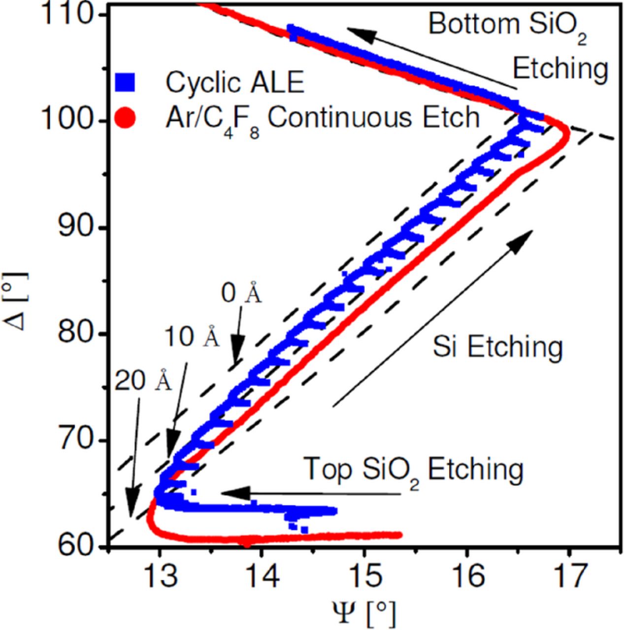
Figure 8. Real time ellipsometry trajectory showing key differences in surface processes between ALE and steady-state etching during continuous plasma etching of a SiO2-Si-SiO2 multi-layer stack.100 Each dashed line marks 10 Å of FC film.
Recently, Hudson et al.101 reported a similar highly selective SiO2 etch process based on repeated cycles of FC deposition and etch reaction activation using low energy ion bombardment.
While these FC deposition approaches are reminiscent of an approach called the "Bosch process" consisting of FC deposition during C4F8 passivation cycles followed by etching cycles using SF6, the Bosch process is primarily employed for deep reactive ion etching of silicon and the goal of the FC deposition is the achievement of sidewall passivation rather than as a source of etchant.102,103 Roozeboom et al.104 have proposed a method where this kind of process can be performed by horizontally moving the substrate back and forth during exposure to two chemically distinct gas discharges separated by inert gas curtains. This approach using ALD-based passivation may have potential as a basis of ALE processes.
TiO2
Park et al.105 studied ALE of TiO2 using 20 s adsorption of BCl3 followed by 60 eV Ar neutral beam bombardment, and measured 1.25 A/cycle. They report a critical BCl3 pressure of 0.16 mTorr and neutral beam dose of 1.49×10¹⁷ atoms/cm2 for these conditions, along with low surface roughness and no change in surface chemistry.
ZrO2
Lim et al.106 studied ALE of ZrO2 using adsorption of BCl3 followed by Ar neutral beam bombardment, and measured 1.07 A/cycle at the higher BCl3 pressures investigated (0.15 mTorr).
Issues and Needs
In this section we attempt to summarize several considerations of developments and opportunities that will be helpful for realization of ALE processes in manufacturing environments applicable to a broad set of reactant/materials systems. Additionally, we will briefly discuss features and challenges that will have to be overcome.
Scientific and technological basis of ALE
There has been a tremendous growth in knowledge in low temperature plasma materials processing/plasma etch science and technology since the first ALE studies. Examples are a) control of ionization, dissociation and uniformity across wafer,1,3,107,108 b) ion energy control,109 including using shaped waveforms,96 c) pulsed plasma science and technology,5 d) control of wafer charging and damage effects,110–112 e) plasma characterization and metrology,113,114 f) understanding of the control of plasma-polymer interactions, Line Edge Roughness, Line Width Roughness, CD and CD variation,115 advanced modeling and simulations of all of the above,116 and tremendous growth in advanced hardware engineering and capabilities.
Additionally, while true Atomic Layer Etching may be the ultimate goal for the most demanding applications, for many pattern transfer/dry etching applications dimensional control at the Angstrom level in combination with materials selectivity rather than true atomistic level control is sufficient. Indeed, the achievement of self-limited deposition and etching reactions by cyclic processing is deemed to be one of the key requirements on a practical ALE process, rather than achieving true atomistic resolution for each etching cycle.10
The above advances place atomic layer etching on a much stronger scientific and technological basis than the early efforts. In particular, the great advances in computational modeling of plasma and plasma/surface interactions have been important in designing and evaluating potential ALE approaches prior to experimental validation, e.g. as seen in the case of SiO2 ALE.9,95,99 Additionally, the somewhat relaxed expectations relative to true atomistic level control make the prospect of broad implementation more realistic.
The potential of precursor chemistry
Atomic layer etching also may be expected to have greater potential than conventional steady-state plasma etching to utilize the chemical nature of precursors and thus gain a new level of control over surface reactions. This ability is strongly reduced in continuous plasma processing, and has limited our possibilities of controlling surface reactions by choice of precursor molecular structure. Either exposure of a substrate to precursor gases without plasma or short plasma exposures offer the prospect of retaining a much larger proportion of the precursor molecular structure at the surface, and in this fashion impact etching reactions. The exposure parameters can be varied over a significant range, with steady-state behavior as a limit.
The surface composition of plasma-deposited FC films using C4F8 and CHF3 ALE processes for two thicknesses is shown in Fig. 9.100 The C1s spectra were determined after the deposition step during the 10th ALE cycle using X-ray photoelectron spectroscopy. Ultrathin FC films (∼ 3 Å) deposited using CHF3 exhibit a slightly higher F/C ratio composition than ultra-thin layers deposited using C4F8 (Fig. 9a). This is in contrast to continuous plasma etching, where the steady-state FC films formed from CHF3 typically show a significantly lower F/C ratio than FC films deposited using C4F8. This is due to both a high FC deposition rate for C4F8, and lack of hydrogen in the discharge which during ion bombardment of the film enhances F loss from the FC surface by HF formation for CHF3. For very thin ALE depositions the FC films reflect better the relative fluorine to carbon ratio of the feedgas which is higher for CHF3 than for C4F8. For thicker films of ≈15 Å (Fig. 9b), the F/C ratio of the film deposited by C4F8 is higher compared to the film deposited by CHF3. The surface chemistry differences between CHF3 and C4F8 seen for the thicker depositions are consistent with the findings of Standaert et al.24
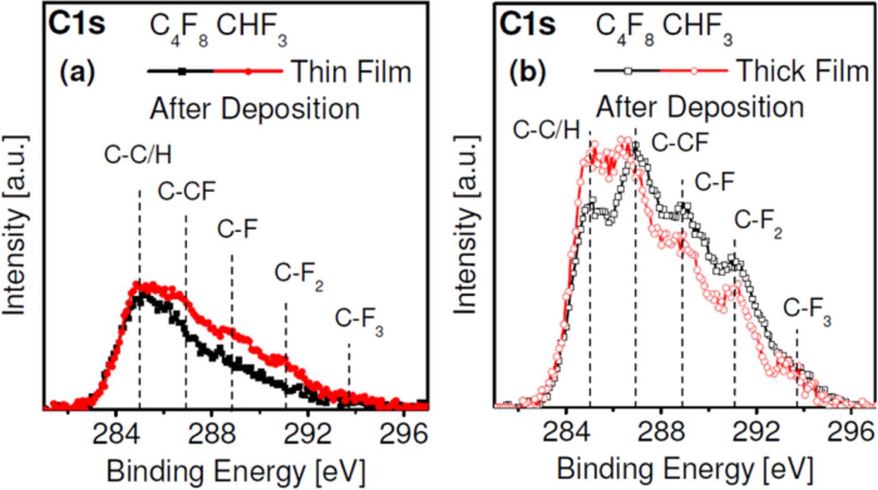
Figure 9. Enhanced potential of precursor choice relative to continuous plasma etching.100 The steady-state surface composition is not reached during a short deposition cycle (∼ 3 Å in (a)), whereas for the thicker (∼ 15 Å) film deposited in (b) the carbon 1s photoemission spectrum has become similar to that seen for FC films produced using continuous plasma processes.
Besides these helpful developments and features, there is a number of considerations and observations which demonstrate the difficulty of transiting ALE from research and development to manufacturing.
As discussed, although ALE shows some similarities to ALD with regard to physisorption/chemisorption requirements at the surface, the requirements with regard to "volatile product" removal are fundamentally different. Whereas for ALD films are grown in a conformal fashion, for ALE the "etch product" removal ideally should take place in a directional fashion, and requires energetic bombardment. The ALE window is located within a range of ion energies, and depends very sensitively on minute changes in surface chemistry (of the order of a monolayer). Because of this fundamental difference from ALD, ALE provides profound surface chemistry challenges and energetic species/surface interaction problems that are unique.
Reproducing sputter etching energy thresholds
To achieve self-limited etching in ALE, processing near the energy thresholds of physical sputtering is required. In Figs. 10 and 11 we have collected physical sputtering yield data by Ar ion bombardment with energies up to 400 eV for both Si and SiO2, respectively. SRIM simulation results and physical sputtering yields by Ar ion bombardment in the ALE work performed at University of Maryland99,100 are also shown. The surface sputtering simulation was conducted for ion bombardment normal to the surface using the software http://www.srim.org/. The simulation parameters are presented below.117

Figure 10. Review of literature data of physical sputter rates reported for Si versus the square-root of Ar ion energy up to energies of 400 eV95,118–132 along with SRIM simulation results. The threshold for physical sputtering of Si is ≈20 eV. The large scatter with regard to the threshold energy of physical sputtering for Si shows the difficulty of controlling experimental conditions.

The physical sputter yield of Si as reported in the literature95,118–132 when plotted versus the square root of the Ar+ ion energy shows a great deal of scatter around the energy threshold for physical sputtering (see Fig. 10). Similarly, the physical sputter yield data of SiO2 for Ar+ ion bombardment95,122,124,128,133–137 show significant scatter (see Fig. 11). While the data span many years, the scatter reflects the difficulty to reproduce these experimental conditions. For instance, differences in materials, e.g. single crystal silicon versus silicon thin films deposited on quartz microbalances, along with vacuum quality and other factors may explain some of the differences. Additionally, surface modifications during sputtering can change observed sputter yield, e.g. surface roughness, surface impurities, and so forth. Figures 10 and 11 illustrate that controlling etching behavior near the energy threshold for physical sputtering, i.e. close to the ALE window, is extremely challenging. On the other hand, physical sputtering will be most sensitive to small changes in residual impurities, and it is possible that for ALE the presence of chemical reactants at saturation coverage on a surface will overwhelm the factors leading to discrepancies and produce more stable and reproducible responses. Therefore, assuming that the energy of ions inducing physical sputtering can be precisely controlled, the ability to accurately control the flux of chemical reactants to the substrate is required.
Impact of surface reactions on plasma characteristics
The role of reactor surfaces (heterogeneous reactions) on continuous plasma etching process stability is well-known.3,138–141 One important difference between ALD systems and ALE systems is the overall energy content of ALE systems, in particular if plasma is used continuously and for all surface reaction steps. The result will be a highly dynamic environment where species transport between different surfaces can easily take place. For atomic layer etching, changes in the state of reactor surfaces and enhanced supply of reactants from "passive" surfaces (e.g., walls) by plasma-wall interactions could potentially lead to loss of control over the supply of chemical precursors to "active" surfaces. While plasma-enhanced surface passivation is desirable when considering throughput, the interaction of chemical reactants with "passive" surfaces will be enhanced for this situation. The formation of reactive radicals required to speed up adsorption processes at "active" surfaces will lead to greater interactions with "passive" surfaces which can become a supply of chemical reactants. Assuming a partial pressure of 10−4 chemical reactants for a plasma system operating at 10 mTorr pressure leads to the arrival of about 1 monolayer per s of chemical reactants during the process step whereas during the surface activation step no chemical reactants should be present to achieve a self-limited etch per cycle. Work needs to address what may be a proper balance between achieving ultra-clean processing/process control and rapid processing required for enhanced throughput.
This enhanced feedback from "passive" surfaces on plasma properties has been seen in the FC-based ALE of SiO2 and is demonstrated by Langmuir probe measurements during gas pulsing and shown in Fig. 12.100 Figure 12 displays the change in plasma properties, i.e. plasma potential Vp (Fig. 12a), electron density ne (Fig. 12b), and electron temperature Te (Fig. 12c), respectively, during one ALE cycle for two different conditions. These measurements show rapid changes of the electrical discharge characteristics during gas pulsing and additionally slow long-term changes in plasma electrical properties due to FC film buildup on walls. The increase seen for Vp and Te and the decrease of ne upon C4F8 precursor injection agrees with the impact on electrical properties for experiments using continuous precursor addition. For short pulses, the plasma properties return to values similar to those measured before the pulse within 20 s. A stronger and longer impact can be seen when increasing the C4F8 pulse length from 1.5 s to 5.0 s, and are consistent with the presence of residual precursor in the Ar plasma long after the initial pulse has been pumped out. Similar effects may be expected for other ALE chemistries, and point out the need for ALE process chamber designs and compensation techniques that will minimize these effects.

Figure 12. Evolution of plasma properties from cycle to cycle as measured using a Langmuir probe.100 The cycle-to-cycle changes increase with C4F8 pulse length due to more residual FC in the system. This is explained by more deposition of FC on the walls of the apparatus, contributing residual FC during Ar cycles when ideally FC is only present on the active surface of the substrate. The overall behavior is consistent with the impact of continuous precursor addition on plasma electrical properties.
Importance of photo-induced processes at low ion energies
Irradiation of surfaces by vacuum ultraviolet (VUV) light generated in plasmas can strongly affect surface reactions, and also give rise to synergistic effects. Donnelly's and Economou's groups46,142 reported on the importance of photo-assisted etching of silicon in chlorine- and bromine-containing plasmas for very low ion bombardment energies using nearly mono-energetic ion energy distributions. At this time the mechanistic origin of this observation is not well understood. The question of how important and generic photo-enhanced etching is for plasma-based ALE processes needs to be examined. This observation highlights the need to examine and understand the potential importance of simultaneous photon irradiation on ion-induced ALE processes in plasma environments in general.
Performance in 3-dimensional structures
Little is known at this time on the application of basic ALE procedures to advanced structures and applications. Plasma-enhanced surface passivation could potentially face limitations when considering substrates with pronounced surface topography. Radicals may have to undergo several surface collisions in order to reach the bottom of contact holes or trenches. The reduction in radical flux to surface elements at the bottom of features by surface recombination has been discussed extensively,36,39,107,143 and depends strongly on the value of the recombination coefficient r. This potentially could lead to situations where one location and material may exhibit self-limited adsorption at a monolayer, whereas another material may show multi-layer adsorption. Additionally, the redeposition of etch product on the feature sidewalls has to be considered.9 These phenomena could complicate the application of certain ALE processes to high aspect ratio structures.
Conclusions
As critical dimensions of semiconductor devices approach the sub-10 nm scale, the industrial need for an etching method capable of near-atomic resolution has led to a large increase in activity on novel directional etching methods based on a sequence of individual, self-limited surface reaction steps. The ability to achieve controlled, self-limited removal of various films at the Angstrom-level has been demonstrated for a range of reactant/materials systems, although specialized equipment with low throughput has often been used. Since for many situations true atomistic layer removal is not yet required and self-limited processing at the Angstrom scale appears sufficient, recent efforts have focused on increasing the speed with which self-limited surface reaction steps can be realized using plasma etching systems with enhanced temporal control of power, substrate biasing and gas delivery/pumping. A key challenge will be the insertion of ALE approaches into manufacturing. Since the overall energy content of ALE systems is expected to be significantly higher than for typical ALD systems, in particular if plasma is used during all reaction steps, this will produce a highly dynamic environment where species transport between different surfaces can easily take place. Maintaining controlled etching behavior for such systems within the ALE window near the energy threshold for physical sputtering is extremely challenging and will require stringent control of system cleanliness and the state of "passive" surfaces. These efforts are expected to benefit from advances in ALE chemistries and approaches. Computational modeling has been important in designing and evaluating potential ALE approaches and is expected to play a crucial role in the future for pin-pointing/appraising opportunities.
Acknowledgments
The authors gratefully acknowledge the financial support of this work by the National Science Foundation (CBET-1134273), US Department of Energy (DE-SC0001939) and Lam Research Corporation. The authors also thank E. Vogli, M. Vollmer, N. Fox-Lyon, E. Bartis, A. Knoll, P. Luan, D. Kaplan, Th. Pitzel and M. Kawakami for contributions during phases of this project. We also thank R. L. Bruce, S. Engelmann, and E. A. Joseph of IBM Research, V. Godyak, and E. Hudson, S. Lai, M. Danek, and A. Dulkin of Lam Research Corporation for helpful discussions and collaborations on ALE.