
Abstract
In this paper, we will review recent developments in scintillators, with a focus on scintillating materials for application in Computed Tomography (CT) and Positron Emission Tomography (PET). Main emphasis in the paper is on the translation of device requirements into material properties that need to be obtained. We will do this in particular to improve light yield (number of visible photons per keV of excitation energy), emission spectrum and decay time.
Export citation and abstract BibTeX RIS
Description Computed Tomography (CT) and Positron Emission Tomography (PET) medical imaging equipment
CT
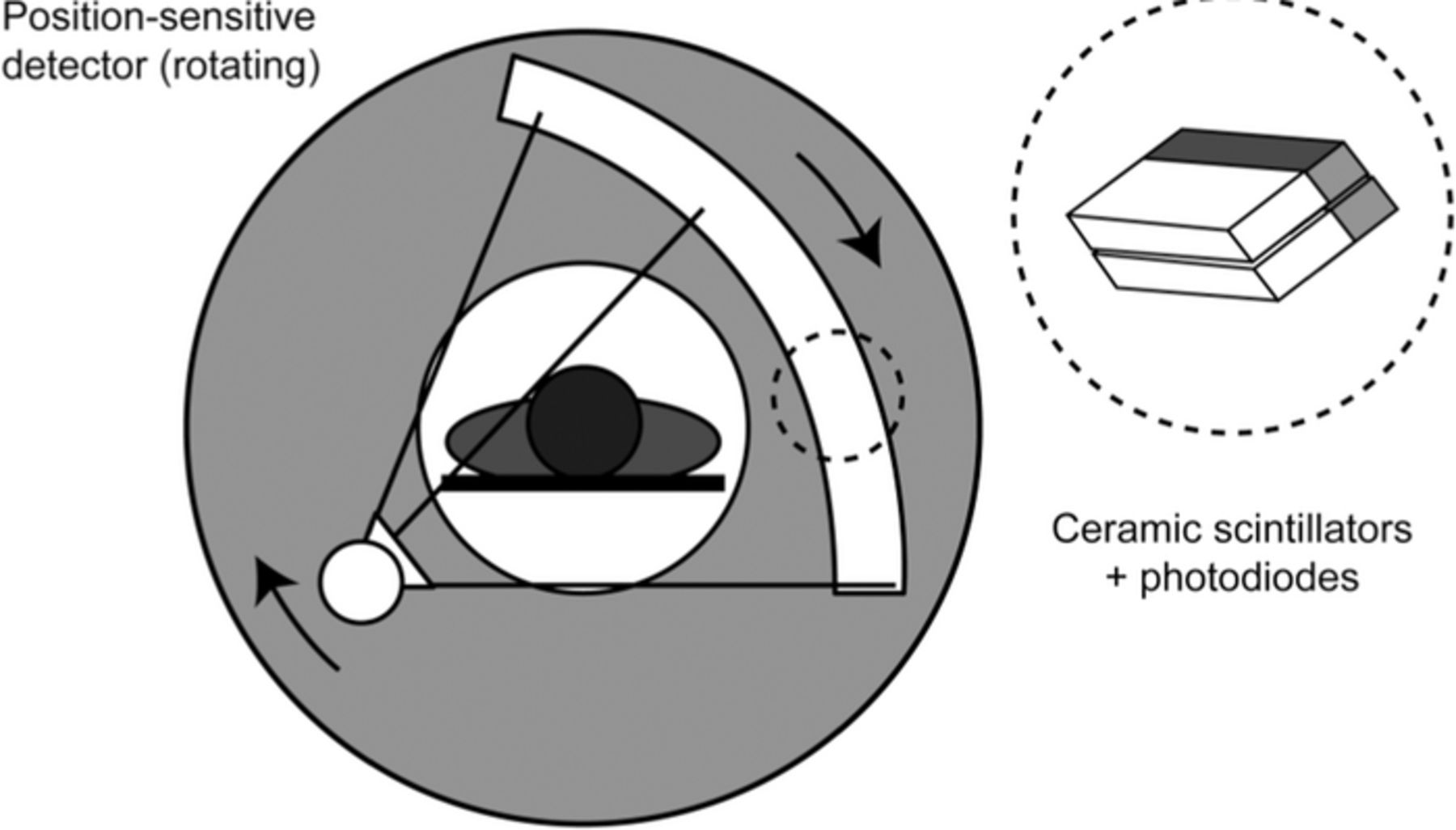
In a CT procedure, the patient is exposed to X-ray radiation that traverses through the body. The transmitted radiation hits a scintillator array that transforms the radiation into visible light. The visible light is detected by a photodiode array. A scan of the complete body can be obtained by rotating the X-ray source and the X-ray detectors (the positions of which are fixed relatively to each other) and moving the patient in a direction perpendicular to the rotation, see Figure 1. In modern CT machines, the rotation frequency is a few Hz. The images obtained using this procedure are anatomic images of the body, they contain 3D information about density differences in the body.
PET
In a PET procedure, the patient is injected with a radioactive tracer that emits positrons. The positrons emitted annihilate with electrons in the body of the patient which subsequently annihilate each other. As a result two photons are emitted, each with the energy of the rest mass of an electron (511 keV), under an angle of ∼180°. Only in this way, both momentum and energy can be conserved in this process. These two high energy photons are detected in coincidence using a ring of scintillators around the patient. This defines the so-called line of response (LOR). Apart from the photon energies and the angle of ∼180o, no other parameters are fixed, which means that the LOR can have any orientation. At the place where the tracer is enriched all LOR corresponding to this area therefore cross. In cancerous tissue, a lot of energy is being consumed: a radioactive marked sugar will enrich this tissue. PET images are functional images as they are related to processes taking place in the body.
A relatively new development is time-of-flight (TOF) PET. In TOF-PET, in addition to the LOR, also the difference in arrival time of the two high energy photons is measured (see Figure 2). This gives an increase in the spatial resolution (down to ca. 2 mm).
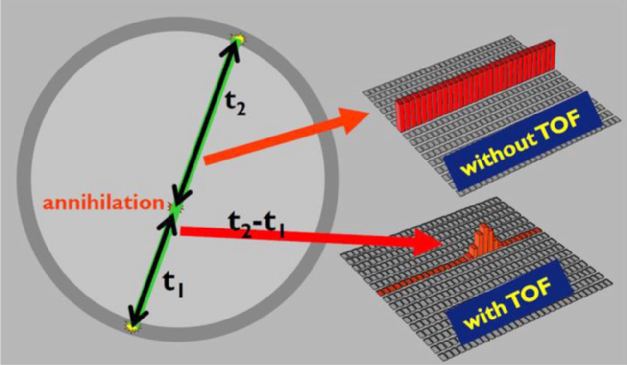
Figure 2. PET configuration. The patient is located in the scintillator ring. Two γ-quanta are formed on the annihilation of an electron and a positron. Using Time-of-Flight (ToF) the area on the LOR used in image reconstruction can be restricted, leading to a better signal-to-noise ratio in the reconstructed image.1,2
Maximum Light Yield
To improve basic scintillation characteristics (light output and decay time) the process of energy conversion in the scintillator should be studied in detail. The scintillation process in inorganic scintillators can be divided into the following three steps:3,4
- (1)The ionization event creates an inner shell hole and an energetic primary electron, followed by radiative decay (secondary X-rays), nonradiative decay (Auger processes and secondary electrons), and inelastic electron–electron scattering in the time domain of ∼10−15–10−13 s; the electron cascade, that is, the production of electron-hole pairs.
- (2)Thermalization, whereby the electrons and holes thermalize to the bottom of the conduction band and the top of the valence band, respectively.
- (3)Radiative emission either via the recombination of electron-hole pairs at lattice sites or through energy transfer to luminescence centers, followed by emission
The scintillator light yield LY is given by the total number of emitted photons Nph. The excitation of the luminescence centers occurs predominantly by the thermalized electrons and holes. The number of the thermalized e-h pairs is determined by the average energy Eehneeded for the creation of a single e-h pair. The value Eeh depends on kind of the crystal and the band-gap width Eg: Eeh = β.Eg, where β is a numerical coefficient, which reflects the mean energy losses of electrons and holes during their thermalization.3,4 Consequently, the number of the thermalized e-h pairs Neh = E/(β.Eg), where E is the the absorbed energy (e.g. from γ- or X-ray radiation). Now the light yield can be written as (taking 1000 eV as the quanta of energy absorbed, other energies similarly):
![Equation ([1])](https://content.cld.iop.org/journals/2162-8777/5/1/R3121/revision1/jss_5_1_R3121eqn1.jpg)
In which Eg is in eV, ηact the quantum efficiency of the activator, ηt the transfer efficiency of energy from host lattice states to activator states and ηesc the probability that low energy photons generated in the scintillator process leave the material.
The quantum efficiency ηact can be measured by direct photoexcitation of the activator. For many activators (Tl+, Ce3+, Eu2+, etc.) ηact is close to unity in the absence of a quenching. It is much more difficult to determine the transfer efficiency ηt. The second stage of the scintillation process involves transport and simultaneous or subsequent capture of a hole and an electron by an activator. The holes and electrons migrating through the crystal can also be captured by traps and/or take part in non-radiative recombination resulting in a low scintillation yield.
If we take ηact = ηt = ηesc = 1, we obtain the maximum light yield
![Equation ([2])](https://content.cld.iop.org/journals/2162-8777/5/1/R3121/revision1/jss_5_1_R3121eqn2.jpg)
Equation 2 reflects the so-called fundamental limit of scintillators, which is larger in materials, either intrinsic or activated, with small β and Eg.
In the following part, we will deal with the just derived expression and use a factor of 2.5 for β. This implies that β is host-lattice independent in this treatment, see also.4,5 In the majority of papers dealing with LY in scintillators, this value (2.5) for β is being used. This treatment is in clear contradiction with an earlier treatment by Robbins,6 in which β is strongly host lattice dependent. There is ample experimental evidence, however, that the description of the LY with a host-lattice independent value for β describes reality rather well. Moreover, the development of high LY garnets is in agreement with the Bartram-Lempicki treatment, whereas the LY values reported in the literature (up to some 55–57 photons/keV7) are much higher than expected based on the Robbins treatment.
In the next chapter, we will discuss factors that influence the value of β, as a function of the nature of the bonding in the crystals. As a result, even higher light yields can be expected, especially in polar crystals.
Emission Spectrum and Temporal Emission Behavior
The emission spectrum of the scintillating materials should, of course, have a good overlap with the spectral sensitivity of the photodetectors.
In case of CT, nowadays these are usually Si-based photodiode arrays, for this reason, the emission spectrum of CT scintillators ideally is in the spectral range 400 – 900 nm.
In case of PET, the emission should be as fast as possible as two photons have to be detected in coincidence and essentially all photons have to be counted in a short time, preventing dead time, to obtain a high energy resolution. For this reason, activators are used with completely allowed optical transitions with emission at short wavelengths. This latter conclusion is based on the Einstein coefficients that relate the decay time to the emission wavelength: τem ∝ λem3. To be compatible with Si photomultipliers, the emission wavelengthhas to be larger than about 400 nm. As a result, Ce3+ is the only activator that can be used in a useful manner in PET machines with Si photomultipliers as photodetectors.
The emission rise time has to be short as well, to obtain a short coincidence resolving time that, in turn, determines the accuracy with which the difference in γ-photon arrival times can be determined in ToF-PET. Ideally, the emission intensity is highest immediately after the capture of the high energy photons by the scintillators (on a sub ns scale, as photons travel around 30 cm in 1 ns in vacuum). The emission can be delayed as a consequence of slow energy transfer from host lattice states to the activator ions, f.e. due to trapping. This can be self-trapping due to lattice relaxation, it can also be trapping on defect sites. Please note that when defects capturing electrons and holes are sufficiently deep, thermally stimulated luminescence can occur. In the actual scintillation process, they can lead to a clearly visible buildup on a very long time scale (up to seconds), due to trap filling.
Emission Spectrum in Relation to the Maximum Light Yield and the Decay Time
Emission spectrum and maximum light yield
We are now in a position to estimate the maximum light yield for scintillating materials, based on the emission spectra; next we will calculate the maximum light yield as a function of the decay time, for activators with allowed optical transitions. We do this treatment for the following activator ions: Ce3+, Pr3+, and Eu2+. The first two ions are sufficiently fast for PET applications, albeit that Pr3+ is only fast enough when the emission is of the 5d-4f and not of the 4f-4f type, with emission in the UV. Eu2+ is fast enough for CT, but too slow for PET.
Common to all these ions is that they also have an oxidation state that is one unit charge higher. It makes these ions prone to ionization of the excited state, this we will take into account explicitly in our treatment.
First we calculate the maximum light yield for ions showing photoionization as a function of their emission wavelength. Taking into account the Stokes Shift and the fact that the excited states should not ionize thermally, see Figure 3 below, we assume that the bandgap energy should be at least 0.5 eV higher in energy than the emission maximum. This accounts for the energy difference between the relaxed excited state of the activator ion and the conduction band and this is assumed to be independent of the specific activator ion.
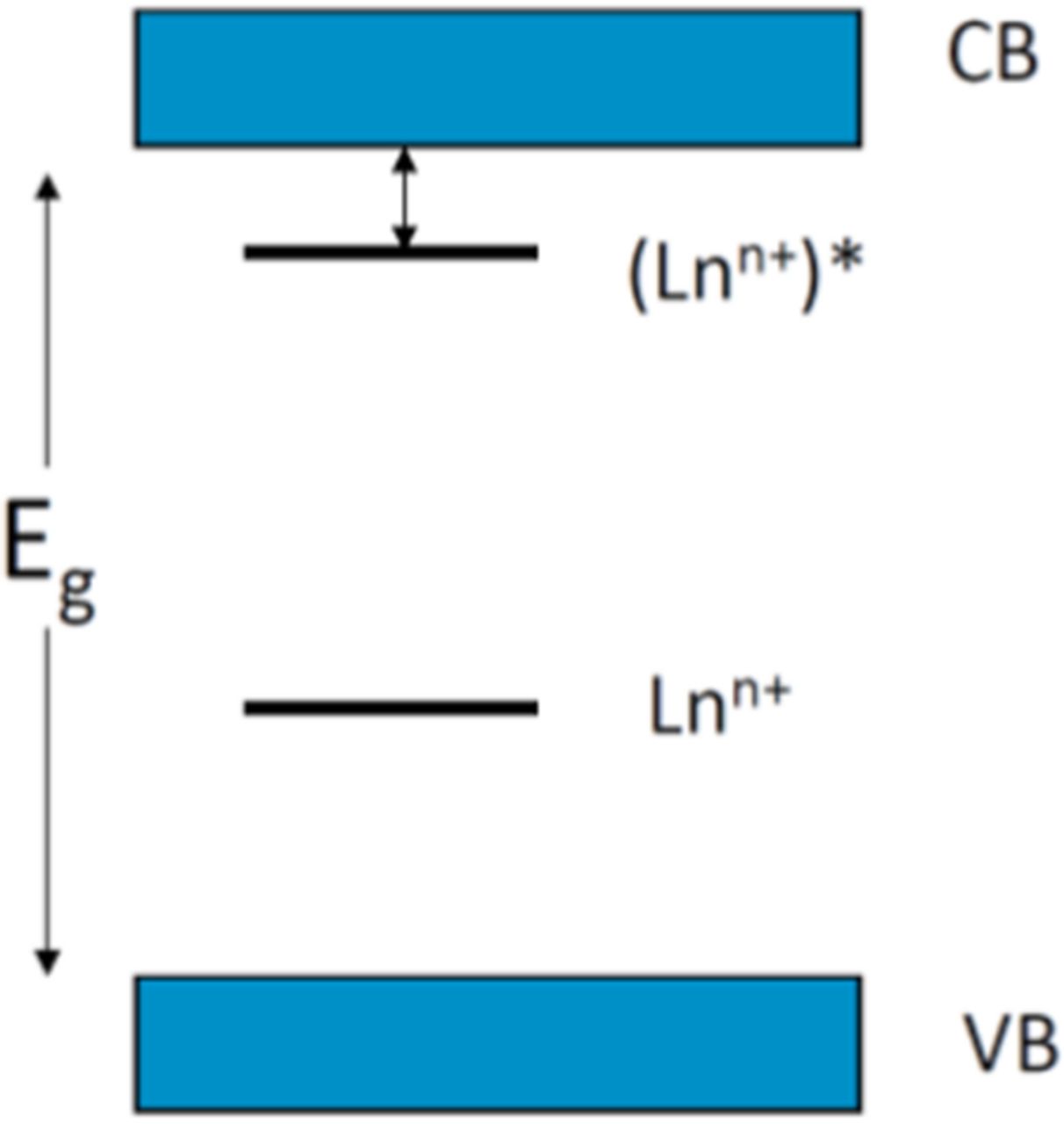
Figure 3. Thermal ionization of an excited activator by promoting an electron into the conduction band.
Next we do this for each of the activators, using the equation 2 for the LY and inserting the minimum energy values as lowest bandgap energy for each of the activators as derived from the lowest emission energies encountered in the literature (emission energy + 0.5 eV, see above). The combined results are given in Tables I–III and Figure 4.
Table I. Minimum values for the bandgap of scintillator hosts doped with the activators indicated for the lowest corresponding emission energies encountered.
| Activator | Emission observed | Minimum emission energy | Band gap minimum (eV) |
|---|---|---|---|
| Ce3+ | UV-Yellow | 2.5 eV | 3.0 |
| Pr3+(d-f) | UV | 4.0 eV | 4.5 |
| Eu2+ | Red | 2.0 eV | 2.5 |
Table III. Experimentally found highest light yield for host doped with Ce3+, Pr3+ and Eu2+.
| Activator | Host lattice | Light yield found (ph/keV) |
|---|---|---|
| Ce3+ | LuI3 | 100 – 1208 |
| Pr3+ | Lu3Al5O12 | 22 (own work, including f-f emission) |
| Eu2+ | CaI2 | 1109 |
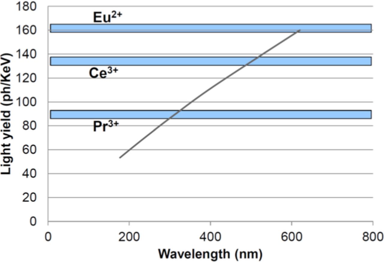
Figure 4. Maximum light yield (gray line) for scintillators doped with the activators indicated, with optically completely allowed transitions. The maximum values for each of the three activator ions are also given (β = 2.5).
In the Tables I–II shown below, we summarize the approximate smallest energies at which the emission maximum has been observed and subsequently we calculate the maximum light yields for four values of β (three values for materials with different bonding characters, see below, and for β = 2.5, a value frequently used). In Table III the highest light yields found experimentally are given.
Table II. Maximum theoretical light yields for scintillator hosts doped with the activators indicated for four different values of β (see further below).
| Maximum light yield (ph/keV) β | |||||
|---|---|---|---|---|---|
| Activator | Band gap minimum (eV) | 1.7 | 2.1 | 2.5 | 3.0 |
| Ce3+ | 3.0 | 196 | 159 | 133 | 111 |
| Pr3+ (d-f) | 4.5 | 131 | 106 | 88 | 74 |
| Eu2+ | 2.5 | 235 | 181 | 160 | 133 |
Comparing this to experimentally found values results in Table III.
From these Tables we observe that in none of the cases the maximum light has been reached. We also observe that the commercially used scintillators LuSi2O5:Ce (LSO) and Gd2O2S:Pr (GOS) are far off from the theoretical values. In case of GOS, the emission is of the 4f-4f type and located in the visible part of the spectrum. The bandgap is 4.4 eV so the estimated LY maximum still approximately holds, as the energy of the photons emitted is smaller than 3 eV. In the literature, a LY of 40 ph/keV is reported.1 Though used commercially, the light yield is at least a factor of 2 lower than the value that is theoretically possible. Interestingly, the LY of GOS, doped with Tb3+ is reported to be significantly higher, 60 ph/keV,1 which, however, still is significantly smaller than the theoretical limit, even for the largest value of β. Despite extensive research, no GOS scintillators have been developed with a LY that is near to the theoretical maximum. This very likely implies that the energy transfer from host-lattice states to activator states limits the LY.
In case of LSO, the LY is much smaller too, partly due to the relatively large bandgap (about 6.9 eV). Even if this is taken into account, the light yield could be considerably higher (some 60 ph/keV), rather than the value of 40 ph/keV found experimentally. The quantum efficiency of the emission on the activator is high, exceeding 90%, as judged from the emission decay time. So we again conclude that the energy transfer from host-lattice states to activator ion states limits the LY, this would open the possibility to still further improving the LY by material engineering.
Maximum light yield and decay time
In this section, we relate the maximum light yield and the decay time. We do this by using the following expression τem ∝ λem3 which relates the decay time to the wavelength, for optically allowed transitions.
As input, we use the experimentally found decay times in Lu3Al5O12:Ce and the corresponding maximum emission wavelengths. For Ce3+, the values are approximately 60 ns and 520 nm (19231 cm−1), for Pr3+ these are approximately 20 ns and 310 nm (32285 cm−1). Please note that the relative positions of the emission maxima are in accordance with earlier treatments by Blasse and a later refinement by Dorenbos, who came to the conclusion that the energetic positions of the 5d-4f excited states of Ce and Pr differ by about 12400 cm−1.10,5
This treatment now enables us to estimate the maximum LY as a function of the decay time. The maximum LY has been calculated already, we now calculate the corresponding decay times given the expression above. The results are given in Figs. 5 and 6.
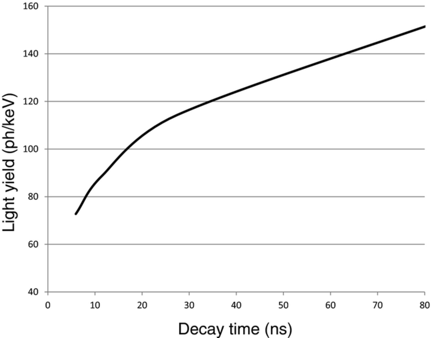
Figure 5. Maximum light yield for Ce3+ based scintillators as a function of the decay time.
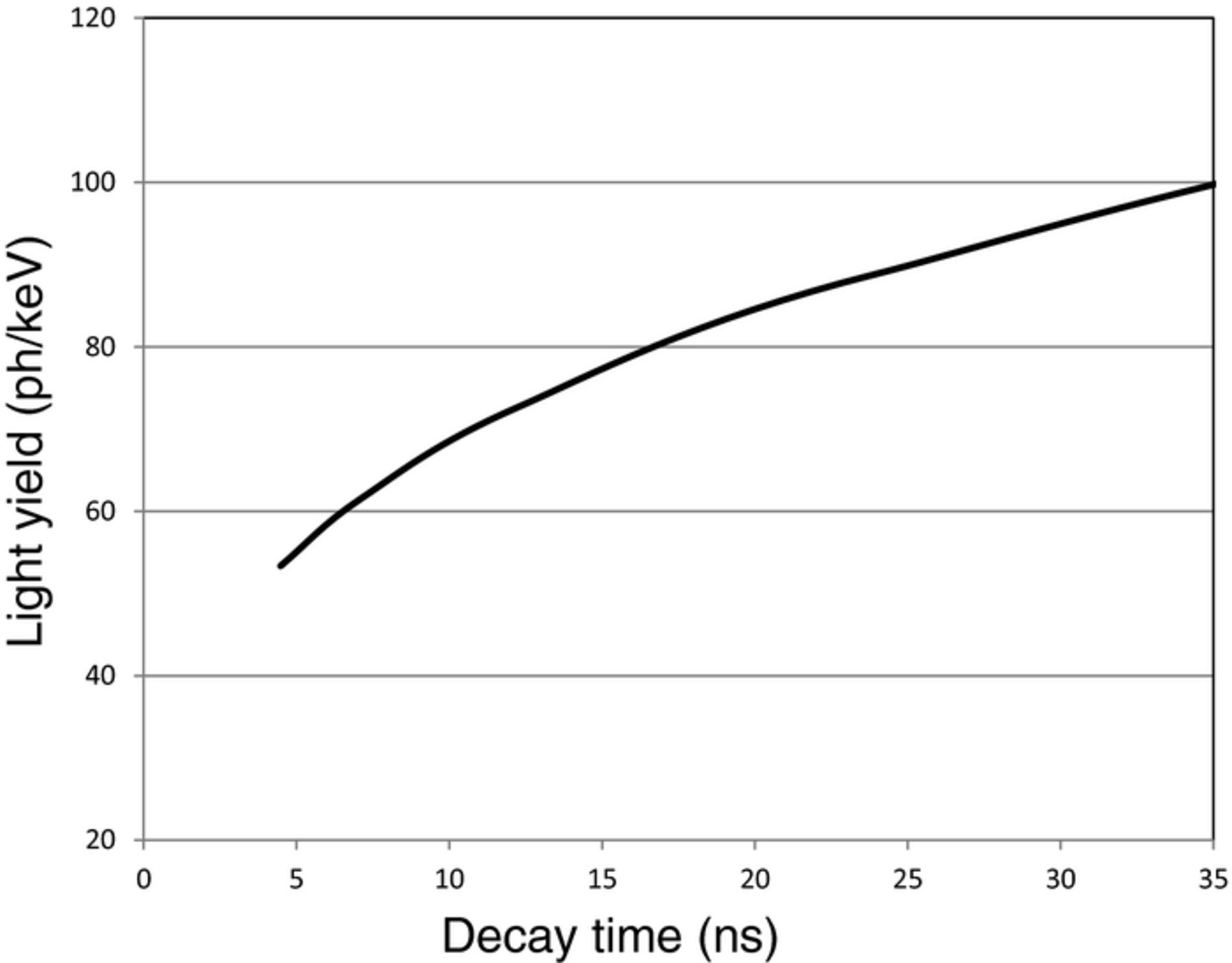
Figure 6. Maximum light yield for Pr3+ based scintillators as a function of the decay time.
Also here, we observe that LSO is far off from the maximum LY. The maximum light yield of garnets, doped with Ce3+, is about 65 ph/keV.7 This also is significantly less than can be expected based on the Ce3+ emission energy in this material. Also in this case the large bandgap plays a role (180 nm, 6.8 eV). Taking this into account, we conclude that garnets with light yield 65 ph/keV operate at physical limits.
From the graphs we also observe that, for the same decay time, the maximum light yield of Ce3+ based phosphors is higher than that of Pr3+ based phosphors. It implies that the transition matrix element Σf. |〈f|μ|i〉|² of Pr3+ is smaller than that of Ce3+. Indeed, when one calculates the Pr3+ decay time, using the Ce3+ decay time in the garnets and correcting for the difference between the Pr3+ and Ce3+ emission energies, one arrives at a decay time of 13 ns, whereas 20 ns is found experimentally.
This trend is observed throughout the lanthanide series, the allowed transitions on Eu2+ and Yb2+ are indeed much slower (μs-ms), very likely due to screening by the increasing number of f electrons.
Dependence of the light yield on β
In the previous section, we have given a general description for the maximum LY of scintillators as a function of the bandgap and as a function of the decay time. However, as we will discuss now, the value β itself depends slightly on the type of bonding in the crystal. Comparison of the experimental and theoretical data shows that for ionic (wide bandgap) crystals β ≈ 2 that is less than for typical semiconductors β ≈ 3.3 This difference can be understood from simple physical arguments. The value of β is larger for semiconductors because energy losses occur during thermalization of both electrons and holes while in ionic crystals the electron thermalization predominates, as these materials in general have relatively narrow valence bands.
The inorganic scintillators have been divided into three groups:
c) Crystals with covalent bond which have wide valence bands (ΔEv) and a small band gaps (Eg), the typical semiconductors belong to this group (β = 3.0)
c-p) Covalent-polar crystals with partial ionic bonding character, for which ΔEv < Eg(β = 2.1)
p) Polar crystals with ΔEv ≪ Eg and large Eg (β = 1.7)
The rule that the e-h pair creation energy Eeh is 3 times of the bandgap covers a large group of semiconductors: β = 3.0 in CdS, CdTe, GaP, PbO, and Ge.11,12 The crystals, which we refer to the group c-p have a lower value of the thermalization loss parameter: β = 2.2–2.3 in HgI2, AgBr, and AgCl;11,13 β = 2.1 in PbI2.12 For ionic crystals it is more difficult to determine the β value. It was found β = 1.40 in CsCl and β = 1.55 in KCl.14 In a recent experiment the energy of e-h pair creation Eeh of 10.8 ± 2.0 eV for NaI:Tl and 11.3 ± 2.1 eV CsI:Tl15 was obtained. This allows us to determinethe parameter β ≈ 1.7 for both of these materials. Using the above data, we have plotted the value 1/βEg vs. the bandgap of three types of crystals (Figure 7a). Figure 7b presents the experimental maximum LY of different compounds vs. the bandgap of the crystals. The curves in Figure 7b determine the light-yield fundamental limit, which decreases in the row covalent → covalent-polar → polar crystals.
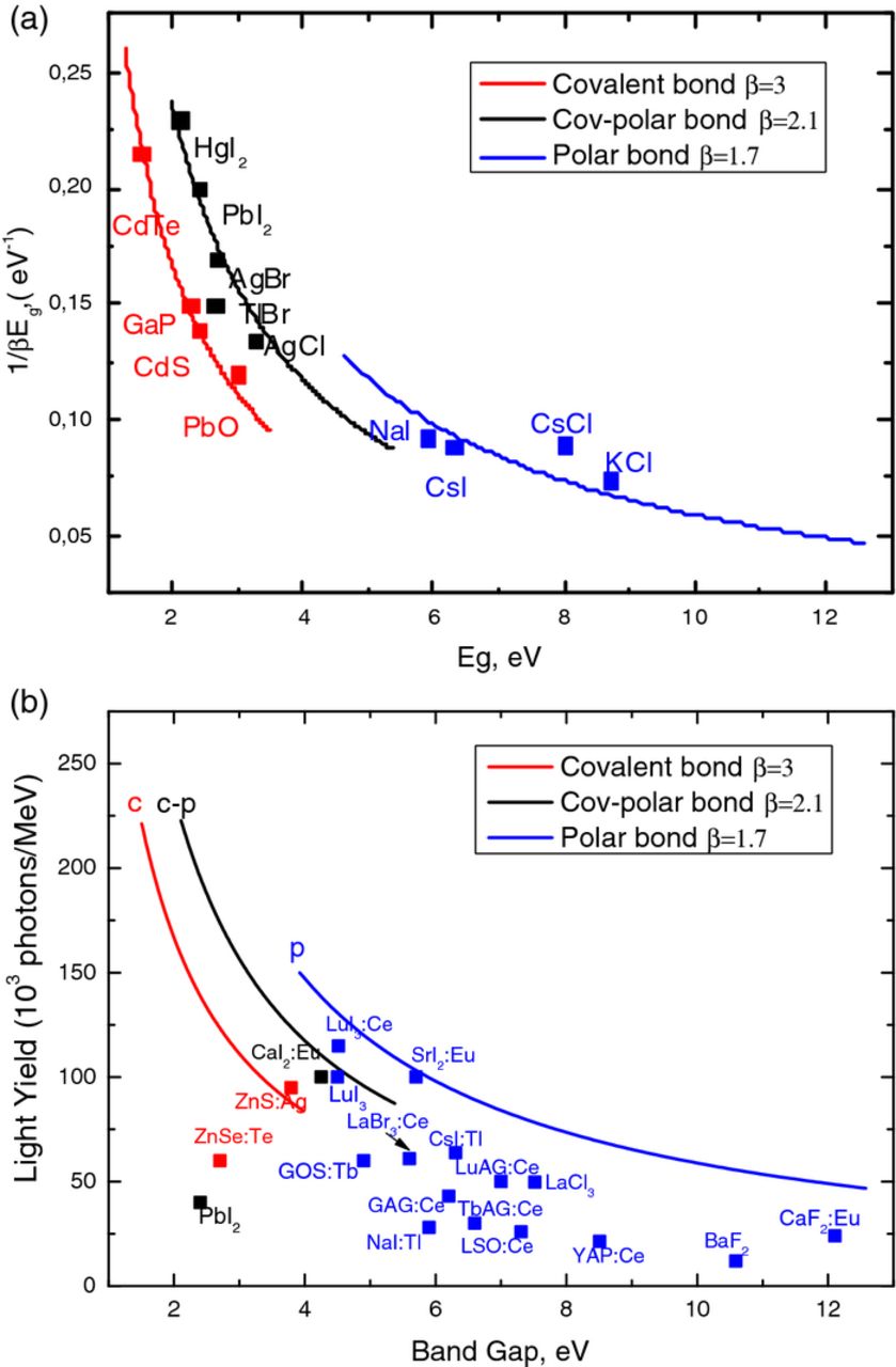
Figure 7. Figure 7a shows (1/(βEg) for a number of different materials, clearly showing different values for β for different kinds of chemical bonding. Figure 7b shows the resulting maximum light yields for three different values of β and the experimental results found for some well-known scintillators.
We observe that, in principle, much higher photon yields are predicted to be possible, especially for scintillators based on Eu2+. We also observe that indeed some materials have light yields that comply with a value for β of 1.7.
The value β = 2.5 is frequently taken in literature for all the crystals,4,5 see also above, which is simple but not general. The saving grace is in the fact that many scintillators in use are based on hosts which have a bonding character in between pure ionic and pure covalent bonding.
Consequences
Based on the different values for β, we now slightly reconsider our maximum light yield treatment. The results were already given in the Table II (see above). We observe that, based on this treatment, we may actually expect significantly higher light yields. This is only partially reflected in Figure 7b. Why is reality so much deviating from our predictions? There are a number of reasons:
- All activators treated in this paper have higher oxidation states, and in fact many efficient scintillators comprise activators that can have more than one oxidation state. Our treatment assumes that the excited state is located 0.5 eV below the conduction band. When this difference is smaller, thermal ionization can occur, reducing the light yield. This can be assessed experimentally by measuring the light yield at lower temperatures. When this difference is larger than 0.5 eV, the bandgap of the material has to increase, reducing the light yield, as otherwise the ground state is located in the VB. Then, reabsorption of the emission may occur by a charge transfer transition between the VB and the activator, also reducing the light yield.
- Incomplete transfer of electron-hole pairs to activator ions, in favor of transfer to centers for non-radiative recombination. In CsI, it was shown that at LNT, the light yield is significantly larger than 100 ph/keV;16 at lower temperatures diffusion to centers for non-radiative recombination may be less effective due to lattice relaxation.
- Localization of photoholes may occur when the coulomb interaction energy between two photoholes is larger than the width of the valence band, as the photohole states are pushed out of the valence band. Especially materials with a narrow valence band are prone to this effect. As a result, the photoholes are not mobile. Interaction with photoelectrons passing by may lead to Auger interactions, resulting in undesired energy losses. Similar considerations also hold for photoelectrons in the conduction band.
Conclusions
In this paper we have related the maximum light yield of scintillators to the emission color and to the decay time observed. This analysis was done using a value of 2.5 for β. In view of ample evidence that β depends on the type of chemical bonding, we have refined this treatment for the maximum light yield taking different values for β for materials showing chemical bonding with different nature. Significantly higher light yields can now be expected, especially for materials with polar bonds. Finally we discussed the impact of other factors that may limit the light yield.