
Abstract
To realize the potential of Gallium oxide (Ga2O3) Schottky rectifiers fabricated for high voltage and fast switching applications, various edge termination techniques to maximize the breakdown voltage (Vbr) are studied and examined via simulations using the FLOODS/FLOOPS TCAD simulator. The simulated Schottky rectifiers consist of a Si-doped (n = 1.0 × 10¹⁵ – 1.3 × 1017 cm−3) β-Ga2O3 epitaxial layer grown on Sn-doped (n = 4.8 × 1018 cm−3) Ga2O3 substrates. The optimization of field plate geometry for Schottky barrier diodes (SBD) was investigated using the device breakdown characteristics as the figure-of-merit. Various field plate dielectrics (SiO2, SiNx, Al2O3, and HfO2) were explored while the field plate structure was concurrently varied to obtain a normalized breakdown field (VNbr) of ∼3 for a step (graduated form) dielectric with Al2O3 as the dielectric. Edge termination via the formation of resistive areas at the anode contact periphery via ion (argon) implantation was also examined for the SBDs since other edge termination techniques are ineffective due to lack of p-type doping in Ga2O3. The configuration of the implanted region was investigated and a VNbr of over 5 was achieved for diodes with an unbounded resistive region and an implantation depth of 50–100 nm.
Export citation and abstract BibTeX RIS

This is an open access article distributed under the terms of the Creative Commons Attribution 4.0 License (CC BY, http://creativecommons.org/licenses/by/4.0/), which permits unrestricted reuse of the work in any medium, provided the original work is properly cited.
The need for new and improved high-performance power switching electronics has emerged due to the recent progress of power electronics, automotive electronics, grid-scale energy storage, industrial control, and military systems.1–8 Over the past few decades wide bandgap materials like GaN, SiC and Ga2O3 have been of interest to fulfill the requirements of electronic switching devices. Currently, state of the art devices have been fabricated from SiC and GaN, with GaN finding applications in fast-charging of home electronics,9 while SiC is commercialized for automotive charging applications. However, because of the larger bandgap of Ga2O3 (Eg = 4.5-5.0 eV), devices made on this material would have an advantage in terms of higher switching efficiency. The large bandgap translates to a high theoretical critical field strength (∼8 MV/cm), and a high Baliga's figure-of-merit (BFOM), about 4–7 times that of SiC and leads to low conduction losses at a lower cost (represented by Huang's chip manufacturing FOM or HCAFOM) in comparison to 4H-SiC diodes. Furthermore, recent advancements in the growth techniques of high-quality Ga2O3 substrates have made large, inexpensive substrates available using traditional growth techniques. In addition, high-quality epitaxial layers have also been grown using metalorganic-chemical vapor deposition (MOCVD), hydride vaper phase epitaxy (HVPE), and molecular beam epitaxy (MBE).10–16 High temperature operability is also possible due to the large bandgap; however, the low thermal conductivity is an issue with gallium oxide. Furthermore, additional limitations include the absence of p-type doping and the low electron mobility, which have sparked a lot of debate about the suitability of this material.
Using dopants like Si, Sn, and Ge, a wide range of electron densities (1015 to 1019 cm−3) has been demonstrated. Despite the various technological limitations of Ga2O3, the excellent breakdown characteristics make β-Ga2O3 Schottky barrier diodes ideal for low loss, high-voltage switching, and high-power applications. Over the past few decades, GaN and SiC devices have been developed to maximize the breakdown voltage (Vbr)17–25 by using edge termination techniques like field plate structures, highly resistive areas by ion implantation, guard rings, and mesas. The need for efficient edge termination arises because high electric fields are created near the contact edges as the reverse voltage is increased, which causes irreversible anode degradation. A lot of attention has been given to high current β-Ga2O3 Schottky rectifiers with focus on achieving high reverse breakdown characteristics and low on-state resistance (RON);26–29 however, edge termination has not been fully developed. The difficulty in implementing p-type doping has made it challenging to utilize edge termination techniques such as guard rings, or junction termination extensions, making field plate structures and ion-implanted regions near the contact edges the only available options.
A high Vbr of over 2300V27 has been reported for vertical large area field-plated β-Ga2O3 Schottky diodes fabricated on a 20 μm thick, very lightly doped (n = 2 × 1015 cm−3) epitaxial layer grown on a highly doped (n = 3.6 × 1018 cm−3) β-Ga2O3 substrate. Field-plated lateral β-Ga2O3 Schottky diodes30 have shown a higher breakdown voltage of over 3000 V while also demonstrating devices with very high DC power FOM of 370–500 MW/cm2. Progress on optimizing edge termination techniques for Ga2O3 rectifiers by Lin et al.,31 demonstrated the improvement in Vbr by using N++ ion-implanted guard rings. Theoretical studies have predicted nitrogen atoms to be deep acceptors,32 with the nitrogen impurities having acceptor transition levels of 1.3eV above the conduction band maximum.33 Various dielectric materials have been studied for field plated Ga2O3 diodes via simulation and initial reports34 suggest some good candidates in Al2O3 and HfO2 as the dielectric. Furthermore, edge termination via Ar ion implantation has also been studied for vertical Au/Ni/β-Ga2O3 Schottky barrier diodes35 where the area near the contact edges has been implanted to create highly resistive regions, which helps in diminishing field crowding near the contact edge. Similar to nitrogen ions as stated earlier, ion implantation creates defects in the materials that increases the deep acceptor trap concentration causing compensation in the intrinsic n-type doped material.
In this paper, a comprehensive analysis of various edge termination structures and techniques is performed via simulations to test the effects of dimensionality, dielectric materials, structural variations and trap concentrations on the breakdown voltage. Schottky rectifiers fabricated by Carey et al. are considered as the basic device structure36 with SiO2, SiNx, Al2O3, and HfO2 as the dielectrics, while the study by Gao et al.35 is used as reference and validation for the Ar ion-implanted edge termination analysis.
Methods
The FLOODS TCAD simulator self-consistently solves the partial differential equations governing the physics of our model. The Florida Object Oriented Device and Process simulator (FLOODS/FLOOPS) is a partial differential equation (PDE) solver, written as an extension to Tcl language for easy specification of PDEs and boundary conditions.37 The non-linear equations that are solved within are done so by the newton method and they are discretized in space using the finite-element method. In this work, we apply a two-dimensional model of the device structure to solve for the electric field distribution in the device. The model includes the common device equations like the Poisson's, continuity and current density equations. We solve for the electric field  by taking the gradient of the electrostatic potential obtained from the Poisson's equation.
In this work, the device design is optimized by studying the effect of dimensionality, structural variations and dielectric material on the reverse breakdown characteristics of vertical β-Ga2O3 Schottky barrier diodes. The model structure for the simulations given in Figure 1 is based on experimental study done on high current power rectifiers.27,36 The device was fabricated using a bulk n+ β-Ga2O3 (001) wafers grown by edge-define film-fed growth (EFG) and doped with Sn at 4.8 × 1018 cm−3, with a Si doped n-type epitaxial layer grown by hydride vaper phase epitaxy (HVPE) with doping concentration of 2.8 × 1016 cm−3. In our simulation, the effect of various epi-layer doping concentrations is also performed as seen in Figure 2 and we also observe that the bulk layer thickness does not affect the results, hence to reduce computing time we only simulate a 10 μm thick substrate.
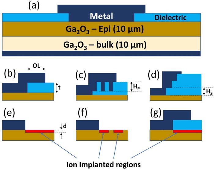
Figure 1. (a) Structure of the simulated Schottky diode based on literature. (b) Field-plated diode structure with 2 variables, i.e. Field plate overlap (OL) and dielectric thickness (t). (c) Field-plated diode pillar dielectric structure with a variable pillar height (HP). (d) Field-plated diode step dielectric structure with variable step height (HS). (e–g) Various structures simulated with Argon ion implanted resistive regions. The optimized solution between the ion implanted structures (e–g) according to the simulations would be (e) i.e. a highly resistive infinite implanted region.
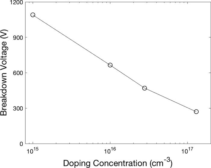
Figure 2. Breakdown voltage as a function of β-Ga2O3 Epi-layer doping concentration.
Figure 1 shows the field-plated structure used in the simulation, where the metal overlap (OL) and dielectric thickness (t) are varied to obtain the best dimensions for highest breakdown voltages. In addition to dimensionality, the suitability of the field plate dielectric material is also examined. The suitability depends on the relative permittivity, critical breakdown field strength and band offsets (Table I). This study also determines the breakdown characteristics of devices with SiNx, SiO2, Al2O3 or HfO2 as the field plate dielectric material. Figure 1 also shows various field plate structures which predict improvement in breakdown voltage based on a study done on diamond Schottky diodes.43 In this study, a pillar dielectric and graduated dielectric (step) geometry is examined for β-Ga2O3 Schottky diodes for different field plate dielectric materials, while varying the structural parameters as well.
Table I. Summary of the dielectric properties for simulated electric field.
| β-Ga2O3 | SiO2 | SiNx | Al2O3 | HfO2 | |
|---|---|---|---|---|---|
| Bandgap (eV) | 4.6 | 8.7 | 3.4 | 6.9 | 5.4 |
| ΔEc to Ga2O3 | - | 2.87 | - | 2.23 | 1.3 |
| ΔEv to Ga2O3 | - | 1.23 | - | 0.07 | −0.5 |
| Bulk dielectric Constant, ɛb | 10 | 3.9 | 7 | 9 | 25 |
| Thin Film Dielectric constant, ɛtf | - | 3.938 | 739,40 | 841,36 | 15.541,42 |
| Critical field Strength, | 5.235,26 | 10 | 6.740 | 8.736 | 5.343 |
| Ecr (MV/cm) |
Edge termination was simulated by forming a highly resistive region near the contact edges using ion implantation to spread the electric field in the device and prevent field crowding near the contact edge. Simulating the resistive region is achieved by incorporating a single mid-gap acceptor level (assumed to be gallium vacancy) with the implantation depth of 50 nm determined by TRIM simulation. The midgap state is incorporated using the incomplete ionization model we use exclusively for device simulations, given by Equation 1:
![Equation ([1])](https://content.cld.iop.org/journals/2162-8777/8/12/Q234/revision1/d0001.gif)
where ND+ is the ionized donor/acceptor trap concentration, Ntot is the total trap concentration, EF and ET are the electron quasi-Fermi levels and trap levels, respectively, and ∇E is the energy spread of the traps. The Full Width Half Max (FWHM) of the distribution is  . The trap concentrations are obtained by using the Stopping and Range/TRansport of Ions in Matter (SRIM/TRIM) code44 to get initial damage concentrations and using FLOOPS to simulate the Gallium vacancy diffusion during the low temperature anneal. The diffusion model for β-Ga2O3 is mentioned in earlier studies,47,48 which uses TRIM to generate input and then produces concentration profiles after annealing is done, by specifying the temperature and time of anneal. Gallium vacancies have been identified to behave as intrinsic deep acceptors in β-Ga2O3 and in some cases cause compensation to n-type β-Ga2O3 crystals.49 These parameters are obtained from initial work done by Gao et al.35 while validation to our results is also achieved for the two dose rates i.e. 5 × 1014 cm−2 and 1 × 1016 cm−2. Furthermore, simulations to see the effect of using both a field plate and an ion-implanted resistive region are conducted to inform the most efficient device structure. The simulations in this work are performed for respective structures using the same mesh and the same physical parameters in order to maintain homogeneity in the results.
Results and Discussion
The breakdown voltages for the un-terminated Schottky barrier diode as a function of the epi-layer doping concentration (Nd) are revealed in Figure 2; the results match the standard trend depicting an inverse relationship between the breakdown voltage and the doping concentration which has been observed for GaN and SiC diodes.17,22 A summary of the breakdown characteristics are shown in Table I with material parameters such as the dielectric constant, critical breakdown strength, bandgap and band offsets to β-Ga2O3. The breakdown voltage was calculated by the following method: FLOODS solves for the electric field being generated in the device at each element in the mesh at an applied reverse bias. The reverse bias is increased until a known critical field is achieved somewhere in the structure. The resultant 2-dimensional electric field distribution provides the location of breakdown, which is either in the epi-layer or the dielectric layer. Our results show good comparison between experimental and simulated values of un-terminated and terminated devices.27,30,36 Breakdown is sensitive to grid spacing, so the mesh was adjusted to reliably match the baseline results. The mesh was then used for all the other results.
A simple field plate termination structure as shown in Figure 1b with the metal overlap (OL) and dielectric thickness (t) is analyzed next. Figure 3a shows the normalized breakdown voltage (VNbr) as a function of OL for the different dielectrics but with a constant dielectric thickness of 0.36 μm. The normalized breakdown voltage is obtained by normalizing to the breakdown voltage of an un-terminated β-Ga2O3 Schottky diode. A peak in VNbr occurs for all the dielectrics near an overlap of 1 μm, and Vbr saturates to lower values for a field plate overlap greater than 4–5 μm. The saturation has also been observed for other studies24,45,46 and has been seen to occur when OL approaches the depletion width at breakdown (∼ 3–5 μm depending on Vbr for Nd = 2.8 × 1016 cm−3). This is due to the unnecessary extension of the field plate into the un-depleted semiconductor regions, assuming the lateral spread of the depletion region is comparable to the vertical spread of the depletion region. Additionally, the peak in VNbr at a field plate overlap of 1 μm is observed for structures with a dielectric thickness moderately lower than the optimal dielectric thickness (topt).46 topt has been found to be approximately 0.85 μm for the β-Ga2O3 SBD at the specific conditions. From the data in Figure 3a and for a dielectric thickness of 0.36 μm, the rise and fall of the breakdown voltage is mainly due to the respective reduction and increase of the electric field crowding at the field plate edge in the Gallium oxide.
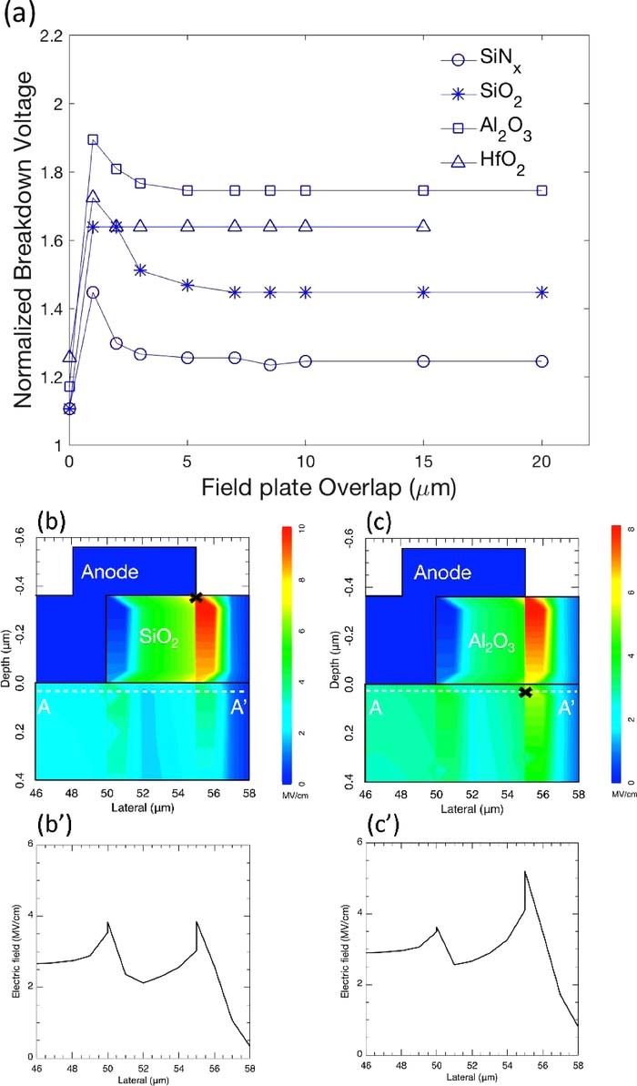
Figure 3. (a) Normalized breakdown voltage (VNbr normalized with respect to Vbr of an unterminated SBD) as a function of field plate overlap (OL) for the four dielectrics. (b) Electric field distribution in diodes with SiO2 as the dielectric, and (b') shows the electric field values along the A-A' line drawn in (b). (c) Electric field distribution in diodes with Al2O3 as the dielectric, and (c') shows electric field values along line A-A' drawn in (c). (b') and (c') show the comparison of electric field values in Ga2O3 epi-layer (near the interface), device is breaking down in epi-layer with Al2O3 as dielectric whereas the device is breaking down in the SiO2 layer with SiO2 as the dielectric (breakdown location marked by an "x").
The simulations also suggest that in the devices with a SiO2 or SiNx dielectric layer, breakdown occurs in the dielectric; whereas in the devices with a Al2O3 or HfO2 dielectric layer, breakdown occurs in the β-Ga2O3 epi-layer. This can be explained by the high dielectric constant (Table I) for both Al2O3 and HfO2 compared to SiO2 and SiNx, which means the β-Ga2O3 reaches its critical field before Al2O3 and HfO2 can reach their critical fields, whereas SiO2 and SiNx reach their critical field before β-Ga2O3 as the reverse bias voltage is increased. Breakdown locations for SiO2 and Al2O3 field plated β-Ga2O3 Schottky diode structures (OL = 5 μm) are shown in Figures 3b and 3c.
Similarly, Figure 4a shows the normalized breakdown voltage as a function of the dielectric thickness t, for the four different FP dielectrics considered in this study while the OL is kept constant at 10 μm. Intuitively, as the FP dielectric thickness is increased the breakdown voltage should also increase, as the electric field magnitude is inversely proportional to the dielectric thickness. However, as stated earlier the effects of the dielectric constant causes the early breakdown of larger thicknesses in low ɛ dielectrics. This effect can be seen in Figure 4a as we see discontinuity in the breakdown voltage as t is increased for SiO2 and HfO2. This discontinuity is explained by the breakdown location shifting from the dielectric to the β-Ga2O3 epi-layer or vice versa. Figures 4b and 4c help visualize this shift in the breakdown location for a device with SiO2 as the FP dielectric. We observed a shift in breakdown location from the dielectric layer to the β-Ga2O3 epi-layer at a thickness of 0.85 μm, while the figure compares two simulation results for a t of 0.7 and 1.0 μm.
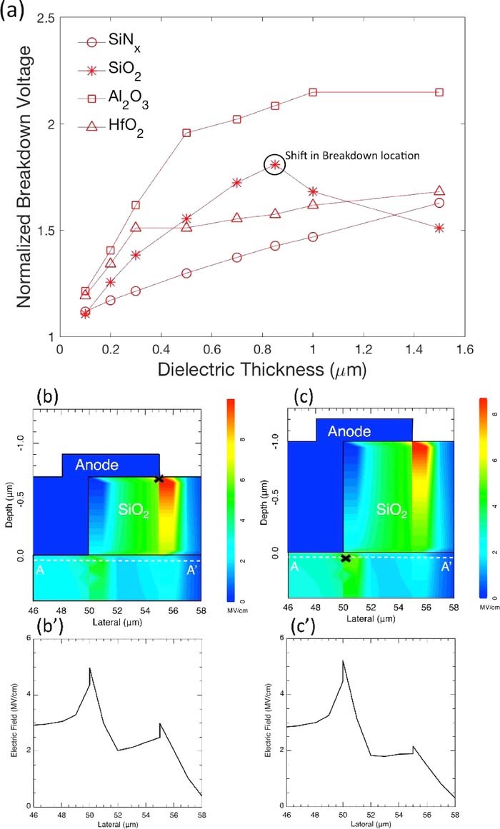
Figure 4. (a) Normalized breakdown voltage (VNbr normalized with respect to Vbr of an unterminated SBD) as a function of field plate dielectric thickness (t) for the four dielectrics. Electric field distribution for SiO2 dielectric field plate for t = 0.7 μm (b) and t = 1.0 μm (c). (b') Electric field values along A-A' drawn in (b). (c') Electric field values along A-A' drawn in (c). (b') and (c') show the comparison of electric field values in Ga2O3 epi-layer (near the interface), device breakdown location shifts from the SiO2 to the Ga2O3 epi-layer as t exceeds 0.85 μm (breakdown location marked by an "x").
A similar study was performed by Arbess et al.43 on a high-voltage diamond Schottky diode, where different FP structures like a pillar structure and a graduated dielectric form seen in Figure 1 are examined. This study along with previous studies on such diodes have shown that the maximum electric field is located just below the metal corners; and to mitigate this effect, corners are added to distribute the peaks. As shown in Figures 1c and 1d, this study focuses on one parameter for each structure i.e. the pillar height and the step height of the dielectric. As seen in Figure 5, for the graduated (step) dielectric form a VNbr of about 3 is observed for a step height of 1 μm for a Al2O3 dielectric. These results indicate that by using a graduated dielectric (or a tapered dielectric) FP a higher breakdown voltage can be achieved compared to a normal dielectric FP of the same total thickness.
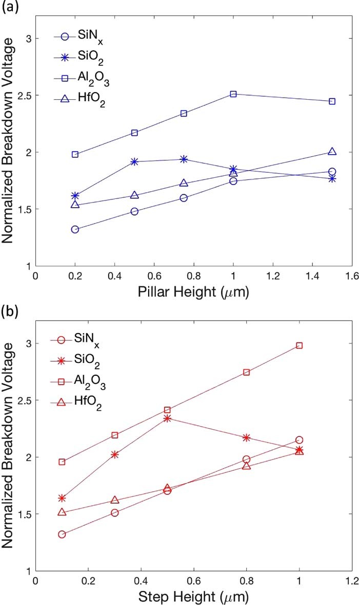
Figure 5. (a) Normalized breakdown voltage (normalized with respect to Vbr of an unterminated SBD) as a function of pillar height (HP) for the four dielectrics, with a VNbr of 2.5 achieved for device with Al2O3 as the dielectric (HP = 1.0 μm). (b) Normalized breakdown voltage as a function of step height (HS) for the four dielectrics, with a VNbr of over 3 achieved for device with Al2O3 as the dielectric (HS = 1.0 μm).
In order to study edge termination via ion implantation, the Schottky barrier diode is simulated with Ar ion implantation to form a highly resistive region at the periphery of the anode contact. GaO et al.34 performed the study for two different implant doses, while in this work the breakdown voltage is extracted as a function of the trap concentration after implantation and subsequent annealing. Figure 6 shows a plot of normalized breakdown voltage (VNbr) vs the trap concentration (NMG) of the midgap acceptor trap in the resistive region with a depth of 50 nm, at different epi-layer doping levels for a β-Ga2O3 Schottky barrier diode. A VNbr of over five is achieved for a diode with epi-layer doping as 2.8 × 1016 cm−3, while a VNbr of approximately two is achieved for a diode with epi-layer doping as 1.3 × 1017 cm−3. The curves level out for trap concentrations near and over 1019 cm−3 which is because the ideal plane parallel breakdown voltage determined for this device21,34 is reached at ∼1019 cm−3 NMG values. As observed in previous studies, the breakdown location shifts from the contact edge, to the edge of the resistive region 50 nm below the contact edge.
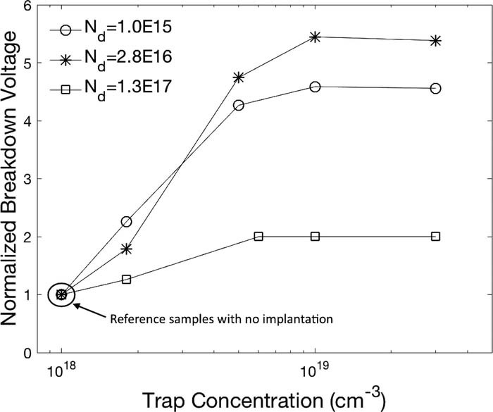
Figure 6. Normalized breakdown voltage as a function of midgap acceptor trap (gallium vacancy) concentration (NMG) for different epi-layer doping concentrations. Vbr has been normalized with respect to the breakdown voltage of non-terminated diodes, and the values for Vbr for Nd of 1 × 10¹⁵, 2.8 × 10¹⁶ and 1.3 × 1017 cm−3 are 1090, 470 and 270 V respectively for unterminated diodes. The ideal plane parallel breakdown voltage is reached for the device with NMG greater than 1019 cm−3.
Furthermore, we also simulated the structure in Figure 1f where multiple finite-implanted regions are formed and we achieve a VNbr < 2, hence suggesting devices with multiple implanted regions or finite implanted regions do not perform as well as devices with infinite implanted regions as seen in Figure 1e. This can be explained by the limited electric field spreading (or increased field crowding at corners) when multiple implanted regions are produced, compared to an infinite implanted region where a superior field spreading (or lower field crowding) is expected. For devices with both a field-plate and an ion implanted resistive region as seen in Figure 1f, the spreading of the electric field within the Ga2O3 epi-layer prevents any potential from being developed in the dielectric hence making the field plate ineffective. Finally, the breakdown voltage is simulated as a function of the depth (d) of the resistive region as seen in Figure 7a. Maximum value for Vbr is achieved for a depth of 75nm, and we see a gradual drop in Vbr as the depth of this region is increased, which could be attributed to increased resistance as the depth of the resistive region is increased. Further simulations reveal that due to the resistive area we observe bending of the electrostatic potential lines laterally across the device. The bending is observed just below the resistive area edge under the contact edge. As d is increased the electric field crowding near the resistive area edge increases, which results in a decline in Vbr.
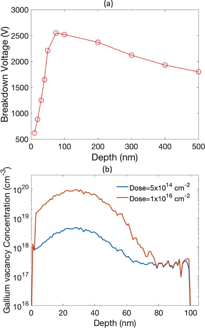
Figure 7. (a) Breakdown voltage as a function of the depth of the resistive (Argon ion implanted) region, for device with Nd = 2.8 × 1016 cm−3. (b) Concentration profile of gallium vacancies (midgap acceptor trap NMG) after the sample was implanted with Argon ions at 50 keV (TRIM) and annealed for 60 seconds at 400°C under N2 ambient (FLOOPS).
We also simulated the diffusion of the gallium vacancies after the argon implantation and developed a model to accurately predict the concentration of midgap acceptor traps (NMG). The concentrations achieved replicate the breakdown characteristics of diodes studied by Gao et al.34 where the 5 × 1014 cm−2 implant dose corresponds to a NMG value of 1.80 × 1018 cm−3 and a 1 × 1016 cm−2 implant dose corresponds to an NMG value of 3.0 × 1019 cm−3. The simulated concentration profiles of the midgap acceptor traps (gallium vacancies) are seen in Figure 7b for the two dose rates. This model would help in obtaining the gallium vacancy concentration after argon implantation at different implantation energies by using TRIM to simulate the initial damage concentrations, and then using the FLOOPS model to simulate the damage annealing and vacancy diffusion.
Conclusions
Edge termination for vertical β-Ga2O3 Schottky diodes was analyzed by simulating the electric field distribution in the diodes as the reverse bias is increased. The breakdown location of these Schottky diodes was located, and the field crowding near the contact edge was mitigated by utilizing edge termination techniques like field plates and highly-resistive implanted regions. Al2O3 is established as the superior field plate dielectric compared to SiO2, SiNx, and HfO2 by demonstrating VNbr of over 2 for standard field-plated diodes, while a VNbr of over 3 is achieved for the graduated form dielectric field-plated diode. Edge termination via argon implantation near the contact edges has resulted in even higher breakdown voltages for these diodes with a VNbr of ∼5 reported in this work. Furthermore, this technique is investigated in terms of the formation of deep acceptor states (gallium vacancies), diffusion of the gallium vacancies, depth of the resistive region, implantation energy and annealing parameters to develop a model to simulate this edge termination technique.
Acknowledgments
The project was sponsored by the Department of the Defense, Defense Threat Reduction Agency, HDTRA1-17-1-011, monitored by Jacob Calkins and also by NSF DMR 1856662 (Tania Paskova).
ORCID
Ribhu Sharma 0000-0001-5754-7873
S. J. Pearton 0000-0001-6498-1256